Article

Gamma-Irradiation-Induced Electrical Characteristic Variations in MoS2 Field-Effect Transistors with Buried Local Back-Gate Structure

1
Korea Atomic Energy Research Institute, 29 Geumgu-gil, Jeongeup 56212, Republic of Korea
2
Energy and Environment Materials Research Division, Korea Institute of Materials Science (KIMS), 797 Changwondaero, Sungsan-gu, Changwon 51508, Republic of Korea
*
Authors to whom correspondence should be addressed.
These two authors contributed equally to this work.
Nanomaterials 2024, 14(16), 1324; https://doi.org/10.3390/nano14161324
Submission received: 23 July 2024 / Revised: 3 August 2024 / Accepted: 5 August 2024 / Published: 7 August 2024
(This article belongs to the Section Nanoelectronics, Nanosensors and Devices)

Abstract

:
The impact of radiation on MoS2-based devices is an important factor in the utilization of two-dimensional semiconductor-based technology in radiation-sensitive environments. In this study, the effects of gamma irradiation on the electrical variations in MoS2 field-effect transistors with buried local back-gate structures were investigated, and their related effects on Al2O3 gate dielectrics and MoS2/Al2O3 interfaces were also analyzed. The transfer and output characteristics were analyzed before and after irradiation. The current levels decreased by 15.7% under an exposure of 3 kGy. Additionally, positive shifts in the threshold voltages of 0.50, 0.99, and 1.15 V were observed under irradiations of 1, 2, and 3 kGy, respectively, compared to the non-irradiated devices. This behavior is attributable to the comprehensive effects of hole accumulation in the Al2O3 dielectric interface near the MoS2 side and the formation of electron trapping sites at the interface, which increased the electron tunneling at the MoS2 channel/dielectric interface.

1. Introduction

In recent years, two-dimensional (2D) materials, including graphene, hexagonal boron nitride, and transition metal dichalcogenides (TMDs), have been proven to possess excellent properties, demonstrating their suitability for various applications, such as electronics, optoelectronics, sensors, energy storage, catalysis, and biology [1,2,3,4,5]. Among these 2D materials, MoS2 has been extensively studied because of its superior properties, including its ultrathin body, high carrier mobility, mitigation of short-channel effects, and tunable bandgap from 1.3 eV for bulk MoS2 to 1.8 eV for a monolayer [6,7,8,9,10,11,12,13,14]. These unique properties of MoS2 materials qualify them as promising candidates for channel materials in high-performance, downscaled, and low-power electronic devices and specialized radiation environments, such as those relevant to space, defense, and nuclear applications.
For radiation applications, ionizing radiation induced by the interaction between gamma photons and semiconductors can produce electron–hole pairs and diverse defects in the interaction materials, which can affect their structural and electrical properties. Radiation damage degrades the quality of the channel material, which in turn degrades the device performance. Conversely, atomic MoS2 with a layer thickness of approximately 0.65 nm offers excellent properties suitable for application in radiation-resistant devices because of its small volume that interacts with radiation [6]. Therefore, an in-depth understanding and analysis of radiation-tolerant technologies and the radiation response of TMD materials (e.g., MoS2) are critical steps in implementing radiation-related electronic devices for practical applications.
Although research on the effects of gamma radiation at the MoS2 transistor level is still in its initial stages with several technical challenges still to be addressed, experiments aimed at identifying the effects of gamma radiation on MoS2-based transistors and films have been conducted. For example, Isherwood et al. reported that high-dose gamma irradiation causes radiation damage, such as the radiolytic oxidation, doping, and etching of MoS2 flake films, which act as defect states within the MoS2 band gap, thereby degrading the device performance [15]. In addition, Vogl et al. reported the radiation tolerance of TMD-based devices using various irradiation sources, including gamma rays, protons, and electrons. The results indicated negligible variations in the current–voltage characteristics and photoluminescence intensity of mechanically exfoliated MoS2 devices that were subjected to gamma radiation [16]. Furthermore, Ozden et al. reported that the gamma radiation of few-layered MoS2 flakes created sulfur vacancies in the MoS2 structure, which were transformed into molybdenum oxide [17]. Moreover, Chen et al. performed gamma irradiation experiments on MoS2 transistors with solid polymer electrolyte gate dielectrics. After being subjected to gamma irradiation, the devices performed well; however, transfer curve changes and threshold voltage shifts were observed owing to the radiation-induced trapped electrons near the interface of the solid polymer electrolyte and MoS2 [18].
Although MoS2 materials offer promising prospects for downscaling integrated devices and circuit applications, the entire fabrication process is not fully compatible with the standard complementary metal–oxide–semiconductor (CMOS) process. Therefore, MoS2 synthesis on a high-quality large-area wafer scale is required. Chemical vapor deposition (CVD) has been identified as an effective method for producing high-quality TMD thin films on a wafer scale [19,20,21,22]. Most CVD synthesis methods involve providing transition metal sources, either in gas form or as predeposited metal or metal oxide precursor thin films on growth substrates [23,24,25,26]. The predeposition growth technique is a commonly used two-step process, in which transition metals (Mo and W) or transition metal oxides (MoO3 and WO3) are first predeposited on growth substrates and then sulfurized using a high-temperature thermal annealing process [27]. Although this simple two-step growth technique can provide large-area uniformity and layer-controllable growth, it is essential to transfer TMD thin films to target substrates to produce integrated electronic devices owing to the high-temperature CVD process [28]. In addition, the overall device performance is determined by certain crucial factors, including the contact resistance, dielectric scaling, and conformal gate controllability when designing device architectures [29,30]. Typically, MoS2 field-effect transistors (FETs) based on the conventional back-gate structure can achieve a nonuniform distribution for the gate electric field owing to the abnormal gate shape that occurs during the conventional lift-off process, which degrades the intrinsic electrical performance of 2D FETs. The implementation of a buried back-gate structure for uniform field induction improves the performance of the 2D MoS2-based FETs [31]. Furthermore, this gate geometry enables individual control of each device, which is essential for practical applications in CMOS-like logic devices. Therefore, understanding and analyzing the radiation responses of MoS2 devices are critical steps in the implementation of radiation-related electronic devices for practical applications. In contrast to MoS2 FETs with conventional top- or back-gate structures, the effects of gamma irradiation on the electrical performance of MoS2 FETs with a buried local back-gate structure have not been investigated (to the best of our knowledge).
In this study, we synthesized MoS2 film on the 2-inch wafer scale using two-step growth and fabricated MoS2 FETs with a buried local back-gate structure. The effects of gamma irradiation on the MoS2 FETs with a buried local back-gate structure were investigated. The electrical properties and gamma ray-induced changes in the MoS2 FETs before and after gamma irradiation were assessed. Furthermore, the possible interaction mechanism behind the electrical changes in the MoS2 and Al2O3 interface due to gamma irradiation was analyzed in detail.

2. Materials and Methods

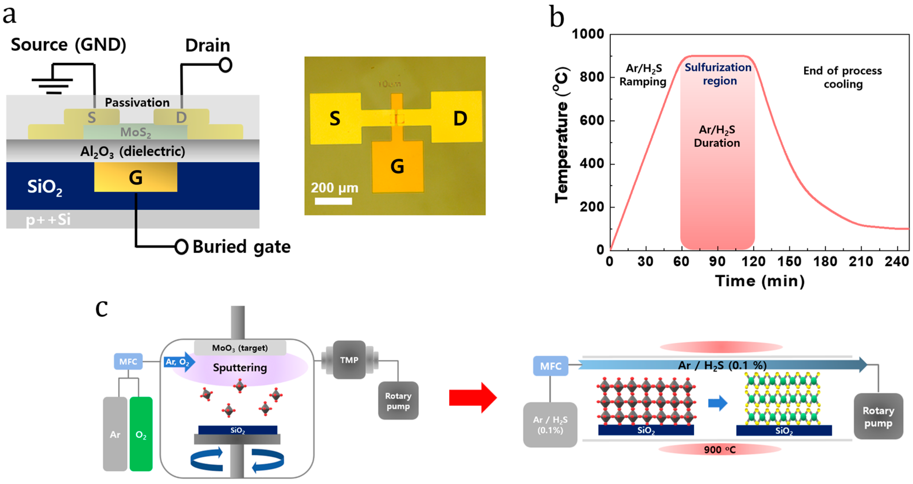
2.1. Device Fabrication

A photoresist (PR, AZ 5214) was coated onto a SiO2 (100 nm)/Si substrate using a spin coater. The coated substrate was baked at 110 °C on a hot plate for 50 s before being exposed to ultraviolet light (MDS-400s) for gate patterning. Subsequently, PR was removed using a developer (AZ 300 MIF) for approximately 40 s. A dehydration bake was then carried out on a hot plate at 90 °C for 5 min to remove moisture from the surface. The SiO2 layer of the gate-patterned area was etched via reactive-ion etching (RIE) with CF4 gas (30 sccm, 100 W, and 2 min). The depth of the etched SiO2 layer was approximately 50 nm. Subsequently, a Ti/Au (5/50 nm) layer was deposited using an electron beam evaporator. An Al2O3 layer with a thickness of 30 nm was deposited as the gate dielectric layer via plasma-enhanced atomic layer deposition. A 2D MoS2 thin film was coated with polymethyl methacrylate (PMMA, KAYAKU A5) to transfer the synthesized MoS2 films onto the Al2O3 dielectric. The coated MoS2 film was etched in a 5% hydrogen fluoride solution for approximately 30 s before being rinsed thrice with deionized water for 5 min each time. The PMMA/MoS2 film was then carefully transferred onto a gate dielectric layer. The wet-transferred MoS2 film was baked at 110 °C for 12 h on a hot plate. Next, the substrate with the MoS2 film was soaked in acetone and isopropyl alcohol, and then annealed at 200 °C in a high-vacuum environment of 10−6 Torr for 1 h to remove the PMMA. Au masking was performed for channel patterning to minimize the effect of PR residue on the MoS2 film. After depositing Au with a thickness of 20 nm, a channel was formed using photolithography. The region, excluding the channel, was selectively etched using a Au etchant. The active channels of the MoS2 film were formed via RIE, and the residual PR was removed using acetone, which was followed by annealing under the same conditions as described previously. Finally, Au with a thickness of 50 nm was deposited using an electron-beam evaporator for the source/drain process using the same pattern formation process. Finally, an Al2O3 layer with a thickness of 30 nm was deposited as a passivation layer via atomic layer deposition.

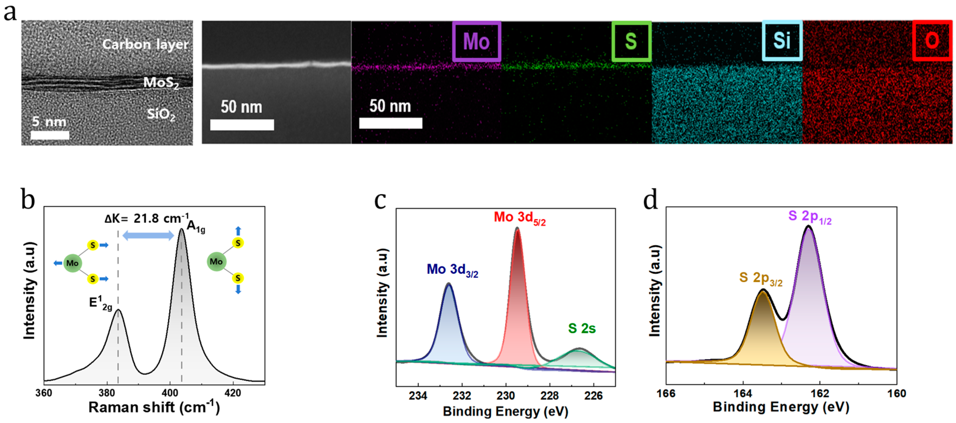
2.2. Characterization of MoS2 Film

Focused-ion beam transmission electron microscopy (FIB-TEM) was used to confirm the layered MoS2 film structure on the SiO2 (100 nm)/Si substrate. In addition, energy-dispersive X-ray spectroscopy (EDS) mapping was used to determine the elemental composition (i.e., Mo, S, Si, and O) of the samples. The synthesized MoS2 film was examined via Raman spectroscopy using a NANOBASE XperRAM-CS Raman spectrometer with 532 nm laser excitation. Finally, the components and chemical composition of the MoS2 film were comprehensively examined via X-ray photoelectron spectroscopy (XPS) using NEXSA equipment.

3. Results and Discussion

3.1. Synthesis of MoS2 on SiO2 Substrate

Figure 1a shows an illustration and an optical image of the 2D MoS2 buried local back-gate device. Figure 1b shows the temperature profile for the sulfurization of MoS2 via thermal CVD. The working pressure was maintained at 800 Torr using Ar/H2S (0.1%) gas at a flow rate of 200 sccm. The process of sulfurization involved gradually increasing the temperature from room temperature to 900 °C over 1 h and then maintaining it at 900 °C for 1 h. After completing this process, the temperature in the tube naturally decreased to room temperature. The two-step synthesis of the MoS2 film is shown in Figure 1c. First, the SiO2 substrate was radio-frequency-sputtered with approximately 3 nm of MoO3, and then it was subjected to thermal CVD sulfurization. Thus, the MoS2 films were successfully synthesized on SiO2 wafers.

3.2. Material Characteristics of the MoS2 Thin Films on the SiO2 Wafers

FIB-TEM was used to confirm the vertically layered structure of the MoS2 film on the SiO2 substrate. The elemental composition of the film was analyzed via EDS mapping, which revealed the presence of Mo, S, Si, and O. As shown in Figure 2a, the synthesized MoS2 film was multilayered, atomically flat, and smooth. The crystal structure of MoS2 consists of Mo and S, whereas the SiO2 substrate is composed of Si and O. As shown in Figure 2b, the Raman spectrum of the MoS2 film on the SiO2 substrate revealed two large peaks at 381.8 and 403.6 cm−1, corresponding to the in-plane vibration of Mo and S atoms (E12g) and out-of-plane (A1g) vibration of S atoms, respectively. The difference between the two MoS2 peaks was 21.8 cm−1, indicating that it was composed of four layers [32]. The MoS2 film components were further analyzed using XPS, as shown in Figure 2c,d. The XPS spectra of the Mo 3d and S 2s of the MoS2 film showed peaks at binding energies of 232.8 and 229.9 eV, corresponding to Mo 3d3/2 and Mo 3d5/2, respectively, whereas the peak at 227.1 eV represented S 2s. Two prominent peaks were observed in the XPS spectrum at 163.9 and 162.7 eV, corresponding to S 2p3/2 and S 2p1/2, respectively [33]. Additionally, the Mo:S composition ratio of MoS2 was calculated to be approximately 1:2.3, which is similar to the MoS2 stoichiometric ratio.

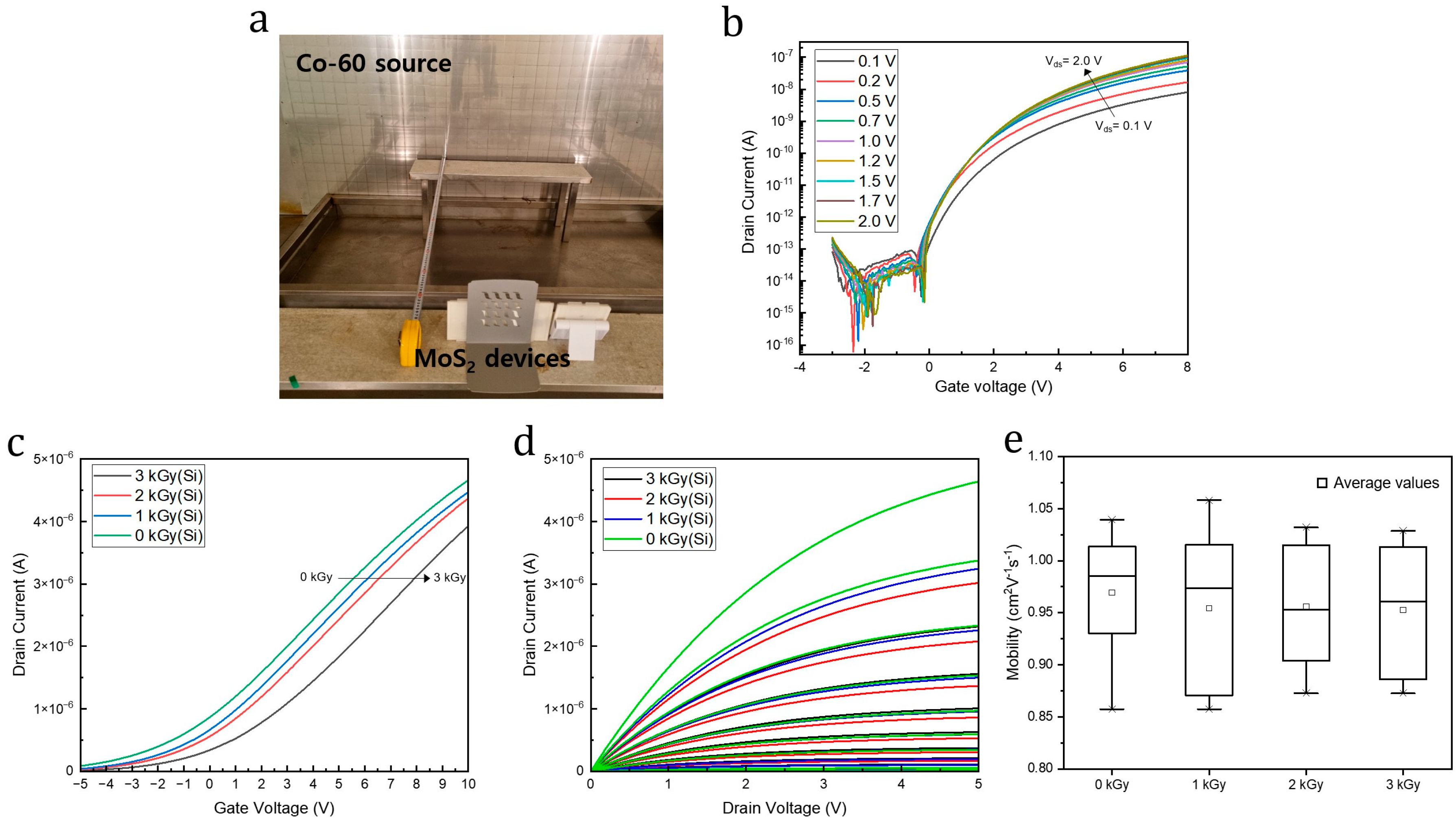
3.3. Gamma Irradiation Test Results for MoS2 Buried Local Back-Gate Transistors

Figure 3a shows the experimental setup for the gamma irradiation of the MoS2 samples. Irradiation experiments were performed in the irradiator facility at the Korea Atomic Energy Research Institute (KAERI). The Co-60 source, which comprises pencil-type modules, was kept in a pool of water when not in use and lifted out of the pool when needed for irradiation. The gamma rays from the Co-60 source had average energies of 1.17 and 1.33 MeV. The MoS2 samples were exposed to gamma radiation from the Co-60 source at a dose of approximately 1 kGy(Si)/h for various durations. Hereafter, the unit of kGy(Si) is denoted as kGy. All MoS2 samples were placed at a distance of 120 cm away from the Co-60 source according to the measured dose rates.
Current (I)–voltage (V) measurements were performed before and after radiation exposure to investigate the transient effects of gamma irradiation on the electrical properties of the MoS2 transistors. The transfer and output characteristics were measured at the total doses of 0 (non-irradiated), 1, 2, and 3 kGy. Figure 3b shows the transfer curves for the non-irradiated MoS2 transistors with gate voltages (Vg) ranging from −3 to 8 V at a fixed drain voltage (Vd) in the range of 0.1–2.0 V. The curves exhibit a typical n-type behavior, corresponding to the n-type electronic properties of the MoS2 semiconductor [8,34]. Moreover, the off-state current for Vg = −2 V was 10−14 to 10−15 A and the on-state current was approximately 10−8 A, indicating the efficient depletion of the device channel through the gate bias control. Thus, the on/off current ratio of the non-irradiated sample was 106–107, which is comparable to previously reported results and is sufficient for electronic applications such as switch devices [35].
Figure 3c shows the transfer curves for the MoS2 transistors before and after gamma irradiation for cumulative doses of 1, 2, and 3 kGy. The transfer characteristics were obtained by sweeping Vg from −5 to 10 V and setting Vd to 1 V. The current decreased as the gamma ray dose was increased. The current of the non-irradiated MoS2 transistors at 10 V decreased by approximately 15.7% after exposure to a gamma radiation dose of 3 kGy. The threshold voltages of −1.77, −1.27, −0.78, and −0.62 V were measured for the MoS2 transistors under exposures of 0, 1, 2, and 3 kGy, respectively. The positive threshold voltage shifts of 0.5, 0.99, and 1.15 V were observed for the MoS2 transistors under irradiations of 1, 2, and 3 kGy, respectively, compared to the non-irradiated device. Notably, 20 MoS2 FET devices were tested under gamma irradiation doses up to 3 kGy, with steps of 1 kGy, to verify data reliability. All MoS2 devices exhibited a similar trend of a positive shift in transfer characteristics. These positive shifts in the threshold voltages of the transfer curves are attributable to the comprehensive effects of hole accumulation in the Al2O3 dielectric interface near the MoS2 side and the formation of electron-trapping sites at the interface, which increased the electron tunneling at the MoS2 channel/dielectric interface. A more detailed explanation of the electrical changes caused by gamma irradiation is provided in Section 3.4.
Figure 3d shows the output curves for the MoS2 transistors before and after gamma irradiation at radiation doses of 1, 2, and 3 kGy, where Vd was swept from 0 to 5 V and Vg was varied from −5 to 3 V in steps of 1 V. As shown in the output characteristics, all MoS2 transistors exhibited drain-current saturation in the high-bias region and well-defined linear behavior in the low-bias region, indicating that the buried local back-gate bias completely controlled the channel carrier transport. Moreover, the drain current level decreased as the total gamma irradiation dose increased, indicating that gamma irradiation degraded both the channel quality and switching characteristics of the MoS2. As predicted, the degradation of the output characteristics followed a trend similar to that of the transfer characteristics. Although the degradation in the output current was observed after 1, 2, and 3 kGy of gamma irradiation, the channel conductance of all samples was efficiently modulated by the gate bias control, indicating that the switching characteristics between on and off states allowed for normal FET operations even after gamma irradiation.
To further investigate the effects of gamma rays on MoS2 channels, their field-effect mobilities ( μ F E ) were calculated using the following equation:
μ F E = d I d d V g L W C o x V d
where L represents channel length (20 μm), W represents channel width (50 μm), and Cox is the dielectric capacitance per unit area between the channel and the gate. As shown in Figure 3e, the average mobilities of 0.97, 0.95, 0.96, and 0.95 cm2V−1s−1 were observed for MoS2 transistors under gamma irradiation of 0, 1, 2, and 3 kGy, respectively. The result showed no significant differences between MoS2 devices before and after irradiation, indicating that the MoS2 layers could withstand gamma irradiation doses up to 3 kGy. Previous studies have reported that MoS2 layers can endure higher gamma radiation up to 10–130 kGy without any noticeable degradation in their properties [16,36,37].

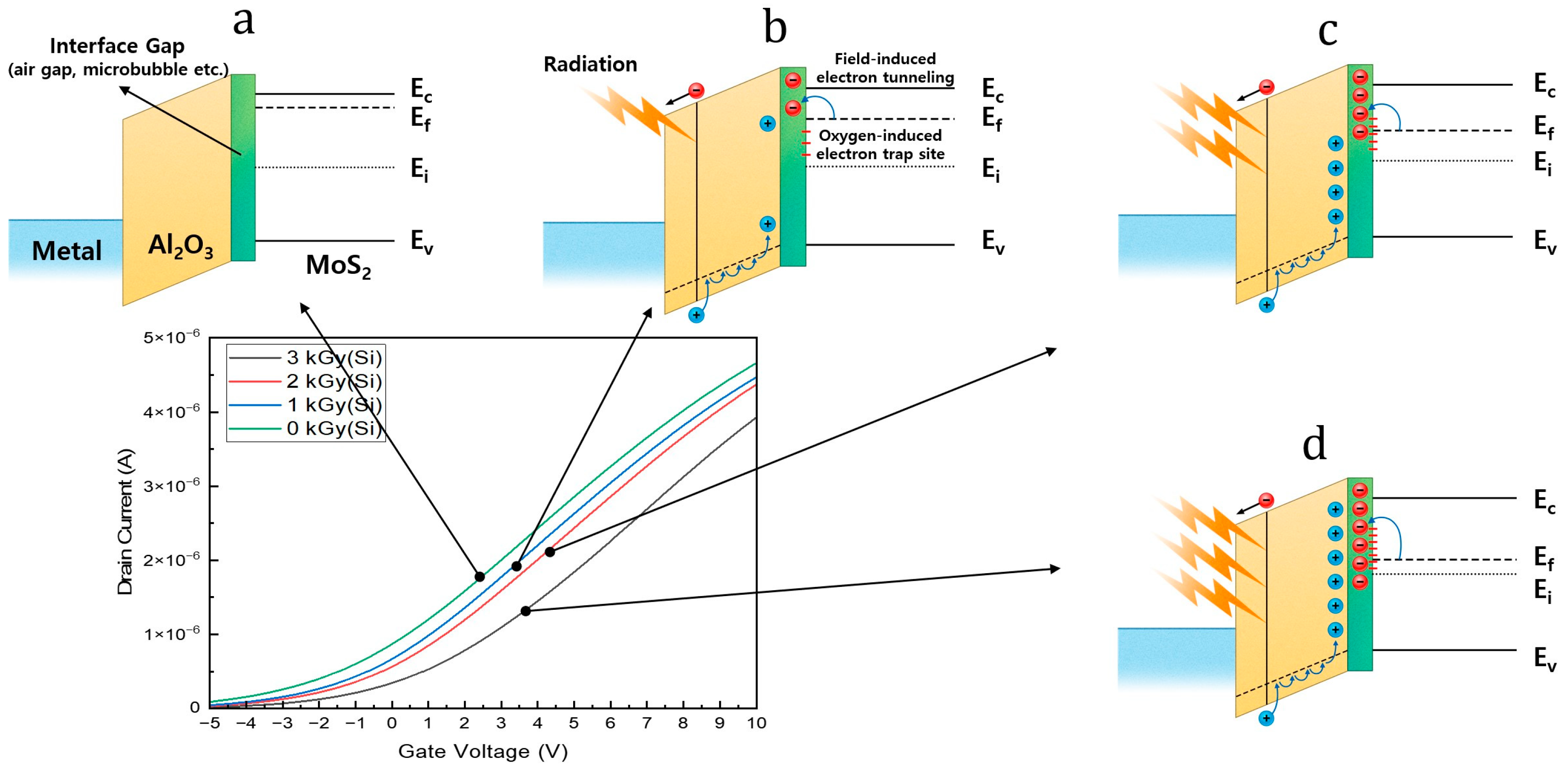
3.4. Mechanism of Electrical Characteristics Changing According to Gamma Irradiation Dose

Figure 4 shows the positive shift in the transfer curve as the gamma irradiation dose was increased from 0 to 3 kGy and the change in the band alignment of gate Al2O3–MoS2 under each condition. Similar to previously reported results [38], the transfer curve of the gamma-irradiated MoS2 transistor exhibited a positive shift. The mechanism for this phenomenon was analyzed. When a typical bulk metal–oxide–semiconductor (MOS) transistor is exposed to gamma rays, electrons and holes are generated in the oxide. Electrons escape the oxide at a high speed but holes cannot escape at a slow speed and are trapped at the interface, thereby degrading the transistor performance. Consequently, the off-current increases and shifts the transfer curve negatively owing to the positive field of the hole. When gamma rays are irradiated toward the MoS2 transistor, a positive shift, which is the opposite to that observed for the bulk semiconductor, occurs. This phenomenon has been reported as a carrier trapping/detrapping mechanism at the interface between 2D nanodevices and dielectrics [38,39,40,41,42], which can be explained in conjunction with the band diagram and Fermi-level shift. In an n-type MOS FET, the positive shift in the transfer curve signifies that more positive fields are needed to turn the transistor into the ON state. This result can be summarized in three situations: (1) the accumulation of a negative field source that interferes with the positive field in the gate oxide, (2) the intrinsic change in the Fermi level of the MoS2 channel owing to external factors, and (3) the trapping of electrons flowing in the channel at the interface. In the MoS2 transistor, all three of these mechanisms occur, and the primary causes are the air gap between the dielectric and MoS2 layers in the 2D nanodevice and the electron trap source that penetrates the grain boundary of the dielectric. When a gamma ray is incident on a MoS2 transistor, a hole is trapped in the surrounding dielectric interface, and electron tunneling occurs from the MoS2 channel to the surrounding air gap owing to the positive field of the hole. Consequently, the Fermi level of the MoS2 moves intrinsically [43]. Moreover, as the intensity of the gamma irradiation increases, the number of tunneled electrons increases. Therefore, as the magnitude of the gamma ray irradiation increases, the MoS2 channel changes intrinsically and the transfer curves undergo a positive shift. Additionally, gas molecules can penetrate the grain boundaries of the upper passivation layer [44], and a redox reaction occurs, causing MoS2 electrons to be used as a source. Furthermore, the by-product of the interfacial redox reaction is the OH group, which acts as a negative field source that prevents the positive field from accessing the gate. In addition, ozone created by the gamma rays in the atmosphere penetrates the grain boundaries and acts as an electron-trapping site [45]. The mechanisms described above produce a comprehensive effect, whereby a higher exposure to gamma rays results in more reactions and promotes a positive shift.

4. Conclusions

In this study, we successfully fabricated MoS2 FETs with a buried local back-gate structure and investigated the effects of gamma irradiation on the electrical performance of the devices. The transfer and output characteristics of the resulting devices were slightly degraded after gamma irradiation. Under a gamma irradiation dose of up to 3 kGy, the current level of the MoS2 transistors decreased by 15.7% compared to that of the non-irradiated devices. Moreover, the threshold voltage of the MoS2 transistors positively shifted by 0.50, 0.99, and 1.15 V after irradiation doses of 1, 2, and 3 kGy, respectively, compared to that of the non-irradiated devices. After analyzing the mechanisms involved, the positive shifts in the threshold voltages were attributed to the comprehensive effects of hole accumulation in the Al2O3 dielectric interface near the MoS2 side and the formation of electron trapping sites at the MoS2 channel/dielectric interface. Therefore, the results of this study provide a clearer understanding of the dominant factors that degrade the electrical properties of MoS2 transistors. The results also suggest directions for improving vulnerable regions and appropriate device configurations in high-radiation environments, such as those relevant to space, nuclear, and aerospace applications.

Author Contributions

S.J.K.: Conceptualization, Data Curation, Writing—Original Draft Preparation, Methodology. S.H.: Conceptualization, Data Curation, Writing—Original Draft Preparation, Methodology. J.-D.K.: Formal Analysis, Investigation. J.Y.: Formal Analysis, Investigation. J.M.P.: Formal Analysis, Validation. Y.L.: Formal Analysis, Validation. Y.K.: Writing—Reviewing and Editing, Supervision. C.G.K.: Writing—Reviewing and Editing, Supervision. All authors have read and agreed to the published version of the manuscript.

Funding

This work was supported by the Korea Atomic Energy Research Institute (KAERI) Institutional Program (project numbers 523510-24 and 523160-24) and Grant RS-2022-00144108 funded by the Ministry of Trade, Industry, and Energy of the Korean Government. This study was also supported by the Fundamental Research Program (PNK9990) of the Korean Institute of Materials Science (KIMS) and the Technology Innovation Program (20022508, Development of Ultrahigh Temperature Activator and Core Process Technology for SiC Devices) of the Ministry of Trade, Industry, and Energy (MOTIE, Korea).

Data Availability Statement

Data will be made available on request.

Conflicts of Interest

The authors declare no conflicts of interest. The funding sources were not involved in the study design; in the collection, analysis and interpretation of data; in the writing of the report; and in the decision to submit the article for publication.

References

  1. Khan, K.; Tareen, A.K.; Aslam, M.; Wang, R.; Zhang, Y.; Mahmood, A.; Ouyang, Z.; Zhang, H.; Guo, Z. Recent developments in emerging two-dimensional materials and their applications. J. Mater. Chem. C 2020, 8, 387–440. [Google Scholar] [CrossRef]
  2. Al-Saleh, M.H. Electrical and mechanical properties of graphene/carbon tube hybrid nanocomposites. Synth. Met. 2015, 209, 41–46. [Google Scholar] [CrossRef]
  3. Akinwande, D.; Brennan, C.J.; Bunch, J.S.; Egberts, P.; Felts, R.; Gao, H.; Huang, R.; Kim, J.-S.; Li, T.; Li, Y.; et al. A review on mechanics and mechanical properties of 2D materials–graphene and beyond. Extrem. Mech. Lett. 2016, 13, 42–77. [Google Scholar] [CrossRef]
  4. Wang, S.Y.; Ko, T.S.; Huang, C.C.; Lin, D.Y.; Huang, Y.S. Optical and electrical properties of MoS2 and Fe-doped MoS2. Jpn. J. Appl. Phys. 2014, 53, 04EH07. [Google Scholar] [CrossRef]
  5. Vincent, T.; Liang, J.; Singh, S.; Castanon, E.G.; Zhang, X.; McCreary, A.; Jariwala, D.; Kazakova, O.; Al Balushi, Z.Y. Opportunities in electrically tunable 2D materials beyond graphene: Recent progress and future outlook. Appl. Phys. Rev. 2021, 8, 041320. [Google Scholar] [CrossRef]
  6. Lembke, D.; Kis, A. Breakdown of high-performance monolayer MoS2 transistors. ACS Nano 2012, 6, 10070–10075. [Google Scholar] [CrossRef] [PubMed]
  7. Podzorov, V.; Gershenson, M.E.; Kloc, C.; Zeis, R.; Bucher, E. High-mobility field-effect transistors based on transition metal dichalcogenides. Appl. Phys. Lett. 2004, 84, 3301–3303. [Google Scholar] [CrossRef]
  8. Radisavljevic, B.; Radenovic, A.; Brivio, J.; Giacometti, V.; Kis, A. Single-layer MoS2 transistors. Nat. Nanotechnol. 2011, 6, 147–150. [Google Scholar] [CrossRef] [PubMed]
  9. Xu, J.; Chen, L.; Dai, Y.-W.; Cao, Q.; Sun, Q.-Q.; Ding, S.-J.; Zhu, H.; Zhang, D.W. A two-dimensional semiconductor transistor with boosted gate control and sensing ability. Sci. Adv. 2017, 3, e1602246. [Google Scholar] [CrossRef]
  10. Mak, K.F.; Lee, C.; Hone, J.; Shan, J.; Heinz, T.F. Atomically thin MoS2: A new direct-gap semiconductor. Phys. Rev. Lett. 2010, 105, 136805. [Google Scholar] [CrossRef]
  11. Wang, Q.H.; Kalantar-Zadeh, K.; Kis, A.; Coleman, J.N.; Strano, M.S. Electronics and optoelectronics of two-dimensional transition metal dichalcogenides. Nat. Nanotechnol. 2012, 7, 699–712. [Google Scholar] [CrossRef] [PubMed]
  12. Arutchelvan, G.; Smets, Q.; Verreck, D.; Ahmed, Z.; Gaur, A.; Sutar, S.; Jussot, J.; Groven, B.; Heyns, M.; Lin, D.; et al. Impact of device scaling on the electrical properties of MoS2 field-effect transistors. Sci. Rep. 2021, 11, 6610. [Google Scholar] [CrossRef] [PubMed]
  13. Kumar, A.; Faella, E.; Durante, O.; Giubileo, F.; Pelella, A.; Viscardi, L.; Intonti, K.; Sleziona, S.; Schleberger, M.; Di Bartolomeo, A. Optoelectronic Memory in 2D MoS2 Field Effect Transistor. J. Phys. Chem. Solids 2023, 179, 111406. [Google Scholar] [CrossRef]
  14. Di Bartolomeo, A.; Kumar, A.; Durante, O.; Sessa, A.; Faella, E.; Viscardi, L.; Intonti, K.; Giubileo, F.; Martucciello, N.; Romano, P.; et al. Temperature-Dependent Photoconductivity in Two-Dimensional MoS2 Transistors. Mater. Today Nano 2023, 24, 100382. [Google Scholar] [CrossRef]
  15. Isherwood, L.H.; Athwal, G.; Spencer, B.F.; Casiraghi, C.; Baidak, A. Gamma radiation-induced oxidation, doping, and etching of two-dimensional MoS2 crystals. J. Phys. Chem. C Nanomater. Interfaces 2021, 125, 4211–4222. [Google Scholar] [CrossRef] [PubMed]
  16. Vogl, T.; Sripathy, K.; Sharma, A.; Reddy, P.; Sullivan, J.; Machacek, J.R.; Zhang, L.; Karouta, F.; Buchler, B.C.; Doherty, M.W.; et al. Radiation tolerance of two-dimensional material-based devices for space applications. Nat. Commun. 2019, 10, 1202. [Google Scholar] [CrossRef] [PubMed]
  17. Ozden, B.; Khanal, M.P.; Park, J.; Uprety, S.; Mirkhani, V.; Yapabandara, K.; Kim, K.; Kuroda, M.; Bozack, M.J.; Choi, W.; et al. Raman and X-ray photoelectron spectroscopy investigation of the effect of gamma-ray irradiation on MoS2. Micro Nano Lett. 2017, 12, 271–274. [Google Scholar] [CrossRef]
  18. Chen, D.; Li, J.; Wei, Z.; Wei, X.; Zhu, M.; Liu, J.; Zhang, G.; Zhang, Z.; Chen, J.-H. Repairable polymer solid electrolyte gated MoS2 field effect devices with large radiation tolerance. Adv. Electron. Mater. 2022, 8, 2100619. [Google Scholar] [CrossRef]
  19. Song, X.; Guo, Z.; Zhang, Q.; Zhou, P.; Bao, W.; Zhang, D.W. Progress of large-scale synthesis and electronic device application of two-dimensional transition metal dichalcogenides. Small 2017, 13, 1700098. [Google Scholar] [CrossRef]
  20. Chen, J.; Shao, K.; Yang, W.; Tang, W.; Zhou, J.; He, Q.; Wu, Y.; Zhang, C.; Li, X.; Yang, X.; et al. Synthesis of wafer-scale monolayer WS2 crystals toward the application in integrated electronic devices. ACS Appl. Mater. Interfaces 2019, 11, 19381–19387. [Google Scholar] [CrossRef]
  21. Yu, H.; Liao, M.; Zhao, W.; Liu, G.; Zhou, X.J.; Wei, Z.; Xu, X.; Liu, K.; Hu, Z.; Deng, K.; et al. Wafer-scale growth and transfer of highly-oriented monolayer MoS2 continuous films. ACS Nano 2017, 11, 12001–12007. [Google Scholar] [CrossRef] [PubMed]
  22. Wang, Q.; Li, N.; Tang, J.; Zhu, J.; Zhang, Q.; Jia, Q.; Lu, Y.; Wei, Z.; Yu, H.; Zhao, Y.; et al. Wafer-scale highly oriented monolayer MoS2 with large domain sizes. Nano Lett. 2020, 20, 7193–7199. [Google Scholar] [CrossRef] [PubMed]
  23. Choudhary, N.; Park, J.; Hwang, J.Y.; Choi, W. Growth of large scale and thickness-modulated MoS2 nanosheets. ACS Appl. Mater. Interfaces 2014, 6, 21215–21222. [Google Scholar] [CrossRef] [PubMed]
  24. Seok, H.; Megra, Y.T.; Kanade, C.K.; Cho, J.; Kanade, V.K.; Kim, M.; Lee, I.; Yoo, P.J.; Kim, H.U.; Suk, J.; et al. Low-temperature synthesis of wafer-scale MoS2−WS2 vertical heterostructures by single-step penetrative plasma sulfurization. ACS Nano 2021, 1, 707–718. [Google Scholar] [CrossRef] [PubMed]
  25. Choudhary, N.; Patel, M.D.; Park, J.; Sirota, B.; Choi, W. Synthesis of large scale MoS2 for electronics and energy applications. J. Mater. Res. 2016, 31, 824–831. [Google Scholar] [CrossRef]
  26. Chubarov, M.; Choudhury, T.H.; Hickey, D.R.; Bachu, S.; Zhang, T.; Sebastian, A.; Bansal, A.; Zhu, H.; Trainor, N.; Das, S.; et al. Wafer-scale epitaxial growth of unidirectional WS2 monolayers on sapphire. ACS Nano 2021, 15, 2532–2541. [Google Scholar] [CrossRef] [PubMed]
  27. Kim, Y.; Kim, A.R.; Zhao, G.; Choi, S.Y.; Kang, S.C.; Lim, S.K.; Lee, K.E.; Park, J.; Lee, B.H.; Hahm, M.G.; et al. Wafer-scale integration of highly uniform and scalable MoS2 transistors. ACS Appl. Mater. Interfaces 2017, 9, 37146–37153. [Google Scholar] [CrossRef]
  28. Hwang, S.; Hwang, Y.; Park, B.; Ah Lee, J.; Choi, D.H.; Ra Kim, A.; Lee, S.K.; Kwon, J.D.; Kwon, S.H.; Kim, Y. A facile approach towards wrinkle-Free transfer of 2D-MoS2 films via hydrophilic Si3N4 substrate. Appl. Surf. Sci. 2022, 604, 154523. [Google Scholar] [CrossRef]
  29. Yang, S.; Liu, K.; Xu, Y.; Liu, L.; Li, H.; Zhai, T. Gate dielectrics integration for 2D electronics: Challenges, advances, and outlook. Adv. Mater. 2023, 35, e2207901. [Google Scholar] [CrossRef]
  30. Zheng, Y.; Gao, J.; Han, C.; Chen, W. Ohmic contact engineering for two-dimensional materials. Physiol. Sci. 2021, 2, 100298. [Google Scholar] [CrossRef]
  31. Lee, J.A.; Yoon, J.; Hwang, S.; Hwang, H.; Kwon, J.D.; Lee, S.K.; Kim, Y. Integrated logic circuits based on wafer-scale 2D-MoS2 FETs using buried-gate structures. Nanomaterials 2023, 13, 2870. [Google Scholar] [CrossRef]
  32. Eda, G.; Yamaguchi, H.; Voiry, D.; Fujita, T.; Chen, M.; Chhowalla, M. Photoluminescence from chemically exfoliated MoS2. Nano Lett. 2011, 11, 5111–5116. [Google Scholar] [CrossRef] [PubMed]
  33. Lee, C.; Yan, H.; Brus, L.E.; Heinz, T.F.; Hone, J.; Ryu, S. Anomalous lattice vibrations of single- and few-layer MoS2. ACS Nano 2010, 4, 2695–2700. [Google Scholar] [CrossRef]
  34. Najmaei, S.; Liu, Z.; Zhou, W.; Zou, X.; Shi, G.; Lei, S.; Yakobson, B.I.; Idrobo, J.C.; Ajayan, P.M.; Lou, J. Vapor phase growth and grain boundary structure of molybdenum disulphide atomic layers. Nat. Mater. 2013, 12, 754–759. [Google Scholar] [CrossRef] [PubMed]
  35. Kaushal, P.; Khanna, G. The role of 2-dimensional materials for electronic devices. Mater. Sci. Semicond. Process. 2022, 143, 106546. [Google Scholar] [CrossRef]
  36. He, Y.; Xiang, X.; Wu, Z.; Li, M.; Deng, H.; Zhang, J.; Yang, G.; Chen, H.; Yuan, Y.; Zu, X. γ-Ray Dose Dependent Conductivity of MoS2 Nanomaterials at Different Temperatures. CrystEngComm 2019, 21, 6830–6837. [Google Scholar] [CrossRef]
  37. Singh, A.; Singh, R. γ-Ray Irradiation-Induced Chemical and Structural Changes in CVD Monolayer MoS2. ECS J. Solid State Sci. Technol. 2020, 9, 093011. [Google Scholar] [CrossRef]
  38. Kim, T.Y.; Cho, K.; Park, W.; Park, J.; Song, Y.; Hong, S.; Hong, W.K.; Lee, T. Irradiation effects of high-energy proton beams on MoS2 field effect transistors. ACS Nano 2014, 8, 2774–2781. [Google Scholar] [CrossRef] [PubMed]
  39. Lu, M.-Y.; Wu, S.-C.; Wang, H.-C.; Lu, M.-P. Time-evolution of the electrical characteristics of MoS2 field-effect transistors after electron beam irradiation. Phys. Chem. Chem. Phys. 2018, 20, 9038–9044. [Google Scholar] [CrossRef]
  40. Bartolomeo, A.D.; Genovese, L.; Giubileo, F.; Iemmo, L.; Luongo, G.; Foller, T.; Schleberger, M. Hysteresis in the transfer characteristics of MoS2 transistors. 2D Mater. 2018, 5, 015014. [Google Scholar] [CrossRef]
  41. Zhang, X.; Zhu, H.; Peng, S.; Xiong, G.; Zhu, C.; Huang, X.; Cao, S.; Zhang, J.; Yan, Y.; Yao, Y.; et al. Radiation-hardened property of single-walled carbon nanotube film-based field-effect transistors under low-energy proton irradiation. J. Semicond. 2021, 42, 112002. [Google Scholar] [CrossRef]
  42. Zhao, Y.; Li, D.; Xiao, L.; Liu, J.; Xiao, X.; Li, G.; Jin, Y.; Jiang, K.; Wang, J.; Fan, S.; et al. Radiation effects and radiation hardness solutions for single-walled carbon nanotube-based thin film transistors and logic devices. Carbon 2016, 108, 363–371. [Google Scholar] [CrossRef]
  43. Kang, C.G.; Lee, Y.G.; Lee, S.K.; Park, E.; Cho, C.; Lim, S.K.; Hwang, H.J.; Lee, B.H. Mechanism of the effects of low temperature Al2O3 passivation on graphene field effect transistors. Carbon 2013, 53, 182–187. [Google Scholar] [CrossRef]
  44. Lee, Y.G.; Kang, C.G.; Cho, C.; Kim, Y.; Hwang, H.J.; Lee, B.H. Quantitative analysis of hysteretic reactions at the interface of graphene and SiO2 using the short pulse I–V method. Carbon 2013, 60, 453–460. [Google Scholar] [CrossRef]
  45. Zhang, C.X.; Newaz, A.K.M.; Wang, B.; Zhang, E.X.; Duan, G.X.; Fleetwood, D.M.; Alles, M.L.; Schrimpf, R.D.; Bolotin, K.I.; Pantelides, S.T. Electrical stress and total ionizing dose effects on MoS2 transistors. IEEE Trans. Nucl. Sci. 2014, 61, 2862–2867. [Google Scholar] [CrossRef]
Figure 1. (a) Illustration and optical image of the fabricated MoS2 FET with a buried local back-gate structure. (b) Plot of temperature as a function of time for the thermal CVD sulfurization process. (c) Schematic of the two-step fabrication of the 2D MoS2 films.
Nanomaterials 14 01324 g001
Figure 2. (a) FIB-TEM image of the 2D MoS2 film on the SiO2 substrate and EDS map of the 2D MoS2 multilayers. (b) Raman spectrum of the 2D MoS2 film on the SiO2 wafer. (c,d) XPS spectra of the MoS2 thin film.
Nanomaterials 14 01324 g002
Figure 3. (a) Gamma irradiation test setup for MoS2 buried local back-gate transistors. Co-60 was used as the gamma source. (b) Id–Vg characteristics for the non-irradiated MoS2 buried local back-gate transistors. (c) Id–Vg characteristics, (d) Id–Vd characteristics, and (e) field-effect mobility of the MoS2 buried local back-gate transistors for various gamma irradiation doses.
Nanomaterials 14 01324 g003
Figure 4. Id–Vg characteristics and band statistics of MoS2 buried local back-gate transistors under different gamma irradiation doses: (a) before irradiation, (b) under 1 kGy irradiation, (c) under 2 kGy irradiation, and (d) under 3 kGy irradiation.
Nanomaterials 14 01324 g004
Disclaimer/Publisher’s Note: The statements, opinions and data contained in all publications are solely those of the individual author(s) and contributor(s) and not of MDPI and/or the editor(s). MDPI and/or the editor(s) disclaim responsibility for any injury to people or property resulting from any ideas, methods, instructions or products referred to in the content.

