Article

An Optimization Path for Sb2(S,Se)3 Solar Cells to Achieve an Efficiency Exceeding 20%

1
College of Materials Science and Engineering, Sichuan University, Chengdu 610064, China
2
Institute of New Energy and Low-Carbon Technology, Sichuan University, Chengdu 610065, China
3
College of Intelligent Systems Science and Engineering, Hubei Minzu University, Enshi 445000, China
*
Authors to whom correspondence should be addressed.
Nanomaterials 2024, 14(17), 1433; https://doi.org/10.3390/nano14171433
Submission received: 3 August 2024 / Revised: 30 August 2024 / Accepted: 31 August 2024 / Published: 2 September 2024
(This article belongs to the Special Issue Recent Progress in Solar Cells Based on Nanomaterials)

Abstract

:
Antimony selenosulfide, denoted as Sb2(S,Se)3, has garnered attention as an eco-friendly semiconductor candidate for thin-film photovoltaics due to its light-absorbing properties. The power conversion efficiency (PCE) of Sb2(S,Se)3 solar cells has recently increased to 10.75%, but significant challenges persist, particularly in the areas of open-circuit voltage (Voc) losses and fill factor (FF) losses. This study delves into the theoretical relationship between Voc and FF, revealing that, under conditions of low Voc and FF, internal resistance has a more pronounced effect on FF compared to non-radiative recombination. To address Voc and FF losses effectively, a phased optimization strategy was devised and implemented, paving the way for Sb2(S,Se)3 solar cells with PCEs exceeding 20%. By optimizing internal resistance, the FF loss was reduced from 10.79% to 2.80%, increasing the PCE to 12.57%. Subsequently, modifying the band level at the interface resulted in an 18.75% increase in Voc, pushing the PCE above 15%. Furthermore, minimizing interface recombination reduced Voc loss to 0.45 V and FF loss to 0.96%, enabling the PCE to surpass 20%. Finally, by augmenting the absorber layer thickness to 600 nm, we fully utilized the light absorption potential of Sb2(S,Se)3, achieving an unprecedented PCE of 26.77%. This study pinpoints the key factors affecting Voc and FF losses in Sb2(S,Se)3 solar cells and outlines an optimization pathway that markedly improves device efficiency, providing a valuable reference for further development of high-performance photovoltaic applications.

1. Introduction

With the increasing demand for renewable energy and a heightened focus on environmental sustainability, photovoltaic (PV) technology has emerged as a crucial method for converting solar energy into electricity. Thin-film solar cells, which utilize inorganic materials such as Cu(In,Ga)Se2 (CIGS) and CdTe, have been commercialized, offering excellent power conversion efficiency (PCE) and especially lighter weights compared to silicon-based solar cells. However, the use of expensive rare earth elements (Ga and Te) and the toxicity of Cd present challenges to the broader application of these thin-film solar cells. Recently, researchers have shown significant interest in antimony selenosulfide semiconductor materials, Sb2(S,Se)3, due to their nontoxic nature, profuse existence in the Earth’s crust, excellent ambient stability, large dielectric constant (εr > 15), elevated relative absorption coefficient (α > 105 cm−1), and adjustable bandgap (Eg) ranging from 1.1 to 1.7 eV [1,2]. Despite substantial efforts by researchers to enhance the PCE of Sb2(S,Se)3 solar cells, the current champion PCE for Sb2(S,Se)3 thin-film solar cells remains at 10.75% [3,4]. Nevertheless, these devices still suffer from a substantial open-circuit voltage (Voc) loss (defined as Eg/qVoc) of approximately 0.8 V, and a fill factor (FF) loss (defined as the difference between the FF of ideal solar cells and the FF observed in practice) of approximately 15%. Moreover, there is still a considerable gap to bridge before reaching the Shockley–Queisser (S–Q) limit, which is based on the detailed balance principle and predicts a maximum efficiency of 33% for single-junction solar cells under standard illumination conditions [5]. Therefore, continued research endeavors aimed at mitigating these Voc and FF losses in Sb2(S,Se)3 solar cells are crucial to advancing towards this theoretical benchmark.
To achieve exceptional performance in Sb2(S,Se)3 solar cells, we used a solar cell capacitance simulator (SCAPS) to analyze the limiting factors, including series resistance (Rs), shunt resistance (Rsh), bulk defects, interface recombination, and energy level arrangements between different functional layers. SCAPS is a powerful solar cell simulator that has been validated by numerous studies for accurately adjusting the parameters of each functional layer and interface, simulating photovoltaic device performance, optimizing device structures, and obtaining high-efficiency solar cells. For example, in our previous work [6], we achieved a PCE of over 15% by utilizing SCAPS for guiding interface engineering strategies and optimizing the design of PbS colloidal quantum dot solar cells. Similarly, Chen et al. [7] successfully prepared Sb2Se3 solar cells with a certified efficiency of 6.5% using EDT-treated PbS colloidal quantum dots as hole transport layers (HTLs), guided by SCAPS simulation results. Bertens et al. [8] used SCAPS to predict the effect of doping concentration in the active layer on the performance of PbS colloidal quantum dot solar cells and achieved actual devices that matched the predicted performance.
This exhaustive investigation delves into the multifaceted factors that currently impede the enhancement of Sb2(S,Se)3 solar cell efficiency, with the ultimate goal of identifying optimization strategies to attain a PCE exceeding 20%. By utilizing numerical methods, we constructed a theoretical model for the most efficient Sb2(S,Se)3 solar cell structure reported thus far, featuring a fluorine-doped tin oxide (FTO)/CdS/Sb2(S,Se)3/Spiro-OMeTAD/Au configuration. Initially, through meticulous optimization of Rs and Rsh, we significantly reduced the FF loss from 10.79% to 2.80%, increasing the PCE from 10.72% to 12.18%. For the device exhibiting 12.18% efficiency, by refining the alignment of the conduction band between the electron transport layer (ETL) and the absorber layer, we achieved a notable increase in Voc, increasing it from 0.64 V to 0.76 V. This adjustment minimized the Voc loss and increased the PCE to 15.31%. Building upon this improved device, we further optimized the interface recombination, achieving a substantial 43% decrease in the Voc loss relative to that of the initial device, with FF losses decreasing below 1% and a substantial increase in the PCE to 23.75%. In the final phase of optimization, we targeted the absorber defects and thickness, resulting in an increase in the PCE to 26.77%, accompanied by an increase in the short-circuit current density (Jsc) to 30.93 mA·cm−2. The simulation results revealed that under conditions of low Voc and FF, the internal resistance exerted a more substantial constraint than nonradiative recombination on the FF. Additionally, the spike-like energy band offset (EBO) increase at the FTO/ETL interface could impede the formation of a flat or slightly spiked EBO at the ETL/absorber interface, thus impeding further enhancements in the PCE. Importantly, mitigating interface recombination at the ETL/absorber interface has emerged as a paramount strategy for enhancing the overall performance of Sb2(S,Se)3 solar cells, surpassing the importance of reducing recombination at the absorber/HTL interface. Remarkably, as the absorber layer thickness increased to 600 nm, the Sb2(S,Se)3 solar cell achieved a noteworthy Jsc exceeding 30 mA·cm−2, consequently achieving a PCE of 26.77%. This study elucidates the critical factors influencing the performance of Sb2(S,Se)3 solar cells, providing valuable guidance for further experimental work in this field.

2. Methods and Details

2.1. Structure of the Solar Cells

The proposed device structure, depicted in Figure 1a, follows this configuration: FTO/CdS/Sb2(S,Se)3/Spiro-OMeTAD/Au. This setup has been widely adopted in various high-efficiency Sb2(S,Se)3 solar cells [3,4,9,10,11,12,13,14,15]. FTO (SnO2:F) serves as a transparent conductive oxide for charge collection, CdS acts as the ETL, Sb2(S,Se)3 functions as the absorber layer, Spiro-OMeTAD is utilized as the HTL, and Au is used as the electrode for charge collection.

2.2. Simulation Principles and Details

SCAPS has been meticulously crafted and generously offered by the University of Gent [16,17]. It is specifically designed to simulate a wide array of solar cells, including crystalline silicon, thin films, and emerging photovoltaic technologies. The software incorporates sophisticated numerical algorithms to solve the relevant physical equations governing charge transport, recombination, and optical properties within the device.
The primary function of SCAPS is to solve the Poisson equation related to the electrostatic potential (ψ) and the continuity equation controlling the dynamics of free electrons and holes in one-dimensional heterojunctions [18]. The specific Equations are as follows:
x ε d ψ d x + q [ p n + N D N A + ρ p ρ n ] = 0
1 q J n x R n + G = n t
1 q J p x R p + G = p t
J n = μ n n d E F n d x ,     J p = μ p p d E F p d x
where ε represents the dielectric constant; q represents the electron charge; p and n symbolize the free hole and electron densities; NA and ND represent the densities of the acceptor and donor types, respectively; ρn and ρp indicate the densities of trapped electrons and holes, respectively; Jn and Jp denote the current densities of the electrons and holes, respectively; G designates the photogeneration rate; and, Rn and Rp are defined as the recombination rates of the electrons and holes, respectively. Additionally, μn and μp denote the electron and hole mobilities, respectively, and EFn and EFp represent the acceptor and donor quasi-Fermi levels, respectively.
To model the device structure via SCAPS, we compiled material parameters obtained from calculations and the relevant literature [3,4,9,18,19,20,21,22,23,24,25], which are summarized in Table S1 (see the Supplementary Material). Additionally, we standardized the thermal velocities of electrons and holes to 107 cm·s−1 across all the layers. The specific bulk defects for the absorber layer are presented in Table S2, while Table S3 provides the detailed interface characteristics essential for the simulation. The absorption spectral data for FTO and CdS were obtained from the default file provided by SCAPS software (version 3.3.10; University of Gent, Belgium) support, and the absorption spectral data for the Sb2(S,Se)3 material obtained from reference [4] were utilized in the simulation process. All the simulations were carried out at 300 K, neglecting radiative and Auger recombination, under the AM 1.5 G spectrum.

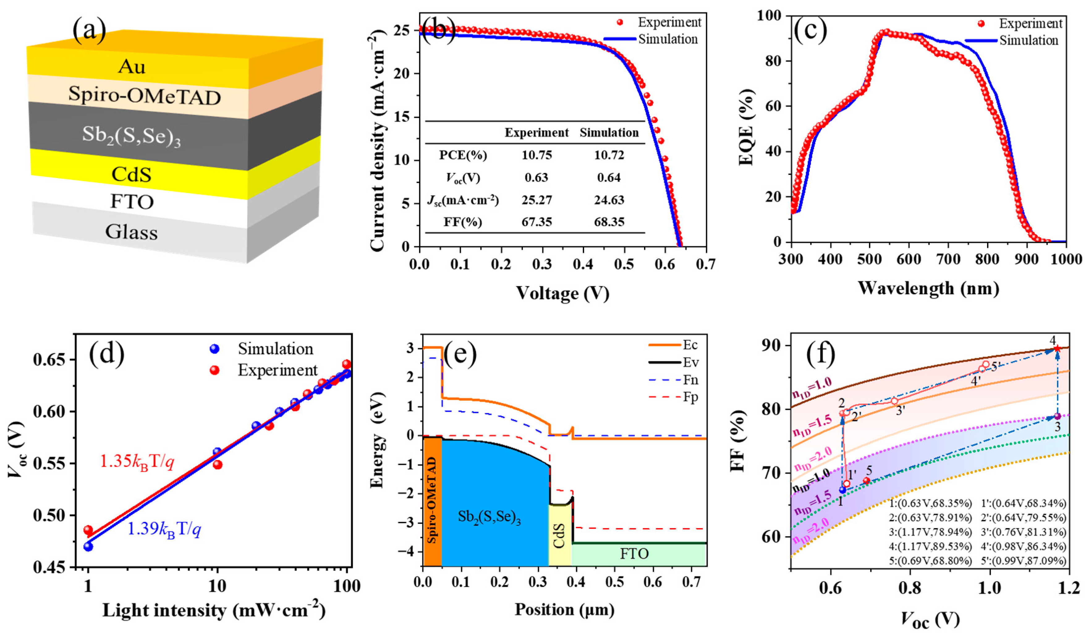
2.3. Device Validation and Optimization Route

Simulation 1 of the Sb2(S,Se)3 solar cell was established utilizing the parameters outlined in Tables S1–S3 of the Supplementary Material. When Rs = 3 Ω·cm2 and Rsh = 375 Ω·cm2, the simulation results strongly agree with the experimental findings reported in [4], particularly the current density–voltage (JV) characteristic curves and external quantum efficiency (EQE) spectra, as evident in Figure 1b,c, respectively. To further confirm the accuracy of the model, a comparative analysis was conducted on how Voc correlates with variations in light intensity. According to the data presented in Figure 1d, the ideal factor (nID) values of the experimental and simulated devices are 1.35 and 1.39, respectively, revealing strong consistency between the measurements and simulations. Additionally, an nID value between 1 and 2 indicates that interface recombination predominates in Sb2(S,Se)3 solar cells [26]. As depicted in Figure 1e, the band alignment diagram clearly illustrates that the Sb2(S,Se)3 absorber layer is fully depleted, indicating a strong electric field throughout the entire layer. This robust electric field serves as a driving force, greatly enhancing the separation efficiency of photogenerated electron–hole pairs.
In our simulated device, the Sb2(S,Se)3 absorber has an Eg of 1.43 eV, which approaches the nearly ideal bandgap (Eg = 1.34 eV) of the S–Q efficiency limit [5,27]. However, the actual device performance only reaches a maximum efficiency of 10.75%, which is significantly below the S–Q efficiency limit. For instance, at an Eg of 1.43 eV, the S–Q limit predicts a PCE of 32.54% with a Voc of 1.17 V and an FF of 89.53% [5]. A strong correlation exists between FF and Voc, where the maximum achievable FF (FFm) theoretically depends solely on Voc [3,28,29], assuming a negligibly small Rs (Rs ≈ 0) and an ideal Rsh (Rsh → ∞).
F F m = ν o c l n ( ν o c + 0.72 ) ν o c + 1 ,     w i t h   ν o c = q V o c n I D k B T
The relationship between FFm and Voc is primarily influenced by nID, which represents the nonradiative recombination rate. However, in actual devices, Rs and Rsh cannot be neglected. Rs and Rsh are considered in Equation (5), as shown in Equation (6) [30,31].
F F = F F s 1 ν o c + 0.7 ν o c   F F s r s h ,     w i t h   F F s = F F m 1 1.1 r s + r s 2 5.4 ,     r s h = J s c R s h V o c   a n d   r s = J s c R s V o c
Applying Equations (5) and (6), the FF and FFm of Sb2(S,Se)3 solar cells were determined on the basis of empirical Voc–FF plots, where the nID value was varied from 1 to 2. According to Figure 1f, with Rs = 0 Ω·cm2 and Rsh = 107 Ω·cm2, at a Voc of approximately 0.63 V (that is, from point 1 to point 2 on the graph), the calculated FF increased from 68.35% to 78.91%. On the other hand, by decreasing nID from 1.39 to 1.0, the FF increased from 68.35% at 0.63 V to 79.94% at the S–Q limit, with a Voc of 1.17 V (that is, moving from point 1 to point 3). On the basis of these findings, after the respective optimizations, the FF constrained by the internal resistance (78.91%) was lower than that constrained by the nonradiative recombination (79.94%). Consequently, within the regimes of low Voc and FF, the internal resistance exerted a more significant limiting effect on the FF than nonradiative recombination did. These results highlight the rationale behind implementing a phased strategy employing staged optimization to reduce Voc loss and FF loss in Sb2(S,Se)3 solar cells. This strategy involves initially optimizing internal resistances before addressing nonradiative recombination in Sb2(S,Se)3 solar cells (that is, from point 1 to point 2 and then to point 4, as illustrated in Figure 1f). Additionally, point 5 in Figure 1f represents the high-efficiency Sb2(S,Se)3 solar cell with the current lowest Voc loss [3], whereas points 1′–5′ represent the results from five simulated devices obtained following our designed optimization route.

3. Results and Discussion

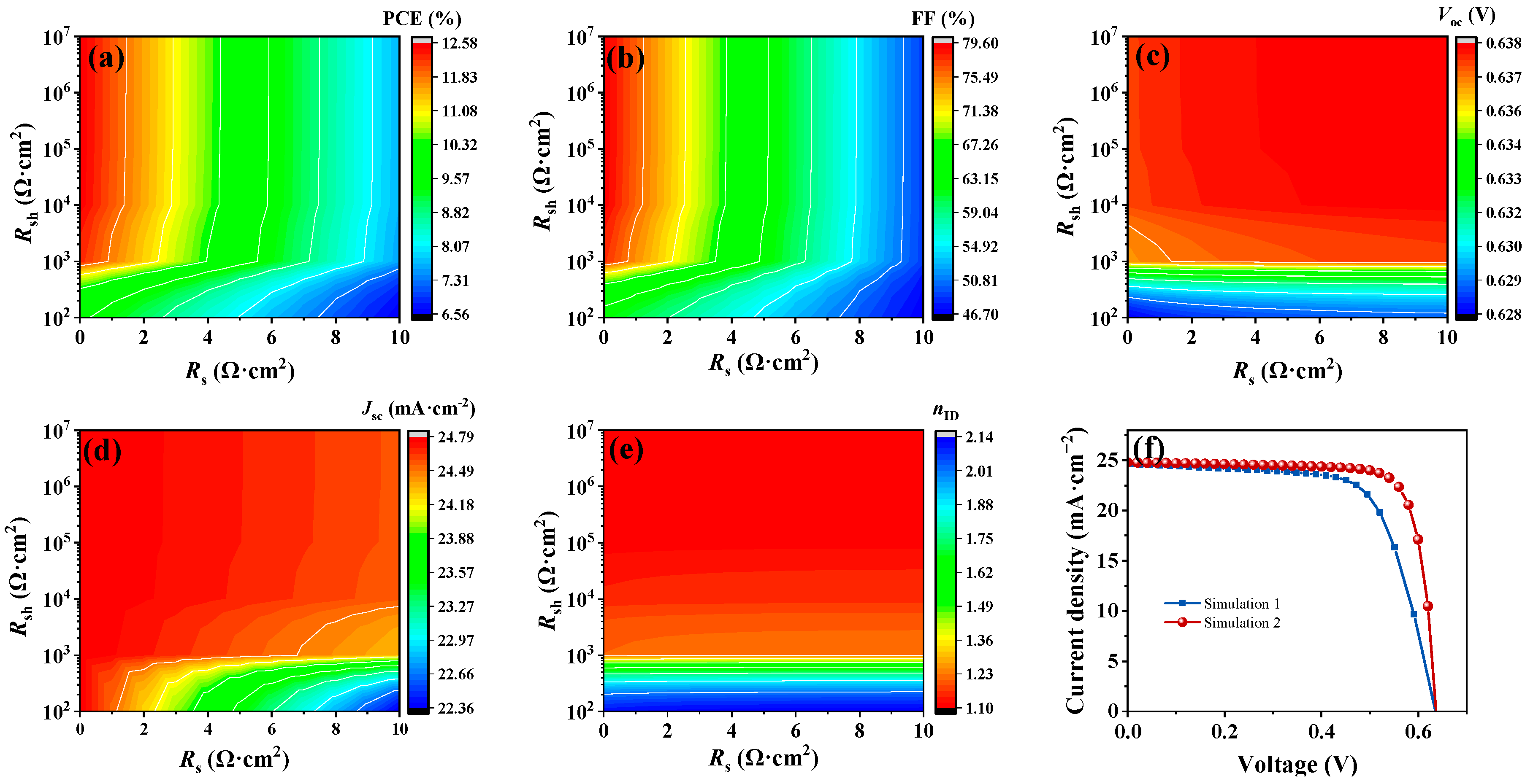
3.1. Optimization of the Series and Shunt Resistances

The series and shunt resistances are crucial factors influencing the performance of solar cells. Simulation 1 effectively replicates the experimental JV curves, EQE spectra, and ideality factor (nID), aligning closely with published data [4]. This validation highlights the predictive accuracy of subsequent simulations in predicting experimental outcomes. To explore the detailed effects of Rs and Rsh, Rs was adjusted to fall within the range of 0 to 10 Ω·cm2, and the range specified for Rsh extended from 102 to 107 Ω·cm2. The simulation calculation was carried out while the other parameters in Simulation 1 remained unchanged. As illustrated in Figure 2a–d, changes in Rs have a more pronounced effect on the PCE and FF than variations in Rsh do. When Rs decreased to 0 Ω·cm2 and Rsh was maintained at 105 Ω·cm2, the FF notably increased from 68.35% to 79.55%. Conversely, the Voc and Jsc values are least affected by changes in Rs, which is consistent with previous reports [32,33]. Moreover, Figure 2e demonstrates that nID remains stable with variations in Rs when Rsh remains constant but shifts noticeably from 2.14 to 1.10 as Rsh varies from 102 Ω·cm2 to 105 Ω·cm2. Compared with Simulation 1, the JV curve of Simulation 2 (Rs decreased to 0 Ω·cm2 and Rsh increased to 105 Ω·cm2) significantly improved the FF, whereas the PCE also increased from 10.72% to 12.57% (Figure 2f). This enhancement primarily results from a marked decrease in FF loss, decreasing from 10.79% to 2.80% as detailed in Table 1, emphasizing the critical role of Rs and Rsh optimization in enhancing solar cell performance.
The findings underscore the efficacy of a dual-pronged approach in enhancing solar cell efficiency and mitigating FF losses: reducing Rs and augmenting Rsh. An increase in Rs stems from increased electrode and charge–transfer interface resistances, whereas a decrease in Rsh is tied to reduced functional layer coverage and the proliferation of pinholes. Despite the inherent challenge of fully eradicating internal resistance, these results underscore the imperative for experimental endeavors to craft electrodes with exceptional conductivity and minimal sheet resistance, alongside strategies to diminish interface charge–transfer resistance. The key determinants of this interfacial charge transfer resistance include the electrode–semiconductor contact resistance, the bulk resistance intrinsic to the semiconductor, barriers arising from interface band offsets, and recombination losses at the interface, exacerbated by impurities and defects [34]. To increase the overall performance of Sb2(S,Se)3 solar cells to unprecedented levels, concerted optimization endeavors targeting interface band alignment, interface recombination processes, and absorber defects are of paramount importance.

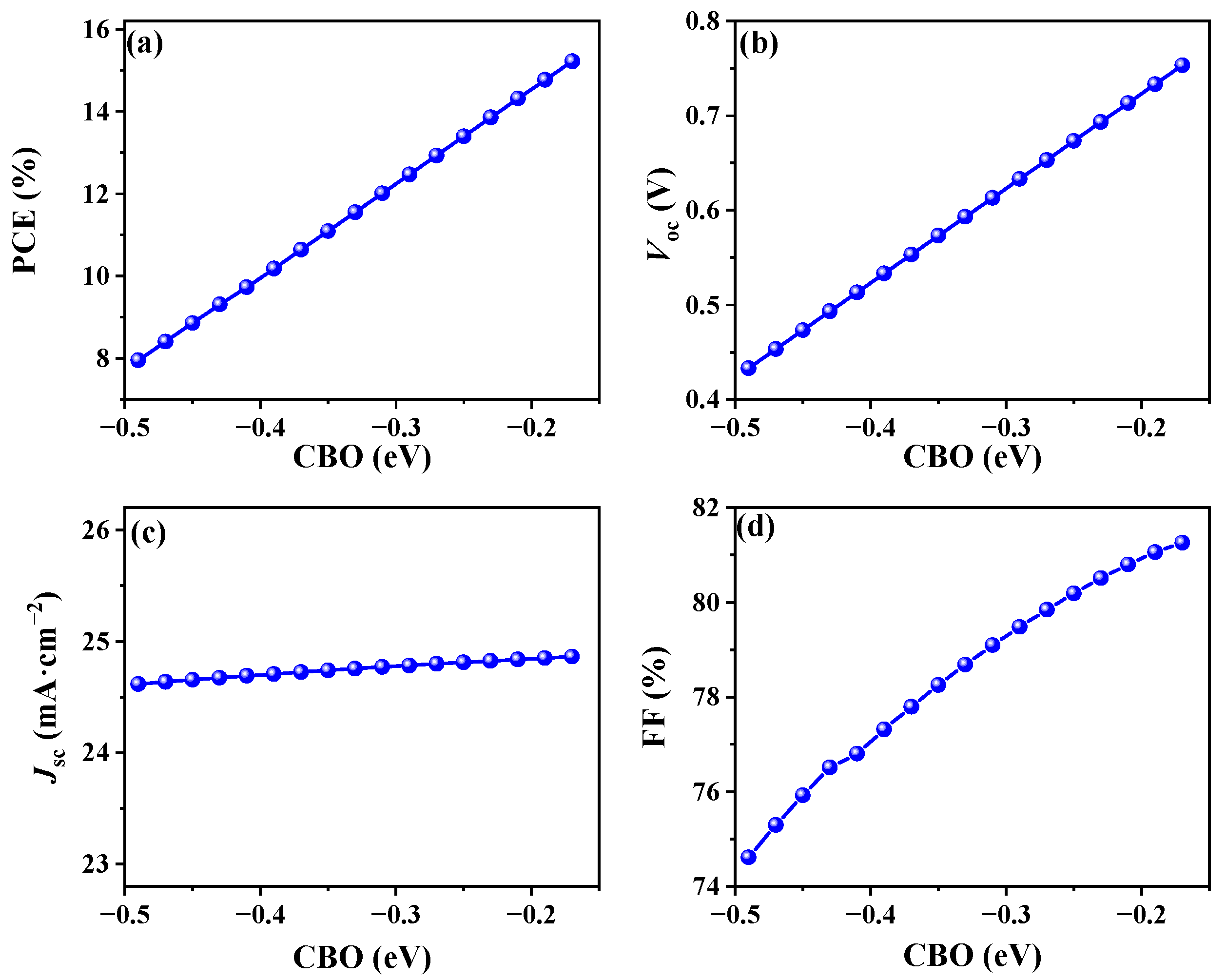
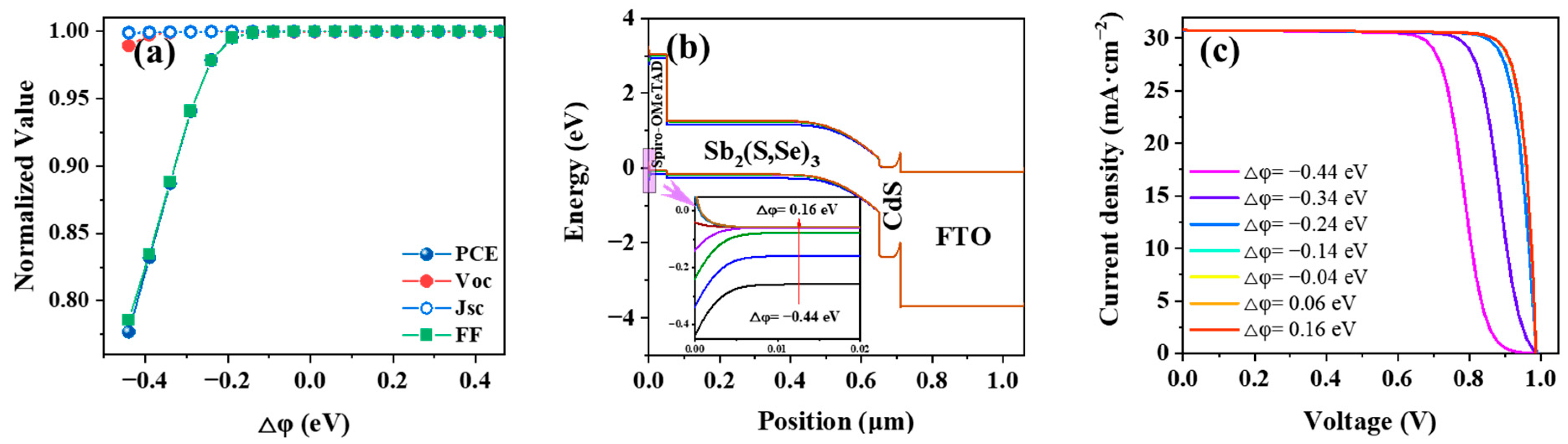
3.2. Optimization of the Energy Band Offset

Despite significant advancements in enhancing the efficiency of Sb2(S,Se)3 solar cells through meticulous optimization of the internal resistance, resulting in a notable improvement in the FF, increasing the Voc remains a formidable challenge. To overcome this obstacle, it is imperative to meticulously optimize the internal energy band arrangements within the solar cell architecture. Optimal energy level alignment can facilitate the seamless transportation of photogenerated electrons toward the front contact and holes toward the back contact, emanating from the absorber layer, thereby reducing the interface-induced recombination losses in Sb2(S,Se)3 solar cells. Establishing an ideal energy band offset (EBO) at the interfaces, which increases carrier transport properties and minimizes recombination losses, is of paramount importance [35]. Notably, the formation of EBO, a crucial aspect of Sb2(S,Se)3 solar cells, is closely linked to disparities in the electron affinity and energy gap across the material interface. Addressing these challenges through meticulous interface engineering is essential for mitigating recombination losses, enhancing Voc, and ultimately achieving higher overall efficiencies for these solar cells. The conduction band offset (CBO) existing at the junction of the ETL and absorber is fundamentally dictated by the disparity in electron affinities between these two layers ( χ a b s o r b e r   and χ E T L , respectively), as follows:
C B O = χ a b s o r b e r   χ E T L
The interface between materials can exhibit three distinct band alignment configurations, each characterized by the CBO. A negative CBO induces a steep cliff-like EBO, whereas a positive CBO yields a more pronounced spike-like EBO. When the CBO is zero, a flat band alignment is observed [36]. There is a general consensus among researchers that either a flat band alignment or a mild spike-like CBO is conducive to efficient charge transfer and the minimization of interface recombination losses [37].
Here, the band arrangements at the ETL/absorber interface were investigated by varying the χETL from 4.3 eV to 3.7 eV, with the χabsorber maintained at 3.81 eV. This range of χETL corresponded to a CBO ranging from −0.49 eV to 0.19 eV, as depicted in Figure S1a. As the CBO shifted from negative to positive values, a distinct spike-like EBO emerged in the conduction band at the ETL/absorber interface, as expected. However, a remarkable observation was made at the FTO/ETL interface, where a considerably more prominent spike-like EBO manifested in the conduction band, as clearly shown in Figure S1b. This enhanced EBO brings additional obstacles to the transfer of electrons to the front electrode, ultimately hindering charge transfer with the increase in CBO. Therefore, when CBO decreases below −0.17 eV, the electrons can surmount the potential barrier at the FTO/ETL interface and reach the front electrode, thus avoiding computational convergence issues, as shown in Figure S1c. When χ E T L was tuned from 4.3 eV to 3.98 eV (corresponding to a CBO from −0.49 eV to −0.17 eV), remarkable linear enhancements were observed in the PCE, Voc, and FF, whereas the Jsc remained relatively stable, as shown in Figure 3. This behavior originated from the reduction in cliff-like interfacial characteristics between the ETL and absorber, coupled with an enhanced built-in electric field at both the ETL/absorber and FTO/ETL interfaces (Figure S1d), resulting in reduced electron capture at the interface [38]. Thus, the Sb2(S,Se)3 solar cell reached its optimal performance at a CBO of −0.17 eV.
Certainly, the refinement of the CBO at the ETL/absorber interface significantly enhances the transport of photogenerated electrons. Nevertheless, the employment of an appropriate HTL is of paramount importance in facilitating the migration of photogenerated holes toward the back contact while simultaneously impeding the undesirable reverse flow of electrons. Thus, the valence band offset (VBO) at the interface between the absorber and HTL critically governs the transport dynamics of photogenerated holes toward the back electrode in the Sb2(S,Se)3 absorber layer. The VBO value can be calculated as follows:
VBO = E v _ absorber E v _ HTL = E g _ absorber + χ a b s o r b e r ( E g _ HTL + χ H T L )
As shown in Figure 4a, the PCE demonstrates a consistent trend of an initial rise followed by a subsequent decline at all values of NA in the HTL, when the VBO varies from −0.4 eV to 0.2 eV. This VBO variation corresponds to a range of Ev_HTL from 4.84 eV to 5.44 eV, with Ev_absorber fixed at 5.24 eV. Notably, across NA values ranging from 1016 cm−3 to 1019 cm−3, the peak PCE occurs at a VBO of −0.1 eV. In Figure 4b, the FF exhibits a similar trend to that of the PCE. However, Voc remains almost unchanged as the VBO increases to −0.1 eV, whereas Jsc initially remains constant and subsequently rapidly decreases after the VBO exceeds 0 eV (see Figure 4c,d). When the VBO exceeds 0 eV, the PCE, FF, and Jsc of the simulated device undergo rapid deterioration. This significant decline can be explained by the emergence of an energy barrier at the valence band of the absorber/HTL interface. This barrier considerably impedes the seamless flow of photogenerated holes toward the back electrode, leading to their accumulation at the interface. This accumulation, in turn, intensifies the surface recombination processes, further reducing the performance metrics of the device. When VBO is −0.1 eV (Ev_HTL = 5.14 eV) and NA ranges between 1018 cm−3 and 1019 cm−3, the device exhibits optimal performance.
As demonstrated by the simulation results, extreme positive or negative values of either the CBO or VBO adversely affect device performance. By optimizing the energy level alignment, we achieved an optimal CBO of −0.17 eV and VBO of −0.1 eV, which were applied in Simulation 3. Simulation 3 achieved a PCE of 15.31%, a Voc of 0.76 V, a Jsc of 24.86 mA·cm−2, and an FF of 81.32%. Compared with Simulation 2, the device performance in Simulation 3 showed significant improvements, with a significant reduction of 15.19% in Voc loss and a noteworthy 21.80% increase in the PCE, as detailed in Table 1. These results highlight the critical role of precise control over energy level alignment in optimizing photovoltaic device performance. To achieve this optimization while keeping the absorber material’s energy levels constant, the electron affinity of the ETL (CdS) needs to be reduced from 4.1 eV to 3.98 eV, and the electron affinity of the HTL (spiro-OMeTAD) needs to be reduced from 2.1 eV to 2.0 eV. In practice, it is necessary to optimize the conduction band energy levels of each functional layer material by adjusting doping elements or introducing specific functional groups to achieve better energy level matching, thereby constructing more efficient solar cell structures.

3.3. Optimization of Interface Recombination

Even if optimal band alignment is achieved in the device structure, the potential effect of nonradiative recombination due to interface defects resulting from lattice mismatches between functional layers must be considered. Sb2(S,Se)3 possesses an orthorhombic crystal structure, while CdS typically has a hexagonal structure and spiro-OMeTAD adopts a triclinic structure [39]. The inherent structural incompatibility among the ETL, absorber, and HTL layers leads to the emergence of lattice mismatches at their junctions, fostering the development of interface defects that act as sites for nonradiative recombination. To simulate nonradiative recombination through the Shockley–Read–Hall (SRH) mechanism, the SRH recombination rate (RSRH) is considered. The RSRH consists of three main components: bulk recombination (Rbulk) within the absorber layer, interface recombination at the ETL/absorber interface (RIF1), and interface recombination at the absorber/HTL interface (RIF2) [39,40,41], as shown in Equation (9):
R S R H = R b u l k + R I F 1 + R I F 2 = ( n p n i 2 ) σ n , p υ t h N t n + p + 2 n i c o s h E t E i k B T
where σn and σp represent the capture cross-sections for electrons and holes, respectively; υth denotes the thermal velocity; and ni and Ei represent the intrinsic density and energy level of materials, respectively. Additionally, Nt and Et are the density and energy level of the defect states, respectively, and S represents the surface recombination velocity (defined as S = σn,pυthNt).
The influence of the surface recombination velocity, namely S1 at the ETL/absorber interface and S2 at the absorber/HTL interface, on the performance parameters of Sb2(S,Se)3 solar cells is clearly illustrated in Figure 5a–d. When S2 is held constant and S1 varies between 106 and 1010 cm·s−1, the Voc remains below 0.80 V, with negligible changes in both the PCE and FF. However, when S2 is less than 104 cm·s−1 and S1 decreases from 106 to 102 cm·s−1, the PCE gradually increases, ultimately exceeding 20%, and the Voc progressively increases to nearly 1.0 V. These findings underscore the more significant impact of S1 than S2 on the Voc and PCE of Sb2(S,Se)3 solar cells. This result is likely attributed to the presence of a p–n junction formed between the p-type Sb2(S,Se)3 absorber layer and the n-type CdS layer, which governs the behavior of holes as minority carriers within the Sb2(S,Se)3 thin film. In contrast, a relatively weaker p+–p junction is formed with p-type Spiro-OMeTAD. Thus, the optimization of the ETL/absorber interface through meticulous interface engineering can likely lead to a more effective increase in the performance of Sb2(S,Se)3 solar cells [42].
Notably, Simulation 4 with optimized parameters of 102 cm·s−1 for S1 and 103 cm·s−1 for S2 attained an impressive PCE of 23.75%, with excellent characteristics, such as an nID of 1.08, a Voc loss of 0.45 V, and a negligible FF loss of 0.96%, as detailed in Table 1. As evident in Figure 5e, compared with simulation 3, optimizing the interface recombination velocities led to a notable increase in Voc from 0.76 V to 0.98 V, Jsc from 24.86 mA·cm−2 to 27.93 mA·cm−2, and PCE from 15.31% to 23.75%. Figure 5f shows that this enhancement was attributed to the improved optical response of the device at wavelengths below 600 nm after reducing interface recombination. Reducing the trap density at the ETL/absorber interface from 1014 cm−2 to 1010 cm−2 or the capture cross-section from 10−15 cm2 to 10−19 cm2 is a significant challenge for practical experiments. Indeed, interface modification engineering can passivate surface defects and improve material smoothness and surface impurities, effectively reducing trap density and/or capturing cross-sections. For example, CdS thin films etched with N2H4 exhibit higher transmittance, smoother surfaces, and fewer Cd oxychlorides [12]. Additionally, adding insulating polymer layers can further reduce surface roughness and interface states, enhancing device performance [41].

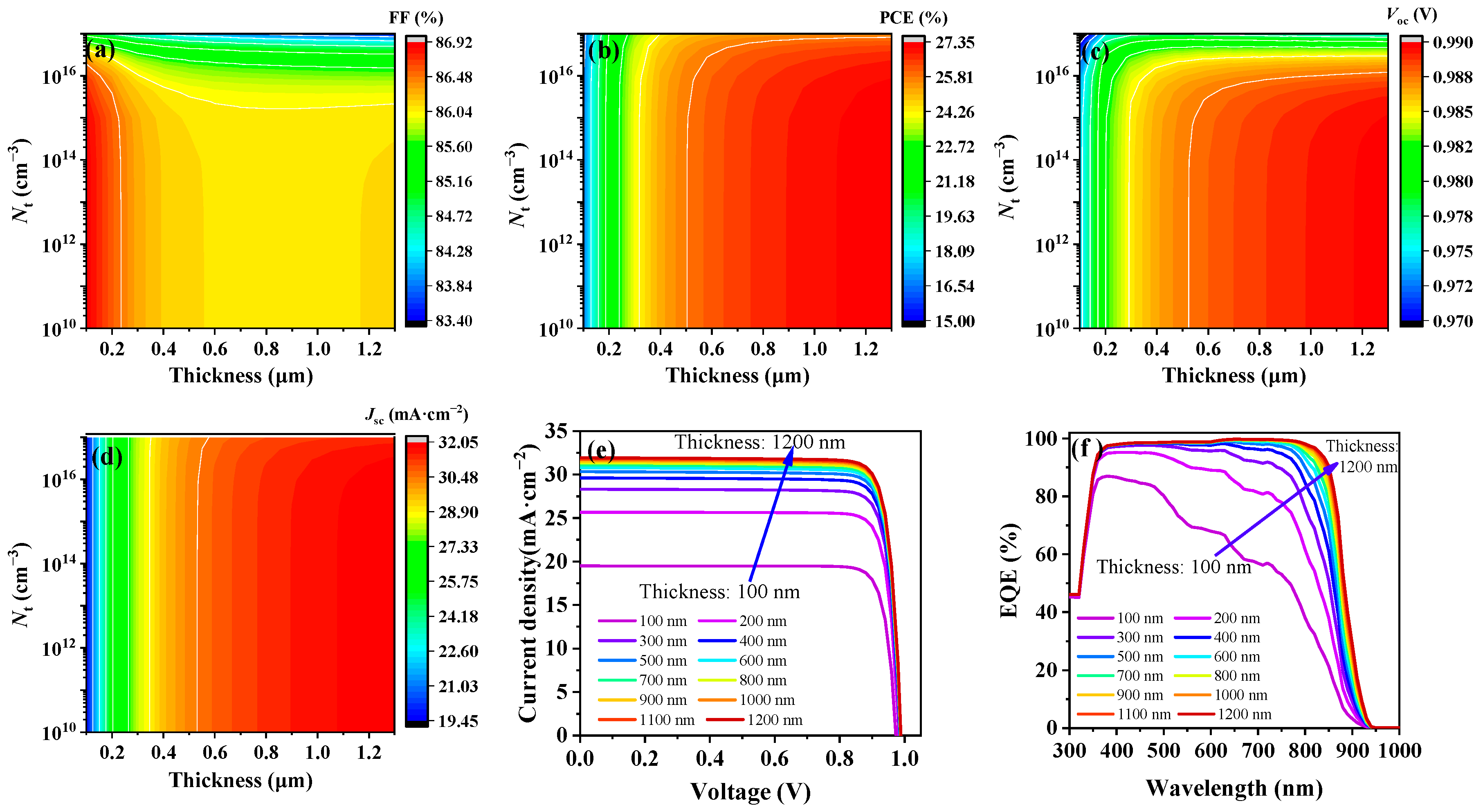
3.4. Optimization of the Sb2(S,Se)3 Absorber’s Thickness and Bulk Defects

The thickness of the Sb2(S,Se)3 absorber significantly affects various performance aspects of solar cells, including light absorption, carrier mobility, and recombination rates. Consequently, our subsequent simulations delved into the impact of varying the thickness and Nt of the absorber to pinpoint the optimal configuration for enhancing device performance. When Nt remained at 1016 cm−3 and the thickness remained below 600 nm, as evident from Figure 6a–d, there was a slight increase in Voc and a slight decrease in FF with increasing thickness, whereas both the PCE and Jsc significantly increased. The increase in absorber thickness led to greater photon absorption, resulting in a greater number of photogenerated carriers and thus improving the Jsc and PCE. However, once the thickness exceeds 600 nm, the photon absorption approaches saturation and the PCE almost plateaus, as shown in Figure 6e. Furthermore, increasing the absorber thickness from 100 nm to 1200 nm led to a significant increase in the response of the EQE (see Figure 6f). Nevertheless, this increase in absorber thickness extended the transit distance for the charge carriers before collection and elevated the internal resistance of the device, consequently reducing the FF [42]. At a thickness of 600 nm, the FF stabilized at nearly 86.01%. Consequently, with an Sb2(S,Se)3 thickness of 600 nm and an initial Nt of 6.28 × 1012 cm−3, Simulation 5 achieved a PCE of 26.77%, an FF of 87.09%, a Voc of 0.99 V, and a Jsc of 30.93 mA·cm−2, as summarized in Table 1.

3.5. Optimization of the Work Function at the Back Contact Layer

The variation in the work function of the back contact (φBC) directly impacts the energy band structure at the rear of solar cells, thereby impacting the collection of photogenerated carriers. We conducted a study to examine the influence of φBC on the performance of Sb2(S,Se)3 solar cells, with a specific focus on the difference Δφ (referred to as Ev_HTL − φBC). When Δφ ranges from −0.44 eV to 0.46 eV, φBC shifts within a range of 4.74 eV to 5.60 eV. Figure 7a reveals a consistent increasing trend in both the PCE and FF, reaching their maximum values at −0.14 eV. Beyond this Δφ value, the PCE and FF remain stable. The downward curvature in the valence band and the characteristic S-shaped curve in the current–voltage characteristics when Δφ falls below −0.14 eV, as depicted in Figure 7b,c, clarify this phenomenon. The varying energy levels across the HTL/back contact interface, causing the emergence of a Schottky barrier within the Δφ range of −0.44 eV to −0.14 eV, are responsible for impeding the unhampered flow of holes from the HTL toward the back electrode, as shown in Figure 7b. Notably, when Δφ approaches or exceeds −0.14 eV, the barrier gradually diminishes, allowing for improved hole transport and reduced resistance at the HTL/back contact interface, and all device parameters are saturated. In other words, when φBC exceeds 5.04 eV, the back electrode and HTL form a good ohmic contact conducive to hole collection. The back contact employed in Simulation 5 is gold (φBC = 5.1 eV), which falls within the optimized range, and the back contact of the Sb2(S,Se)3 solar cell can be unchanged.

3.6. Final Optimized Sb2(S,Se)3 Solar Cell Performance

After the above optimization analysis, the final values are as follow: the thickness of Sb2(S,Se)3 is 600 nm, and the electron affinities of the ETL (CdS) and HTL (spiro-OMeTAD) are optimized to 3.98 eV and 2.04 eV, respectively; the interface recombination velocities of ETL/absorber and absorber/HTL are optimized at 102 cm·s−1 and 103 cm·s−1, respectively. Additionally, the back electrode with a work function greater than 5.04 eV (e.g., Au~5.1 eV) can form a better ohmic contact with HTL, and the series and shunt resistances of the device are optimized to 0 and 105 Ω·cm2, respectively. As shown in Table 1, the final optimized device (simulation 5) has achieved excellent performance parameters: Voc = 0.99 V, Jsc = 30.93 mA·cm−2, FF = 87.09%, and PCE = 26.77%. Compared with other simulation results presented in Table S4, the performance of our simulated Sb2(S,Se)3 solar cell is superior, due to the effective optimization path chosen based on Voc and FF losses to enhance the device structure.

4. Improvement in the PCE of the Sb2(S,Se)3 Solar Cells

Based on the preceding simulation outcomes, a two-phased approach is proposed to increase the efficiency of Sb2(S,Se)3 solar cells. Initially, an efficiency benchmark of up to 15% was achieved, and subsequently, the goal was to surpass the 20% efficiency threshold.
Approaching 15% efficiency. Although the lowest Voc loss reported in Sb2(S,Se)3 solar cells has an Eg of 1.46 eV [3], the Voc value remains at approximately 0.69 V, which is notably far lower than the S–Q limit Voc of 1.19 V. This discrepancy is commonly observed in Sb2(S,Se)3 solar cells with PCEs surpassing 10% [3,4,11,13,14,15,43,44,45], highlighting a persistent challenge in their performance improvement [26]. To overcome this challenge, feasible methods for enhancing carrier transport properties, minimizing recombination losses, and improving the internal resistance of Sb2(S,Se)3 solar cells include the following:
(1)
Regulation of the absorption film to reduce the internal resistance. The Sb2(S,Se)3 compound possesses a unique quasi-1D ribbon architecture characterized by [Sb4S(e)6]n ribbons [46]. This structural peculiarity engenders favorable grain morphology and anisotropic carrier mobility, most notably along the [hk1] direction. This specific transport pathway underscores the prospect of significantly elevated device performance, particularly in comparison with transport along the [hk0] direction. Different synthesis/fabrication strategies have been used to develop [hk1]-oriented Sb2(S,Se)3 films. A highly efficient method lies in rapid hydrothermal deposition, which kinetically promotes the growth of [221]-oriented crystals [15]. Additionally, during synthesis processes such as close space sublimation (CSS) [47], rapid thermal evaporation (RTE) [45], and vapor transport deposition (VTD) [48], carefully balancing the temperature between the evaporation source and the substrate has been shown to be crucial for promoting [hk1] orientation and enhancing the crystallinity of Sb2(S,Se)3 films. High-quality crystals, characterized by low defect density, extended carrier lifetimes, elevated electron and hole mobilities, and uniform crystal structures, play a pivotal role in reducing internal resistance and optimizing carrier transport in solar cells.
(2)
Band alignment absorber layer and charge-transport layers. To fully unlock the potential of Sb2(S,Se)3 solar cells in terms of the PCE, the optimization of the carrier transport path has emerged as a paramount step forward in advancing their performance. This can be achieved through careful adjustment of CBO at the ETL/absorber interface and VBO at the absorber/HTL interfaces [49]. The proper alignment of the energy bands between the absorber layer and charge–transport layers is essential for minimizing energy-level mismatches and reducing the interface energy barriers. Optimizing the interface energy barrier involves using ETLs and HTLs with minimal defects or employing doping strategies to mitigate band mismatch. For example, nitrogen-containing functional groups in ethylenediamine (EDA) can coordinate with CdS, and shift the Fermi level of EDA–CdS toward the conduction band [50]. Alternatively, in situ oxygen doping of CdS films results in a lower conduction band level compared to that of control CdS films [51]. Various configurations of CdS-based ETLs such as SnO2/CdS [25,52], TiO2/CdS [53,54], ZnO/CdS [55], and Zn(O,S)/CdS [56] ensure well-matched band alignment, thereby facilitating efficient charge transport in Sb2(S,Se)3 solar cells.
Exceeding 20% efficiency. Reducing SRH recombination is a critical aspect of improving the performance of Sb2(S,Se)3 solar cells. By implementing appropriate passivation strategies and surface treatments, such as postselenization [57,58] and advanced interfacial engineering [59,60], it is feasible to significantly diminish the defect density within a material. This reduction not only mitigates the entrapment of charge carriers but also increases their lifetime. Achieving an efficiency of more than 20% in Sb2(S,Se)3 solar cells requires suitable methods, including the following:
(1)
Regulation of the interface recombination. Annealing and interface treatments are essential for rectifying instability, smoothing out roughness, and enhancing conductivity within ETLs. This helps minimize the defect density and lower carrier recombination at the ETL/absorber junction. For example, oxygen-doped cadmium sulfide (CdS:O) facilitates the tailoring of (Sb4S(e)6)n ribbons to the (221)-textured orientation [61], CdCl2-modified CdS films passivate surface defects [62], and KCl-treated CdS films promote absorption layer growth [10]. Furthermore, enhancing the p-type characteristics of HTL materials through doping or developing low-cost and efficient alternatives is crucial for increasing hole mobility and improving material conductivity, such as high-mobility and work-function NiOx [63,64], excellent near-infrared-absorption PbS colloidal quantum dots [7,65], and high-hole-mobility and high-stability CuSCN [66]. These alternative approaches hold significant potential in increasing the performance of solar cells, primarily through the enhancement of hole mobility and the mitigation of interface recombination.
(2)
Balance of the relationship between the thickness of the absorber and bulk defects. Both theoretical calculations [67,68,69] and experimental measurements [3,70] have demonstrated the complex defect mechanisms in Sb2(S,Se)3. The thickness of the absorber layer influences both photon absorption and carrier transport [71]. If the absorber layer is too thin, insufficient photon absorption occurs, and pinhole formation increases, thereby resulting in a low Jsc. However, during the actual preparation process, overly thick layers increase photon absorption while also increasing the series resistance and carrier transport distance, thereby intensifying carrier recombination. The thickness of the absorber layer can be controlled by adjusting the synthesis/fabrication time and growth rate. Furthermore, the absorber bulk defects are reduced through empirical methods such as adjusting the Se/S atomic ratio [15,72], postselenization treatments [73], seeding materials [74,75], or additive engineering [4,76].

5. Conclusions

In summary, a numerical model of Sb2(S,Se)3 solar cells was developed utilizing the SCAPS software (version 3.3.10; University of Gent, Belgium) package and validated against experimental data from the literature. This model was used to investigate the factors limiting Voc and FF at various stages of Sb2(S,Se)3 solar cell development, and effective strategies were identified to increase the PCE of these cells. The simulation results indicated an improvement in the PCE from 10.72% to 12.57%, as well as a significant increase in the FF from 68.35% to 79.55% after addressing the limiting mechanisms related to Rs and Rsh. Further adjustments in the CBO at the ETL/absorber and VBO at the absorber/HTL interfaces led to an increase in the PCE from 12.57% to 15.31%, along with a notable 18.75% improvement in Voc. These results highlight the importance of reducing the internal resistance to enhance the FF and show the importance of optimal energy level arrangements for increasing Voc.
The subsequent optimization of interface recombination led to a notable increase in the overall performance of Sb2(S,Se)3 solar cells, resulting in a remarkable PCE exceeding 20%. This was accompanied by a decrease in the Voc loss to 0.45 V, an increase in the Jsc to 27.93 mA·cm−2, and a reduction in the FF loss to 0.96%. These results highlight the crucial role of suppressing interface SRH recombination, particularly at the ETL/absorber interface, in improving the overall performance of devices. By striking a balance between the absorber thickness and the bulk defects, the Jsc increased to over 30 mA·cm−2 at a thickness of 600 nm, consequently increasing the PCE to an impressive 26.77%.
This numerical analysis proposes an optimization roadmap aimed at reducing Voc and FF losses, thereby successfully enhancing the efficiency of Sb2(S,Se)3 solar cells. While numerical simulations cannot completely replace experimental work, they undoubtedly provide significant guidance for future experimental efforts to improve the efficiency of Sb2(S,Se)3 solar cells, helping to avoid blind experimental exploration and thus saving valuable time and resources. Furthermore, this study proposes a two-stage strategy based on simulation results to further boost the efficiency of Sb2(S,Se)3 solar cells. We hope these findings can also be extended to other solar materials, such as Sb2Se3 and Sb2S3, thereby broadening their applicability beyond current boundaries.

Supplementary Materials

The following supporting information can be downloaded at: https://www.mdpi.com/article/10.3390/nano14171433/s1, Figure S1: (a) Energy band diagram of Sb2(S,Se)3 solar cells under different χETL, (b) The conduction band diagram of the dashed circle in (a), (c) The conduction band diagram at CBO = −0.17 eV, (d) The variation of built-in electric field at ETL/absorber and FTO/ETL interfaces with CBO varied from −0.49 eV to −0.17 eV; Table S1: Simulation parameters applied to different layers within the solar cell model; Table S2: Simulation parameters for bulk defects in Sb2(S,Se)3; Table S3: Defect parameters at the interfaces of CdS/Sb2(S,Se)3 and Sb2(S,Se)3/spiro-OMeTAD; Table S4: Performance Comparison of Sb2(S,Se)3 Solar Cells: This Work vs. Published Studies. References [3,4,9,18,19,20,21,22,23,24,25,39,77,78,79,80,81,82] are cited in the Supplementary Materials.

Author Contributions

Conceptualization, B.L.; methodology, X.X.; investigation, X.X., C.D. and G.Z.; resources, B.J. and G.Z.; validation, G.Z.; writing—original draft preparation, X.X.; writing—review and editing, C.D. and B.L.; visualization, X.X.; supervision, B.L. All authors have read and agreed to the published version of the manuscript.

Funding

This work was supported by the National Natural Science Foundation of China (Grant No. 4141004), the National Key Research and Development Program (Grant No. SQ2022YFB4200052-04B), and the Key Research and Development Program of Sichuan Province (Grant No. 2022YFG0296).

Data Availability Statement

Data will be available upon valid request.

Acknowledgments

The author thanks all SCAPS software (version 3.3.10; University of Gent, Belgium) developers at Ghent University for creating a usable software package.

Conflicts of Interest

The authors declare no conflicts of interest.

References

  1. Nicolás-Marín, M.M.; González-Castillo, J.R.; Vigil-Galán, O.; Courel, M. The state of the art of Sb2(S,Se)3 thin film solar cells: Current progress and future prospect. J. Phys. D Appl. Phys. 2022, 55, 303001. [Google Scholar] [CrossRef]
  2. Wang, J.; Li, K.; Tang, J.; Chen, C. A Perspective of Antimony Chalcogenide Photovoltaics toward Commercialization. Sol. RRL 2023, 7, 2300436. [Google Scholar] [CrossRef]
  3. Dong, J.; Liu, H.; Ding, L.; Che, B.; Xiao, P.; Cao, Z.; Liu, Y.; Lou, L.; Tang, R.; Luo, J.; et al. Lowest Open-Circuit Voltage Deficit Achievement to Attain High Efficient Antimony Selenosulfide Solar Cells. Adv. Funct. Mater. 2023, 34, 2309764. [Google Scholar] [CrossRef]
  4. Chen, X.; Che, B.; Zhao, Y.; Wang, S.; Li, H.; Gong, J.; Chen, G.; Chen, T.; Xiao, X.; Li, J. Solvent-Assisted Hydrothermal Deposition Approach for Highly-Efficient Sb2(S,Se)3 Thin-Film Solar Cells. Adv. Energy Mater. 2023, 13, 2300391. [Google Scholar] [CrossRef]
  5. Rühle, S. Tabulated values of the Shockley–Queisser limit for single junction solar cells. Sol. Energy 2016, 130, 139–147. [Google Scholar] [CrossRef]
  6. Ding, C.; Wang, D.; Liu, D.; Li, H.; Li, Y.; Hayase, S.; Sogabe, T.; Masuda, T.; Zhou, Y.; Yao, Y.; et al. Over 15% Efficiency PbS Quantum-Dot Solar Cells by Synergistic Effects of Three Interface Engineering: Reducing Nonradiative Recombination and Balancing Charge Carrier Extraction. Adv. Energy Mater. 2022, 12, 2201676. [Google Scholar] [CrossRef]
  7. Chen, C.; Wang, L.; Gao, L.; Nam, D.; Li, D.; Li, K.; Zhao, Y.; Ge, C.; Cheong, H.; Liu, H.; et al. 6.5% Certified Efficiency Sb2Se3 Solar Cells Using PbS Colloidal Quantum Dot Film as Hole-Transporting Layer. ACS Energy Lett. 2017, 2, 2125–2132. [Google Scholar] [CrossRef]
  8. Bertens, K.; Fan, J.Z.; Biondi, M.; Rasouli, A.S.; Lee, S.; Li, P.; Sun, B.; Hoogland, S.; de Arquer, F.P.G.; Lu, Z.-H.; et al. Colloidal Quantum Dot Solar Cell Band Alignment using Two-Step Ionic Doping. ACS Mater. Lett. 2020, 2, 1583–1589. [Google Scholar] [CrossRef]
  9. Zhou, R.; Li, X.; Wan, L.; Niu, H.; Wang, H.; Yang, X.; Wang, X.; Hou, J.; Xu, J.; Xu, B. Bulk Heterojunction Antimony Selenosulfide Thin-Film Solar Cells with Efficient Charge Extraction and Suppressed Recombination. Adv. Funct. Mater. 2023, 34, 2308021. [Google Scholar] [CrossRef]
  10. Liu, A.; Tang, R.; Huang, L.; Xiao, P.; Dong, Y.; Zhu, C.; Wang, H.; Hu, L.; Chen, T. KCl Treatment of CdS Electron-Transporting Layer for Improved Performance of Sb2(S,Se)3 Solar Cells. ACS Appl. Mater. Interfaces 2023, 15, 48147–48153. [Google Scholar] [CrossRef]
  11. Dong, J.; Liu, H.; Cao, Z.; Liu, Y.; Bai, Y.; Chen, M.; Liu, B.; Wu, L.; Luo, J.; Zhang, Y.; et al. Low-Cost Antimony Selenosulfide with Tunable Bandgap for Highly Efficient Solar Cells. Small 2022, 19, e2206175. [Google Scholar] [CrossRef] [PubMed]
  12. Dong, H.; Zhang, L.; Che, B.; Xiao, P.; Wang, H.; Zhu, C.; Chen, T. Hydrothermal Deposition of Antimony Selenosulfide on Titanium Oxide Nanoparticle Films for Cadmium-Free Solar Cells. ACS Appl. Opt. Mater. 2022, 1, 374–381. [Google Scholar] [CrossRef]
  13. Li, J.; Zhao, Y.; Li, C.; Wang, S.; Chen, X.; Gong, J.; Wang, X.; Xiao, X. Hydrazine Hydrate-Induced Surface Modification of CdS Electron Transport Layer Enables 10.30%-Efficient Sb2(S,Se)3 Planar Solar Cells. Adv. Sci. 2022, 9, 2202356. [Google Scholar] [CrossRef]
  14. Wang, X.; Tang, R.; Jiang, C.; Lian, W.; Ju, H.; Jiang, G.; Li, Z.; Zhu, C.; Chen, T. Manipulating the Electrical Properties of Sb2(S,Se)3 Film for High-Efficiency Solar Cell. Adv. Energy Mater. 2020, 10, 2002341. [Google Scholar] [CrossRef]
  15. Tang, R.; Wang, X.; Lian, W.; Huang, J.; Wei, Q.; Huang, M.; Yin, Y.; Jiang, C.; Yang, S.; Xing, G.; et al. Hydrothermal deposition of antimony selenosulfide thin films enables solar cells with 10% efficiency. Nat. Energy 2020, 5, 587–595. [Google Scholar] [CrossRef]
  16. Decock, K.; Zabierowski, P.; Burgelman, M. Modeling metastabilities in chalcopyrite-based thin film solar cells. J. Appl. Phys. 2012, 111, 043703. [Google Scholar] [CrossRef]
  17. Burgelman, M.; Nollet, P.; Degrave, S. Modelling polycrystalline semiconductor solar cells. Thin Solid Films 2000, 361–362, 527–532. [Google Scholar] [CrossRef]
  18. Chen, Y.; Wang, Y.; Wang, R.; Hu, X.; Tao, J.; Weng, G.-E.; Zhao, C.; Chen, S.; Zhu, Z.; Chu, J.; et al. Importance of Interfacial Passivation in the High Efficiency of Sb2Se3 Thin-Film Solar Cells: Numerical Evidence. ACS Appl. Energy Mater. 2020, 3, 10415–10422. [Google Scholar] [CrossRef]
  19. Hajjiah, A.; Gamal, M.; Kandas, I.; Gorji, N.E.; Shehata, N. DFT and AMPS-1D simulation analysis of all-perovskite solar cells based on CsPbI3/FAPbI3 bilayer structure. Sol. Energy Mater. Sol. Cells 2022, 248, 112026. [Google Scholar] [CrossRef]
  20. Xing, Y.; Guo, H.; Liu, J.; Zhang, S.; Qiu, J.; Yuan, N.; Ding, J. High-efficiency Sb2(S,Se)3 solar cells with MoO3 as a hole-transport layer. J. Alloy. Compd. 2022, 927, 166842. [Google Scholar] [CrossRef]
  21. Ngoupo, A.T.; Ouédraogo, S.; Zougmoré, F.; Ndjaka, J. Numerical analysis of ultrathin Sb2Se3-based solar cells by SCAPS-1D numerical simulator device. Chin. J. Phys. 2021, 70, 1–13. [Google Scholar] [CrossRef]
  22. Zhou, B.; Yin, X.; Zhang, J.; Zeng, G.; Li, B.; Zhang, J.; Feng, L. Numerical simulation of an innovative high efficiency solar cell with CdTe/Si composite absorption layer. Opt. Mater. 2020, 110, 110505. [Google Scholar] [CrossRef]
  23. Khadir, A. Sb2(S,Se)3-Based Thin Film Solar Cells: Numerical Investigation. Acta Phys. Pol. A 2023, 144, 52–60. [Google Scholar] [CrossRef]
  24. Mamta; Maurya, K.; Singh, V. Sb2Se3 versus Sb2S3 solar cell: A numerical simulation. Sol. Energy 2021, 228, 540–549. [Google Scholar] [CrossRef]
  25. Mao, X.; Bian, M.; Wang, C.; Zhou, R.; Wan, L.; Zhang, Z.; Zhu, J.; Chen, W.; Shi, C.; Xu, B. Ultrathin SnO2 Buffer Layer Aids in Interface and Band Engineering for Sb2(S,Se)3 Solar Cells with over 8% Efficiency. ACS Appl. Energy Mater. 2022, 5, 3022–3033. [Google Scholar] [CrossRef]
  26. Chen, C.; Tang, J. Open-Circuit Voltage Loss of Antimony Chalcogenide Solar Cells: Status, Origin, and Possible Solutions. ACS Energy Lett. 2020, 5, 2294–2304. [Google Scholar] [CrossRef]
  27. Shockley, W.; Queisser, H.J. Detailed Balance Limit of Efficiency of p-n Junction Solar Cells. J. Appl. Phys. 1961, 32, 510–519. [Google Scholar] [CrossRef]
  28. Green, M.A. Solar cell fill factors: General graph and empirical expressions. Solid-State Electron. 1981, 24, 788–789. [Google Scholar] [CrossRef]
  29. Qi, B.; Wang, J. Fill factor in organic solar cells. Phys. Chem. Chem. Phys. 2013, 15, 8972–8982. [Google Scholar] [CrossRef]
  30. Shi, J.; Zhao, C.; Yuan, J. Achieving High Fill Factor in Efficient P-i-N Perovskite Solar Cells. Small 2023, 19, e2302383. [Google Scholar] [CrossRef]
  31. Kim, H.D.; Ohkita, H. Potential Improvement in Fill Factor of Lead-Halide Perovskite Solar Cells. Sol. RRL 2017, 1, 1700027. [Google Scholar] [CrossRef]
  32. Ebon, I.R.; Ali, H.; Haque, D.; Islam, A.Z.M.T. Computational investigation towards highly efficient Sb2Se3 based solar cell with a thin WSe2 BSF layer. Eng. Res. Express 2023, 5, 045072. [Google Scholar] [CrossRef]
  33. Al Ahmed, S.R.; Sunny, A.; Rahman, S. Performance enhancement of Sb2Se3 solar cell using a back surface field layer: A numerical simulation approach. Sol. Energy Mater. Sol. Cells 2020, 221, 110919. [Google Scholar] [CrossRef]
  34. Mehmood, S.; Xia, Y.; Qu, F.; He, M. Investigating the Performance of Efficient and Stable Planer Perovskite Solar Cell with an Effective Inorganic Carrier Transport Layer Using SCAPS-1D Simulation. Energies 2023, 16, 7438. [Google Scholar] [CrossRef]
  35. Salem, M.S.; Shaker, A.; Abouelatta, M.; Alanazi, A.; Al-Dhlan, K.A.; Almurayziq, T.S. Numerical analysis of hole transport layer-free antimony selenide solar cells: Possible routes for efficiency promotion. Opt. Mater. 2022, 129, 112473. [Google Scholar] [CrossRef]
  36. Ding, C.; Zhang, Y.; Liu, F.; Kitabatake, Y.; Hayase, S.; Toyoda, T.; Yoshino, K.; Minemoto, T.; Katayama, K.; Shen, Q. Effect of the conduction band offset on interfacial recombination behavior of the planar perovskite solar cells. Nano Energy 2018, 53, 17–26. [Google Scholar] [CrossRef]
  37. Barthwal, S.; Gupta, R.; Kumar, A.; Ramesh, K.; Pathak, S.; Karak, S. Band offset engineering in antimony sulfide (Sb2S3) solar cells, using SCAPS simulation: A route toward PCE > 10%. Optik 2023, 282, 170868. [Google Scholar] [CrossRef]
  38. Chen, H.; Li, Z.-Q.; Sun, B.; Feng, X.-D. Towards high-efficiency planar heterojunction antimony sulfide solar cells. Opt. Mater. 2021, 121, 111556. [Google Scholar] [CrossRef]
  39. Ayala-Mató, F.; Vigil-Galán, O.; Nicolás-Marín, M.M.; Courel, M. Study of loss mechanisms on Sb2(S1−xSex)3 solar cell with n–i–p structure: Toward an efficiency promotion. Appl. Phys. Lett. 2021, 118, 073903. [Google Scholar] [CrossRef]
  40. Wang, D.; Li, Y.; Yang, Y.; Hayase, S.; Wu, H.; Wang, R.; Ding, C.; Shen, Q. How to minimize voltage and fill factor losses to achieve over 20% efficiency lead chalcogenide quantum dot solar cells: Strategies expected through numerical simulation. Appl. Energy 2023, 341, 121124. [Google Scholar] [CrossRef]
  41. Wang, A.; Wang, X.; Chen, Y. Investigation of the fundamental working mechanism for high-performance Sb2(S1−xSex)3 solar cells. Eur. Phys. J. Plus 2022, 137, 1085. [Google Scholar] [CrossRef]
  42. Li, Z.-Q.; Ni, M.; Feng, X.-D. Simulation of the Sb2Se3 solar cell with a hole transport layer. Mater. Res. Express 2019, 7, 016416. [Google Scholar] [CrossRef]
  43. Zhao, Y.; Wang, S.; Jiang, C.; Li, C.; Xiao, P.; Tang, R.; Gong, J.; Chen, G.; Chen, T.; Li, J.; et al. Regulating Energy Band Alignment via Alkaline Metal Fluoride Assisted Solution Post-Treatment Enabling Sb2(S,Se)3 Solar Cells with 10.7% Efficiency. Adv. Energy Mater. 2021, 12, 2103015. [Google Scholar] [CrossRef]
  44. Che, B.; Cai, Z.; Xiao, P.; Li, G.; Huang, Y.; Tang, R.; Zhu, C.; Yang, S.; Chen, T. Thermally Driven Point Defect Transformation in Antimony Selenosulfide Photovoltaic Materials. Adv. Mater. 2022, 35, e2208564. [Google Scholar] [CrossRef] [PubMed]
  45. Gao, J.; Che, B.; Cai, H.; Xiao, P.; Zhang, L.; Cai, Z.; Zhu, C.; Tang, R.; Chen, T. Single-source thermal evaporation converts anion controllable Sb2(S,Se)3 film for fabricating high-efficiency solar cell. Sci. China Mater. 2023, 66, 3415–3423. [Google Scholar] [CrossRef]
  46. Huang, M.; Cai, Z.; Chen, S. Quasi-one-dimensional Sb2(S,Se)3 alloys as bandgap-tunable and defect-tolerant photocatalytic semiconductors. J. Chem. Phys. 2020, 153, 014703. [Google Scholar] [CrossRef] [PubMed]
  47. Li, K.; Xie, Y.; Zhou, B.; Li, X.; Gao, F.; Xiong, X.; Li, B.; Zeng, G.; Ghali, M. Fabrication of closed-space sublimation Sb2(S1-xSex)3 thin-film based on a single mixed powder source for photovoltaic application. Opt. Mater. 2021, 122, 111659. [Google Scholar] [CrossRef]
  48. Zhang, L.; Bai, X.; Cui, X.; Zhang, M. Vapor transport deposited Sb2(S,Se)3 thin film: Effect of deposition temperature and Sb2S3/Sb2Se3 mass ratio. J. Cryst. Growth 2023, 622, 127385. [Google Scholar] [CrossRef]
  49. Zhao, Y.; Chen, X.; Li, J.; Xiao, X. A Review of Carrier Transport in High-Efficiency Sb2(S,Se)3 Solar Cells. Sol. RRL 2023, 7, 2300565. [Google Scholar] [CrossRef]
  50. Gu, Y.; Liang, W.; Che, Y.; Cai, Z.; Xiao, P.; Yang, J.; Zang, R.; Wang, H.; Wu, X.; Chen, T. Solvent Annealing Enabling Reconstruction of Cadmium Sulfide Film for Improved Heterojunction Quality and Photovoltaic Performance of Antimony Selenosulfide Solar Cells. Adv. Funct. Mater. 2023, 34, 2311577. [Google Scholar] [CrossRef]
  51. Li, K.; Cai, Z.; Yang, J.; Wang, H.; Zhang, L.; Tang, R.; Zhu, C.; Chen, T. Molecular Beam Epitaxy Deposition of In Situ O-Doped CdS Films for Highly Efficient Sb2(S,Se)3 Solar Cells. Adv. Funct. Mater. 2023, 33, 2304141. [Google Scholar] [CrossRef]
  52. Shi, X.; Zhang, F.; Dai, S.; Zeng, P.; Qu, J.; Song, J. Nanorod-textured Sb2(S,Se)3 bilayer with enhanced light harvesting and accelerated charge extraction for high-efficiency Sb2(S,Se)3 solar cells. Chem. Eng. J. 2022, 437, 135341. [Google Scholar] [CrossRef]
  53. Wang, W.; Wang, X.; Chen, G.; Chen, B.; Cai, H.; Chen, T.; Chen, S.; Huang, Z.; Zhu, C.; Zhang, Y. Promising Sb2(S,Se)3 Solar Cells with High Open Voltage by Application of a TiO2/CdS Double Buffer Layer. Sol. RRL 2018, 2, 1800208. [Google Scholar] [CrossRef]
  54. Wu, C.; Jiang, C.; Wang, X.; Ding, H.; Ju, H.; Zhang, L.; Chen, T.; Zhu, C. Interfacial Engineering by Indium-Doped CdS for High Efficiency Solution Processed Sb2(S1−xSex)3 Solar Cells. ACS Appl. Mater. Interfaces 2018, 11, 3207–3213. [Google Scholar] [CrossRef] [PubMed]
  55. Ishaq, M.; Deng, H.; Yuan, S.; Zhang, H.; Khan, J.; Farooq, U.; Song, H.; Tang, J. Efficient Double Buffer Layer Sb2(SexS1−x)3 Thin Film Solar Cell Via Single Source Evaporation. Sol. RRL 2018, 2, 1800144. [Google Scholar] [CrossRef]
  56. Zhao, Y.; Li, C.; Niu, J.; Zhi, Z.; Chen, G.; Gong, J.; Li, J.; Xiao, X. Zinc-based electron transport materials for over 9.6%-efficient S-rich Sb2(S,Se)3 solar cells. J. Mater. Chem. A 2021, 9, 12644–12651. [Google Scholar] [CrossRef]
  57. Rijal, S.; Adhikari, A.; Awni, R.A.; Xiao, C.; Li, D.-B.; Dokken, B.; Ellingson, A.; Flores, E.; Bista, S.S.; Pokhrel, D.; et al. Post-Annealing Treatment on Hydrothermally Grown Antimony Sulfoselenide Thin Films for Efficient Solar Cells. Sol. RRL 2022, 7, 2201009. [Google Scholar] [CrossRef]
  58. Lin, Y.-C.; Chang, C.-H.; Hung, Y.-J. Bandgap grading via sputtering and post-selenization using SeS2 powder enabling Sb2(S,Se)3 solar cells with 7.1% efficiency. Sol. Energy Mater. Sol. Cells 2023, 259, 112464. [Google Scholar] [CrossRef]
  59. Wang, C.; Li, D.; Mao, X.; Wan, L.; Cheng, Z.; Zhu, J.; Hoye, R.L.Z.; Zhou, R. Interfacial defect healing of In2S3/Sb2(S,Se)3 heterojunction solar cells with a novel wide-bandgap InOCl passivator. J. Mater. Chem. A 2023, 11, 19914–19924. [Google Scholar] [CrossRef]
  60. Pan, X.; Pan, Y.; Wang, L.; Zhao, C.; Hu, X.; Jiang, J.; Yang, B.; Chen, S.; Yang, P.; Chu, J.; et al. Interfacial engineering by applying double CdS structure electron transport layer for high-performance Sb2(S,Se)3 solar cells. Ceram. Int. 2023, 49, 22471–22478. [Google Scholar] [CrossRef]
  61. Dong, J.; Liu, Y.; Wang, Z.; Zhang, Y. Boosting VOC of antimony chalcogenide solar cells: A review on interfaces and defects. Nano Sel. 2021, 2, 1818–1848. [Google Scholar] [CrossRef]
  62. Han, X.; Shi, C.; Huang, Y.; Lv, K.; Chen, W.; Guo, F.; Wang, Y. Precise Preparation of CdS Thin Films for Efficient Sb2S3–ySey Thin-Film Solar Cells. ACS Appl. Energy Mater. 2023, 6, 6311–6316. [Google Scholar] [CrossRef]
  63. Huang, S.; Xing, Y.; Zhu, H.; Zhang, T.; Geng, K.; Yang, Y.; Zhang, H.; Gu, Q.; Qiu, J.; Jiang, S.; et al. Enhancement in the efficiency of Sb2(S,Se)3 thin-film solar cells with spin-coating NiOx as the hole transport layer. J. Mater. Chem. C 2024, 12, 3098–3104. [Google Scholar] [CrossRef]
  64. Li, J.; Hu, X.; Zheng, X.; Gao, Z.; Wang, S.; Liu, Y.; Wang, C.; Shao, W.; Fang, G. Stability and Efficiency Enhancement of Antimony Selenosulfide Solar Cells with Inorganic SnS-Modified Nickel Oxide Hole Transport Materials. Energy Technol. 2023, 12, 2300694. [Google Scholar] [CrossRef]
  65. Wei, Y.; Ding, C.; Shi, G.; Bi, H.; Li, Y.; Li, H.; Liu, D.; Yang, Y.; Wang, D.; Chen, S.; et al. Stronger Coupling of Quantum Dots in Hole Transport Layer Through Intermediate Ligand Exchange to Enhance the Efficiency of PbS Quantum Dot Solar Cells. Small Methods 2024, 2400015. [Google Scholar] [CrossRef] [PubMed]
  66. Li, K.; Wang, S.; Chen, C.; Kondrotas, R.; Hu, M.; Lu, S.; Wang, C.; Chen, W.; Tang, J. 7.5% n–i–p Sb2Se3 solar cells with CuSCN as a hole-transport layer. J. Mater. Chem. A 2019, 7, 9665–9672. [Google Scholar] [CrossRef]
  67. Zhang, B.; Qian, X. Competing Superior Electronic Structure and Complex Defect Chemistry in Quasi-One-Dimensional Antimony Chalcogenide Photovoltaic Absorbers. ACS Appl. Energy Mater. 2022, 5, 492–502. [Google Scholar] [CrossRef]
  68. Savory, C.N.; Scanlon, D.O. The complex defect chemistry of antimony selenide. J. Mater. Chem. A 2019, 7, 10739–10744. [Google Scholar] [CrossRef]
  69. Huang, M.; Xu, P.; Han, D.; Tang, J.; Chen, S. Complicated and Unconventional Defect Properties of the Quasi-One-Dimensional Photovoltaic Semiconductor Sb2Se3. ACS Appl. Mater. Interfaces 2019, 11, 15564–15572. [Google Scholar] [CrossRef]
  70. Huang, Y.; Tang, R.; Wang, G.; Li, G.; Che, B.; Wang, Y.; Lian, W.; Zhu, C.; Chen, T. Chemical insight into the hydrothermal deposition of Sb2(S,Se)3 towards delicate microstructure engineering. J. Mater. Chem. A 2022, 10, 9892–9901. [Google Scholar] [CrossRef]
  71. Wu, M.; Han, N.; Chen, Y.; Zeng, H.; Li, X. Performance investigation of antimony chalcogenide based thin film solar cells via SCAPS simulation. Optik 2023, 272, 170393. [Google Scholar] [CrossRef]
  72. Wang, R.; Qin, D.; Zheng, S.; Weng, G.; Hu, X.; Tao, J.; Chu, J.; Akiyama, H.; Chen, S. Influence of S-content ratios on the defect properties of Sb2(S, Se1–)3 thin-film solar cells. Sol. Energy Mater. Sol. Cells 2023, 260, 112501. [Google Scholar] [CrossRef]
  73. Chen, G.-J.; Tang, R.; Chen, S.; Zheng, Z.-H.; Su, Z.-H.; Ma, H.-L.; Zhang, X.-H.; Fan, P.; Liang, G.-X. Crystal Growth Promotion and Defect Passivation by Hydrothermal and Selenized Deposition for Substrate-Structured Antimony Selenosulfide Solar Cells. ACS Appl. Mater. Interfaces 2022, 14, 31986–31997. [Google Scholar] [CrossRef]
  74. Zhang, L.; Lian, W.; Zhao, X.; Yin, Y.; Chen, T.; Zhu, C. Sb2S3 Seed-Mediated Growth of Low-Defect Sb2S3 on a TiO2 Substrate for Efficient Solar Cells. ACS Appl. Energy Mater. 2020, 3, 12417–12422. [Google Scholar] [CrossRef]
  75. Amin, A.; Li, D.; Duan, X.; Vijayaraghavan, S.N.; Menon, H.G.; Wall, J.; Weaver, M.; Cheng, M.M.; Zheng, Y.; Li, L.; et al. Enhanced Efficiency and Stability in Sb2S3 Seed Layer Buffered Sb2Se3 Solar Cells. Adv. Mater. Interfaces 2022, 9, 2200547. [Google Scholar] [CrossRef]
  76. Baron-Jaimes, A.; Ortiz-Soto, K.A.; Millán-Franco, M.A.; Gamboa, R.A.M.; Rincón, M.E.; Jaramillo-Quintero, O.A. Additive engineering by tetrabutylammonium iodide for antimony selenosulfide solar cells. J. Phys. D Appl. Phys. 2023, 56, 485501. [Google Scholar] [CrossRef]
  77. Mamta; Kumari, R.; Maurya, K.; Singh, V. Sb2(S,Se)3-based photovoltaic cell with MoS2 as a hole transport layer: A numerical investigation. Mater. Today Sustain. 2022, 20, 100218. [Google Scholar] [CrossRef]
  78. Nicolás-Marín, M.; Ayala-Mato, F.; Vigil-Galán, O.; Courel, M. Simulation analysis of Cd1−xZnxS/Sb2(Se1−xSx)3 solar cells with n-i-p structure. Sol. Energy 2021, 224, 245–252. [Google Scholar] [CrossRef]
  79. Nicolás-Marín, M.M.; Vigil-Galán, O.; Ayala-Mato, F.; Courel, M. Analysis of Hole Transport Layer and Electron Transport Layer Materials in the Efficiency Improvement of Sb2(Se1−xSx)3 Solar Cell. Phys. Status Solidi (B) 2022, 260, 2200342. [Google Scholar] [CrossRef]
  80. Sekar, K.; Mayarambakam, S. Effect of Annealed and Non-Annealed Inorganic MnS Hole-Transport Layer for Efficient Sb2(S,Se)3 Solar Cells: A Theoretical Justification. Phys. Status Solidi (B) 2023, 260, 2300087. [Google Scholar] [CrossRef]
  81. Gharibshahian, I.; Orouji, A.A.; Sharbati, S. Efficient Sb2(S,Se)3/Zn(O,S) solar cells with high open-circuit voltage by controlling sulfur content in the absorber-buffer layers. Sol. Energy 2021, 227, 606–615. [Google Scholar] [CrossRef]
  82. Barthwal, S.; Singh, S.; Chauhan, A.K.; Karuppannan, R. Design and Simulation of CdS-Free Sb2(S, Se)3 Solar Cells with Efficiency Exceeding 20%. ACS Sustain. Chem. Eng. 2023, 12, 947–958. [Google Scholar] [CrossRef]
Figure 1. (a) Schematic illustrations depicting the simulated device. (b) JV curves, (c) EQE spectra, and (d) the ideal factor (nID) comparison between the experimental and simulated devices. (e) Energy band structure of the Sb2(S,Se)3 solar cell. (f) The FFm (solid lines) and FF (dotted lines) versus Voc for different nID values. Experimental data from the literature [4].
Nanomaterials 14 01433 g001
Figure 2. Simulated results for (a) PCE, (b) FF, (c) Voc, (d) Jsc, and (e) nID with varying Rs and Rsh. (f) The JV curves for Simulation 1 versus Simulation 2.
Nanomaterials 14 01433 g002
Figure 3. Simulation results for (a) PCE, (b) Voc, (c) Jsc, and (d) FF with varied CBO from −0.49 to −0.17 eV (χETL from 3.86 to 4.30 eV). Other parameters are based on Simulation 2.
Nanomaterials 14 01433 g003
Figure 4. Simulation results for (a) PCE, (b) Voc, (c) Jsc, and (d) FF as a function of varied VBO (−0.4 eV to 0.2 eV).
Nanomaterials 14 01433 g004
Figure 5. Simulated results for (a) PCE, (b) Voc, (c) Jsc, and (d) FF as a function of varied S1 and S2. (e) J–V curves and (f) EQE spectra for Simulation 3 and Simulation 4.
Nanomaterials 14 01433 g005
Figure 6. Simulated results for (a) FF, (b) PCE, (c) Voc, and (d) Jsc with varied Nt and thickness of the Sb2(S,Se)3 layer. (e) JV curves and (f) EQE spectra with varied thickness of the Sb2(S,Se)3 layer.
Nanomaterials 14 01433 g006
Figure 7. (a) The influence of Δφ on device performance, (b) the energy band diagrams, and (c) JV curses with varied Δφ from −0.44 eV to 0.16 eV.
Nanomaterials 14 01433 g007
Table 1. Photovoltaic parameters in five simulated devices.
Voc (V)FF (%)Voc Losst (a) (V)FF Loss (b) (%)nIDJsc (mA·cm−2)PCE (%)
Simulation 10.6468.350.7910.791.3924.6310.72
Simulation 20.6479.550.792.801.1024.7912.57
Simulation 30.7681.310.673.021.1124.8615.31
Simulation 40.9886.340.450.961.0827.9323.75
Simulation 50.9987.090.440.311.0830.9326.77
(a) Voc loss is equal to Eg/qVoc, where Eg represents the bandgap of the active absorber and q is the elementary charge. (b) FF loss is equal to FFm − FF, where FFm denotes the maximum achievable FF across varying Voc values in a single solar cell.
Disclaimer/Publisher’s Note: The statements, opinions and data contained in all publications are solely those of the individual author(s) and contributor(s) and not of MDPI and/or the editor(s). MDPI and/or the editor(s) disclaim responsibility for any injury to people or property resulting from any ideas, methods, instructions or products referred to in the content.

