Article

A Hybrid Perovskite-Based Electromagnetic Wave Absorber with Enhanced Conduction Loss and Interfacial Polarization through Carbon Sphere Embedding

1
Field Engineering College, Army Engineering University of PLA, Nanjing 210007, China
2
State Key Laboratory for Disaster Prevention & Mitigation of Explosion & Impact, Army Engineering University of PLA, Nanjing 210007, China
3
Electromagnetic Environmental Effects Laboratory, Army Engineering University of PLA, Nanjing 210007, China
4
Position Engineering Research Office, Army Engineering University of PLA, Nanjing 210007, China
*
Authors to whom correspondence should be addressed.
These authors contributed equally to this work.
Nanomaterials 2024, 14(19), 1566; https://doi.org/10.3390/nano14191566
Submission received: 26 August 2024 / Revised: 21 September 2024 / Accepted: 26 September 2024 / Published: 27 September 2024

Abstract

:
Electronic equipment brings great convenience to daily life but also causes a lot of electromagnetic radiation pollution. Therefore, there is an urgent demand for electromagnetic wave-absorbing materials with a low thickness, wide bandwidth, and strong absorption. This work obtained a high-performance electromagnetic wave absorption system by adding conductive carbon spheres (CSs) to the CH3NH3PbI3 (MAPbI3) absorber. In this system, MAPbI3, with strong dipole and relaxation polarization, acts dominant to the wave absorber. The carbon spheres provide a free electron transport channel between MAPbI3 lattices and constructs interfacial polarization loss in MAPbI3/CS. By regulating the content of CSs, we speculate that this increased effective absorption bandwidth and reflection loss intensity are attributed to the conductive channel of the carbon sphere and the interfacial polarization. As a result, when the mass ratio of the carbon sphere is 7.7%, the reflection loss intensity of MAPbI3/CS reaches −54 dB at 12 GHz, the corresponding effective absorption bandwidth is 4 GHz (10.24–14.24 GHz), and the absorber thickness is 2.96 mm. This work proves that enhancing conduction loss and interfacial polarization loss is an effective strategy for regulating the properties of dielectric loss-type absorbing materials. It also indicates that organic-inorganic hybrid perovskites have great potential in the field of electromagnetic wave absorption.

1. Introduction

Studying new electromagnetic absorbing materials with effective absorption bandwidths is urgent to cope with the electromagnetic interference and radiation caused by electronic equipment [1,2,3,4,5,6]. In recent years, organic-inorganic hybrid perovskite has been proven to be a potential wave-absorber because of its high element tolerance, changeable lattice structure, and mild solution preparation methods [7,8,9,10,11]. However, problems such as relatively low absorption intensity (−3.3 dB) and large thickness of the absorber (4 mm) limit the in-depth application of hybrid perovskites in the field of electromagnetic wave absorption [8]. It has been found that preparing multi-component composites, enhancing polarization, and constructing multiple loss mechanisms are important ways of adjusting the impedance matching of absorbing materials [12,13,14,15,16,17,18,19,20,21,22]. Therefore, how to design a perovskite-based absorbing system with a precisely tunable composition and structure to improve reflection loss and absorption bandwidth is an urgent problem to be solved.
Meanwhile, the carbon sphere (CS) has become an ideal wave-shielding matrix due to its high conductivity, low density, and stable structure [23,24]. The surficial porous structure of the CS can reflect and scatter the incident electromagnetic wave multiple times, enhancing the attenuation of incident electromagnetic waves. Ji et al. prepared mesoporous CSs by hard template etching, adjusted the mesoporous size, and obtained a maximum reflection loss of −50.9 dB [25]; Han et al. reported a Mo2C@C nanosphere. By utilizing multiple loss mechanisms such as conductivity loss, dipole polarization loss, and interfacial polarization loss, the reflection loss at 12.5 GHz reaches −48.0 dB, and the effective absorption bandwidth is 3.5–18.0 GHz [26]. Therefore, through combining CSs with other wave-absorbing materials, the polarization loss intensity of the wave-absorbing system can be improved by taking advantage of its characteristics, such as the adjustable shape and size and the large specific surface area of CSs. Meanwhile, CSs can form conductive networks in the composite wave-absorbing system, increasing conductivity loss intensity.
This work uses CH3NH3PbI3 (MAPbI3) as the host to composite porous CSs to construct MAPbI3/CS. We obtained an optimal reflection loss intensity of −54 dB and an effective absorption bandwidth of 4 GHz (10.24–14.24 GHz) when the absorbent’s additive amount was 40 wt% and the mass ratio of MAPbI3:CS was 12:1. Further analyzing the internal polarization relaxation process of composites, we found that the introduction of CSs enhances the interfacial polarization and impedance matching of the system. As a result, it improved the intensity of polarization loss. At the same time, the high conductivity of the CSs improved the dielectric loss intensity of the system. Through this work, we explored the influence of the content of CSs on the absorbing properties of a MAPbI3/CS composite, which laid a foundation for the design and preparation of high-performance perovskite-based absorbing materials.

2. Materials and Methods

2.1. Synthesis of MAPbI3 Microcrystals and Carbon Sphere

MAPbI3 was synthesized by an anti-solvent method [8]. The CS material was obtained by carbonizing phenolic resin balls with phenolic resin balls as precursors. Phenolic resin spheres were prepared by suspension polymerization. First, 0.9 g of 3-aminophenol was fully dissolved in a mixed solution of deionized water and ethanol, and the deionized water and ethanol solutions were of 60 mL and 25 mL, respectively. Then, 0.27 mL of ammonia water was added dropwise to the mixed solution under stirring, and we continued to add 1.215 mL of formaldehyde solution dropwise after the solution was stable. The mixed solution was continuously stirred for 4 h, and then the mixed solution was centrifuged and washed several times with deionized water and ethanol, and the obtained milky white material was the phenolic resin ball precursor. Finally, the dried phenolic resin ball precursor was put into a tubular high-temperature heating furnace for annealing treatment. The annealing temperature was 800 °C, the holding time was 3 h, and argon was used as the atmosphere condition. The black powder after the annealing treatment was the CSs.

2.2. Synthesis of MAPbI3/CS Composites

A CS suspension was prepared by dispersing CS powder in γ-butyrolactone solution at a concentration of 30 mg/mL, and then stirring at 25 °C for 3 h. Then, the MAPbI3 precursor solution and the CS suspension were mixed according to a certain proportion and stirred at 25 °C for 1 h. According to the mass ratios of 24:1, 16:1, 12:1, 8:1, and 6:1 (MAPbI3 versus CSs), the MAPbI3/CS composites were prepared and marked as MS-1, MS-2, MS-3, MS-4, and MS-5, respectively. After the reaction, the MAPbI3/CS mixed solution was quickly added dropwise into the excess anisole solution. A large amount of black suspended solids could be observed during the reaction. Then, the anisole solution was placed under a nitrogen atmosphere for 12 h. Finally, the lower precipitate in anisole solution was washed by centrifugation with isopropanol and n-hexane several times, and the resulting product was dried under vacuum at 80 °C for 24 h. The obtained black sample was the MAPbI3/CS composite.

2.3. Structural Characterization

XRD analysis was carried out using a D8 Advance X-ray diffractometer. The operating voltage of the instrument was 50 KV, the operating current was 100 mA, and the Cu target Kα ray ( λ = 1.54187   ) test range was 2θ = 5–80°. Raman analysis was carried out using an Acutech Scientific 1500 RAMAN spectrometer (Arcadia, CA, USA). Photoluminescence (PL) analysis was conducted by FLS-1000, and the wavelength range of the samples was 200–800 nm. SEM analysis was carried out using the Nova NanoSEM 450 instrument (FEI, Eindhoven, The Netherlands).

2.4. Material Microwave Absorption Characterization

The electromagnetic parameters were tested via a PNA N5244A vector network analyzer using the coaxial ring method. The frequency range of the test electromagnetic wave was 2–18 GHz, and the step size was 0.02 GHz. Then, the sample/paraffin mixture in a mass ratio of 2:3 was pressed into a ring specimen with an outer diameter of 7 mm and an inner diameter of 3.04 mm using a mold. Finally, the coaxial ring was put into the vector network analyzer for testing [27,28].

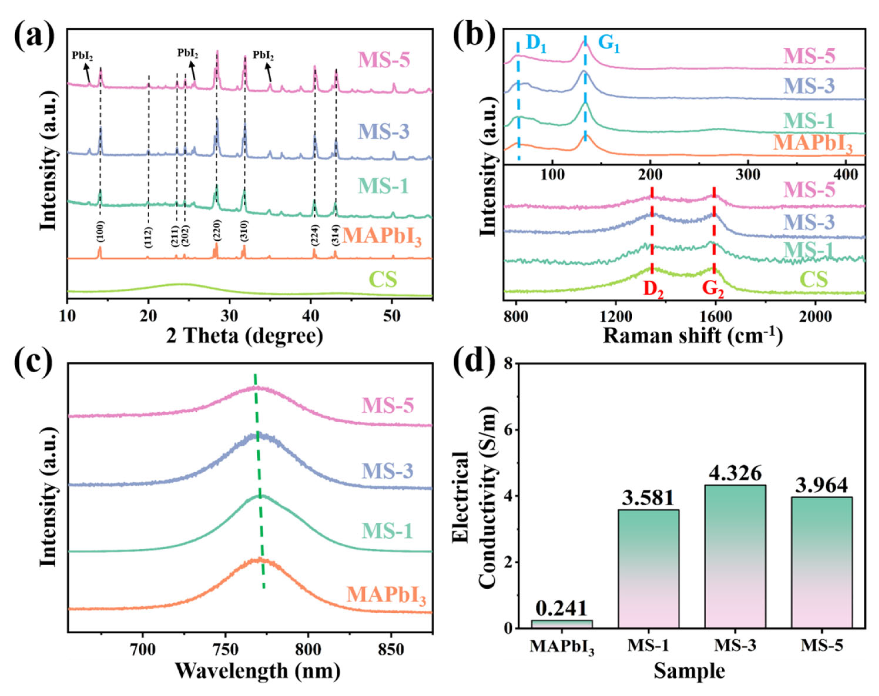
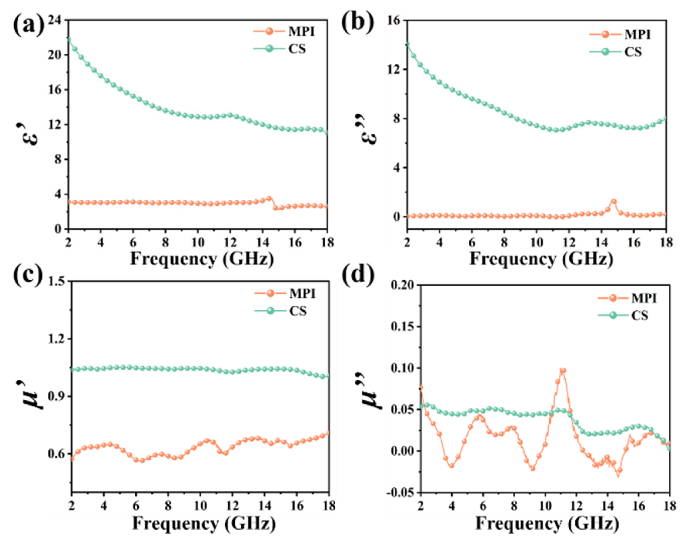
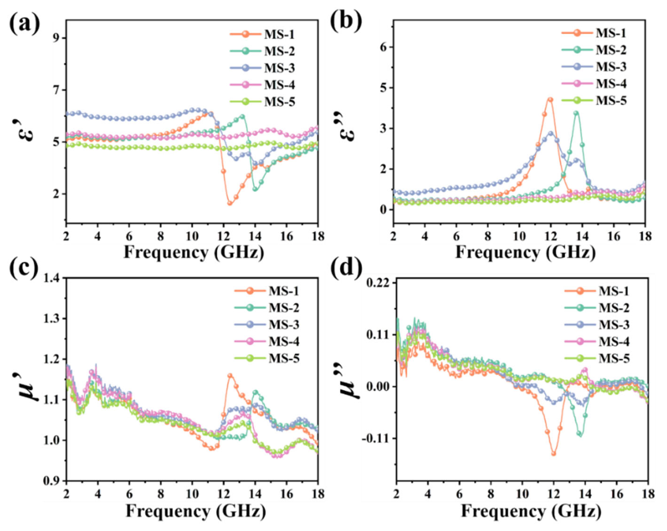
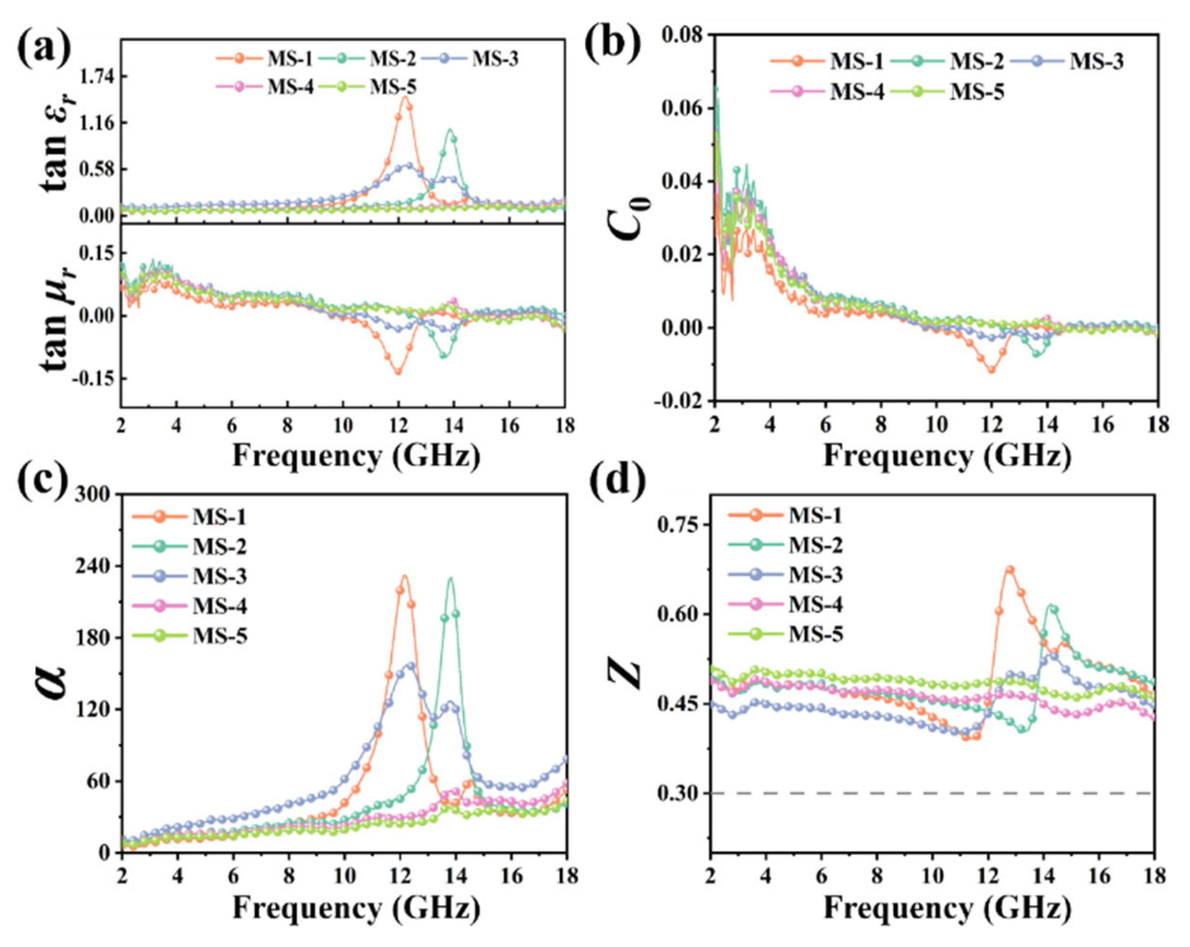
3. Results and Discussion

To investigate the physicochemical properties of MAPbI3/CS crystals, such as composition and lattice structure, we employed X-ray diffraction (XRD), Raman spectra, and Photoluminescence (PL) spectra (Figure 1). Figure 1a shows the XRD patterns of the MAPbI3/CS, MAPbI3, and CSs. It can be seen that the characteristic diffraction peaks in MAPbI3/CS (MS-1, MS-3, MS-5) are consistent with the main diffraction peaks of tetragonal-phase MAPbI3 crystals [29,30]. In addition, with the increased content of CSs, the intensity of the diffraction peak at 2θ = 12.6°, corresponding to PbI2, increased. The emergence of PbI2 indicates that introducing CSs could induce the partial decomposition of MAPbI3. In addition, it can be found that the characteristic diffraction peak of the CSs appears near 2θ = 24.1°, and the full wide of half maximum (FWHM) is relatively large, indicating that the CSs are partially graphitized.
Further, we contrasted the Raman spectra of the MAPbI3, CSs, and MAPbI3/CS (Figure 1b). By calculating the intensity ratio of the D1 and G1 peaks in Figure 1b, it is found that the ID1/IG1 values of MAPbI3, MS-1, MS-3, and MS-5 are 0.61, 0.71, 0.85, and 0.87, respectively. It can be found that with the increased content of CSs, the ID1/IG1 value of MAPbI3/CS increases. In the published works, a higher ID1/IG1 value indicates higher defect densities, which may originate from space charge polarization [31,32,33]. Thus, the CSs could impact the nucleation and crystallization process of MAPbI3 and induce defects. Although introducing CSs causes the partial decomposition of MAPbI3, the generated defects and vacancies may be conducive to electromagnetic wave absorption because the increased defects will cause increased space charge polarization, which may enhance the intensity of the polarization loss. Further, the D2 and G2 peaks correspond to the crystal vibration of carbon in CS at the symmetry point of A1g and the first-order scattering of E2g phonons by carbon atoms in the sp2 orbital, respectively [34]. As shown in Figure 1b, for each content of CSs, the ID2/IG2 values of MAPbI3/CS are 0.98, which indicates that CSs can stably exist.
According to Figure 1c, with the increased content of CSs in MAPbI3/CS, the PL peak position belonging to MAPbI3 (770 nm) showed a slight blue shift of about 5 nm, and the FWHM became larger. A larger FWHM indicates the partial decomposition of MPI crystals, which is consistent with the diffraction peak results of PbI2 in the XRD pattern. In addition, electrical conductivity is an important index for evaluating the conduction loss of the composites. According to Figure 1d, the conductivity of the MAPbI3 crystal is 0.2 S m−1. With the addition of CSs, the conductivity of MAPbI3/CS significantly improved, reaching the highest 4.3 S m−1 for MS-3. So, introducing CSs can improve the movement of free electrons between MAPbI3 crystals. However, the conductivity of MS-5 (3.9 S m−1) is lower than that of MS-3. The decreased conductivity can be explained by the fact that excessive CSs will lead to the decomposition of MAPbI3 crystals, reducing the entire conductivity of MAPbI3/CS.
The micro-morphology of MAPbI3/CS under different contents of CSs was characterized by SEM (Figure 2), in which MAPbI3 were bulk crystals [35] and CSs are typical spheres [36], with a radius of 0.5 μm, in all groups of components (MS-1, MS-3, MS-5). With the increased content of CSs, the size of the MAPbI3 crystals gradually decreased from larger than 5 μm (Figure 2a) to less than 1 μm (Figure 2c), which verified the above inference that the nucleation of the MAPbI3 crystals was affected by the CSs. At the same time, when the CS content is relatively low, CSs are sporadically distributed on the surface of the MAPbI3 crystals (Figure 2a). When the content of CSs increases, the CSs agglomerate (Figure 2c). In these scenarios of Figure 2a,c, the CSs cannot effectively improve the conductivity and interfacial polarization of the system. Only when the CS content is appropriate (Figure 2b) could CSs uniformly distribute on the surface or in the grain boundaries of MAPbI3, constructing a conductive network between MAPbI3 grains and maximizing the intensity of interfacial polarization in the system.
The complex permittivity and complex permeability of the MAPbI3 crystals and CSs were characterized, as shown in Figure 3. For the complex permittivity, the real part (ε′) and the imaginary part (ε″) of the CSs are much larger than the ε′ and ε″ of MAPbI3. Based on ε″ ≈ 1/πε0ρf [37], the conductivity of MAPbI3/CS mainly originates from the CSs. For the complex permeability, it can be seen that in the range of 2–18 GHz, the real part (μ′) and the imaginary part (μ″) of the CSs are larger than the μ′ and μ″ of MAPbI3. Furthermore, the μ′ and μ″ of the CSs are around 1.0 and 0.05, respectively. Therefore, it can be judged that MAPbI3/CS composites may be dominated by dielectric loss, not magnetic loss.
Then, the complex permittivity and complex permeability of MAPbI3/CS are shown in Figure 4. The ε′ and ε″ of all the MAPbI3/CS samples are higher than the MAPbI3 crystals, which is consistent with the results of the conductivity test. For the MS-1 and MS-2, the data of ε′ match the law of the resonant dispersion curve (Lorentz model) [38,39]. The peaks of ε″ appear at 12.0 GHz and 14.0 GHz, indicating that the electronic transition generates resonant absorption of electromagnetic waves. Therefore, the MS-1 and MS-2 samples may appear to have strong electromagnetic wave absorption at 12.0 GHz and 14.0 GHz, respectively. The ε′ and ε″ of MS-3 present multiple peaks within 10–16 GHz, indicating that the MS-3 may exhibit obvious polarization relaxation and resonance absorption, which may include (1) resonance absorption generated by electronic transitions, (2) dipole polarization of MA+ and space charge polarization caused by defects, and (3) turning-direction polarization of an intrinsic dipole moment [8]. Therefore, it can be predicted that the MS-3 may appear to have strong wave-absorption capabilities within 10–16 GHz. The μ′ and μ″ of MAPbI3/CS are low, indicating that MAPbI3/CS has poor magnetic loss to electromagnetic waves. The peaks of μ′ and μ″ in MS-1 and MS-2 may originate from eddy current loss, natural resonance, and exchange resonance. Further analysis of the coefficient of eddy current loss is necessary.
To evaluate the dissipation ability of the material to the incident electromagnetic wave, we calculate the dielectric loss tangent and magnetic loss tangent [40]. The tanδε and tanδµ of MAPbI3/CS are shown in Figure 5a. Within 10–16 GHz, the peak positions of tanδε and tanδµ of MS-1, MS-2, and MS-3 are consistent with ε″ and μ″, respectively. Then, we calculate the eddy current loss coefficient (C0) of MAPbI3/CS at each content of CS [41]:
C 0 = μ μ f
As shown in Figure 5b, within 2–10 GHz, the values of C0 fluctuate significantly within the electromagnetic frequency, indicating that eddy current loss does not exist [41]. Within 14.5–18.0 GHz, the value of C0 is close to 0, indicating obvious eddy current loss. However, the tanδµ of MAPbI3/CS is close to 0 within 14.5–18.0 GHz. So, the magnetic loss intensity of MAPbI3/CS is negligible, and the electromagnetic wave absorption is dominated by dielectric loss. This slight magnetic loss may originate from the weak natural lattice resonance.
Furthermore, the attenuation constant (α) is calculated according to the following Formula [42]:
α = 2 π f c × μ ε     μ ε   +   μ ε     μ ε 2   +   μ ε   +   μ ε 2
where c is the speed of light in vacuum. Z can be calculated according to the following Formulas [43]:
Z = Z r / Z 0
Z r = Z 0 μ r / ε r
where Zr is the material’s intrinsic impedance and Z0 is the free space impedance. As shown in Figure 5c, the α of MS-1, MS-2, and MS-3 is larger than 100 within 11.0–15.0 GHz, although MS-1 and MS-2 exhibit a jitter at 12 GHz and 14 GHz, in comparison with MS-3. However, MS-3 shows a larger α within 2–18 GHz, except for the peaks at 12 GHz and 14 GHz. As shown in Figure 5d, all the intrinsic impedance ratios of MAPbI3/CS at each content of CS exceed 0.3 within 2–18 GHz. Therefore, all the MAPbI3/CS composites have excellent transmittance to electromagnetic waves [44], and the component of CS in MS-3 is optimum. Meanwhile, we investigate the Debye relaxation properties of MAPbI3/CS, which can be found in the Supplementary Materials (Figure S1).
The reflection loss (RL) of MAPbI3/CS in the range of 2–18 GHz can be calculated according to the following Formulas [25,45]:
Z in = Z 0 μ r ε r tan h j 2 π fd c μ r ε r
RL dB = 20 lg Z in Z 0 Z in + Z 0
where Zin is the input impedance. Figure 6 exhibits RL values for MAPbI3, CS, and MAPbI3/CS. For MS-3, the effective electromagnetic wave absorption bandwidth (EAB) reaches 4 GHz (10.24–14.24 GHz), with a maximum reflection loss of −54 dB at 12 GHz and a thickness of 2.9 mm. In contrast, MS-1 and MS-2 only exhibit reflection loss around −42 dB at 12 GHz and 14 GHz with just 1 GHz of EAB. For MS-4 and MS-5, neither of the RLs reach −10 dB within 2–18 GHz. All the variation laws of reflection loss of MS under each CS ratio are consistent with the corresponding electromagnetic parameters, attenuation loss coefficient, and intrinsic impedance ratio in Figure 4 and Figure 5. For MAPbI3/CS, the wave dissipation contains polarization loss from MAPbI3 and conduction loss from CSs. For MAPbI3, the MA+ dipole, crystal defects, and crystal interface are the origins of the polarization loss. Combining the above data, we can demonstrate that induced CSs can enhance the intensity of the polarization loss and conduction loss. However, excessive CSs can cause the severe decomposition of MAPbI3 crystals, weakening the dipole and interfacial polarization loss.
According to the reflection loss performance of MAPbI3/CS in Figure 6, we extracted the EAB and its corresponding thickness, the maximum reflection loss intensity, and the corresponding thickness of MS-1, MS-2, and MS-3, as shown in Figure 7a,b. The MS-3 has the highest EAB and maximum reflection loss intensity, which are the optimum performance under 40 wt% addition. In addition, the maximum reflection loss intensity, normalized input impedance, and matched thickness correlations of the MS-1, MS-2, and MS-3 samples are shown in Figure 7c–e, where the normalized input impedance is calculated according to Formula (7) and the matched thickness is calculated according to the following Formula [37]:
t m = n λ 4 = nc 4 f m μ r ε r ,   n = 1 , 3 , 5 ,
When the normalized input impedance values of the MS-1, MS-2, and MS-3 samples are close to 1.0, the reflection loss intensity of the samples reaches its maximum value. To summarize, MAPbI3/CS is a dielectric-loss-dominated absorbing material in which MAPbI3 crystals contribute to the core of dipole and space charge polarization. CSs enhance the interfacial polarization of the system and improve the movement of free electrons in MAPbI3 crystals due to their high surface area and high conductivity.

4. Conclusions

A MAPbI3-dominated MAPbI3/CS composite with a simple synthesis method and improved electromagnetic wave absorption ability was successfully developed. MS composites were characterized and analyzed by various means, and the electromagnetic wave absorption properties were deeply studied. We explored the optimal ratio of CS components in MAPbI3 and analyzed the wave-absorption mechanism. When the mass ratio of MAPbI3:CS is 12:1, the composite absorber reaches a high absorption strength of −54 dB at 12 GHz (40 wt%) and an effective absorption bandwidth of 4 GHz, revealing a promising application foreground of perovskite materials in the field of electromagnetic wave absorption. Moreover, this work proves the possibility of preparing electromagnetic wave-absorbing materials by combining perovskite-based material with multi-dimensional carbon materials. Also, it reveals a reliable strategy for achieving higher electromagnetic wave absorbing performance through improving the interfacial polarization and conductivity of the composite absorber.

Supplementary Materials

The following supporting information can be downloaded at https://www.mdpi.com/article/10.3390/nano14191566/s1, Figure S1: Cole-Cole diagram of MS-1 (a), MS-2 (b), MS-3 (c), MS-4 (d), and MS-5 (e), and the number of Cole-Cole semicircles in the MAPbI3/CS composites (f); Figure S2: Impedance matching performance of MS-1 (a), MS-2 (b), MS-3 (c), MS-4 (d), and MS-5 (e). Reference [46] is included in the Supplementary Materials.

Author Contributions

Conceptualization, Z.Z. and Y.Y.; methodology, Y.D. (Yantao Duan), J.W., S.F. and W.Z.; software, W.Z.; validation, Z.X. and W.Z.; formal analysis, Y.D. (Yantao Duan); investigation, Z.Z. and J.W.; resources, W.Z.; writing—original draft preparation, X.L.; writing—review and editing, Z.Z.; visualization, W.Z. and Y.D. (Yinsuo Dai). All authors have read and agreed to the published version of the manuscript.

Funding

This work was supported by the Nature Science Foundation of Jiangsu Province (No. BK20221055, No. BK20241602), the Chinese Postdoctoral Science Fund (No. 2020M683756), the State Key Laboratory of Disaster Prevention & Mitigation of Explosion & Impact (No. LGD-SKL-202203), and the Army Engineering University Youth Independent Innovation Fund (No. KYFYJKQTZQ23006).

Data Availability Statement

The data that support the findings of this study are available from the corresponding authors upon reasonable request.

Conflicts of Interest

The authors declare no conflicts of interest.

References

  1. Zeng, X.; Zhao, C.; Jiang, X.; Yu, R.; Che, R. Functional Tailoring of Multi-dimensional Pure MXene Nanostructures for Significantly Accelerated electromagnetic Wave Absorption. Small 2023, 19, 2303393. [Google Scholar] [CrossRef] [PubMed]
  2. Wang, Y.; Yao, L.; Zheng, Q.; Cao, M.-S. Graphene-wrapped multiloculated nickel ferrite: A highly efficient electromagnetic attenuation material for microwave absorbing and green shielding. Nano Res. 2022, 15, 6751–6760. [Google Scholar] [CrossRef]
  3. Cao, M.; Han, C.; Wang, X.; Zhang, M.; Zhang, Y.; Shu, J.; Yang, H.; Fang, X.; Yuan, J. Graphene nanohybrids: Excellent electromagnetic properties for the absorbing and shielding of electromagnetic waves. J. Mater. Chem. C 2018, 6, 4586–4602. [Google Scholar] [CrossRef]
  4. Wang, F.; Gu, W.; Chen, J.; Wu, Y.; Zhou, M.; Tang, S.; Cao, X.; Zhang, P.; Ji, G. The point defect and electronic structure of K doped LaCo0.9Fe0.1O3 perovskite with enhanced microwave absorbing ability. Nano Res. 2021, 15, 3720–3728. [Google Scholar] [CrossRef]
  5. Miao, P.; Yang, J.; Liu, Y.; Xie, H.; Chen, K.-J.; Kong, J. Emerging Perovskite Electromagnetic Wave Absorbers from Bi-Metal-Organic Frameworks. Cryst. Growth Des. 2020, 20, 4818–4826. [Google Scholar] [CrossRef]
  6. Miao, P.; Qu, N.; Chen, W.; Wang, T.; Zhao, W.; Kong, J. A two-dimensional semiconductive Cu-S metal-organic framework for broadband microwave absorption. Chem. Eng. J. 2023, 454, 140445. [Google Scholar] [CrossRef]
  7. Zhang, Z.; Yao, Y.; Zhang, J.; Ma, Y.; Xu, P.; Zhang, P.; Yang, Z.; Zhou, W. Two-dimensional (PEA)2PbBr4 perovskite modified with conductive network for high-performance electromagnetic wave absorber. Mater. Lett. 2022, 326, 132926. [Google Scholar] [CrossRef]
  8. Zhang, Z.; Xiong, Z.; Yao, Y.; Wang, D.; Yang, Z.; Zhang, P.; Zhao, Q.; Zhou, W. Constructing Conductive Network in Hybrid Perovskite for a Highly Efficient Microwave Absorption System. Adv. Funct. Mater. 2022, 32, 2206053. [Google Scholar] [CrossRef]
  9. Zhang, Z.; Xiong, Z.; Yao, Y.; Shi, X.; Zhang, P.; Yang, Z.; Zhao, Q.; Zhou, W. Inorganic Halide Perovskite Electromagnetic Wave Absorption System with Ultra-Wide Absorption Bandwidth and High Thermal-Stability. Adv. Electron. Mater. 2022, 9, 2201179. [Google Scholar] [CrossRef]
  10. Qin, F.; Chen, J.; Liu, J.; Liu, L.; Tang, C.; Tang, B.; Li, G.; Zeng, L.; Li, H.; Yi, Z. Design of high efficiency perovskite solar cells based on inorganic and organic undoped double hole layer. Sol. Energy 2023, 262, 111796. [Google Scholar] [CrossRef]
  11. Guo, H.; Yang, J.; Pu, B.; Chen, H.; Li, Y.; Wang, Z.; Niu, X. Excellent microwave absorption of lead halide perovskites with high stability. J. Mater. Chem. C 2018, 6, 4201–4207. [Google Scholar] [CrossRef]
  12. Zhao, B.; Li, Y.; Wang, Z.; Ding, J.; Zhang, R.; Che, R. Galvanic Replacement Reaction Involving Core-Shell Magnetic Chains and Orientation-Tunable Microwave Absorption Properties. Small 2020, 16, 2003502. [Google Scholar] [CrossRef] [PubMed]
  13. Wu, Z.; Pei, K.; Xing, L.; Yu, X.; You, W.; Che, R. Enhanced Microwave Absorption Performance from Magnetic Coupling of Magnetic Nanoparticles Suspended within Hierarchically Tubular Composite. Adv. Funct. Mater. 2019, 29, 1901448. [Google Scholar] [CrossRef]
  14. Xu, J.; Wang, Z.; Ge, C.; Qi, X.; Bao, Q.; Liu, C. Constructing MXene-based mixed-dimensional structure with multiple interfaces to optimize dielectric-magnetic synergistic effect for effective electromagnetic wave absorption. J. Colloid Interf. Sci. 2024, 667, 529–539. [Google Scholar] [CrossRef] [PubMed]
  15. Liu, J.; Zhang, L.; Wu, H.; Zang, D. Boosted electromagnetic wave absorption performance from vacancies, defects and interfaces engineering in Co(OH)F/Zn0.76Co0.24S/Co3S4 composite. Chem. Eng. J. 2021, 411, 128601. [Google Scholar] [CrossRef]
  16. Zhao, B.; Yan, Z.; Liu, L.; Zhang, Y.; Guan, L.; Guo, X.; Li, R.; Che, R.; Zhang, R. A Liquid-Metal-Assisted Competitive Galvanic Reaction Strategy Toward Indium/Oxide Core-Shell Nanoparticles with Enhanced Microwave Absorption. Adv. Funct. Mater. 2024, 34, 2314008. [Google Scholar] [CrossRef]
  17. Pan, Y.; Lan, D.; Jia, Z.; Feng, A.; Wu, G.; Yin, P. Multi-mode tunable electromagnetic wave absorber based on hollow nano-cage structure and self-anticorrosion performance. Adv. Compos. Hybrid Mater. 2024, 7, 40. [Google Scholar] [CrossRef]
  18. Zhong, X.; He, M.; Zhang, C.; Guo, Y.; Hu, J.; Gu, J. Heterostructured BN@Co-C@C Endowing Polyester Composites Excellent Thermal Conductivity and Microwave Absorption at C Band. Adv. Funct. Mater. 2024, 34, 231355. [Google Scholar] [CrossRef]
  19. Zhang, C.; Chen, G.; Zhang, R.; Wu, Z.; Xu, C.; Man, H.; Che, R. Charge modulation of CNTs-based conductive network for oxygen reduction reaction and microwave absorption. Carbon 2021, 178, 310–319. [Google Scholar] [CrossRef]
  20. Hu, Q.; Yang, R.; Mo, Z.; Lu, D.; Yang, L.; He, Z.; Zhu, H.; Tang, Z.; Gui, X. Nitrogen-doped and Fe-filled CNTs/NiCo2O4 porous sponge with tunable microwave absorption performance. Carbon 2019, 153, 737–744. [Google Scholar] [CrossRef]
  21. Gao, Z.; Zhao, Z.; Lan, D.; Kou, K.; Zhang, J.; Wu, H. Accessory ligand strategies for hexacyanometallate networks deriving perovskite polycrystalline electromagnetic absorbents. J. Mater. Sci. Technol. 2021, 82, 69–79. [Google Scholar] [CrossRef]
  22. Wang, K.; Zhang, S.; Chu, W.; Li, H.; Chen, Y.; Chen, B.; Chen, B.; Liu, H. Tailoring conductive network nanostructures of ZIF-derived cobalt-decorated N-doped graphene/carbon nanotubes for microwave absorption applications. J. Colloid Interf. Sci. 2021, 591, 463–473. [Google Scholar] [CrossRef] [PubMed]
  23. Deshmukh, A.A.; Mhlanga, S.D.; Coville, N.J. Carbon spheres. Mater. Sci. Eng. R Rep. 2010, 70, 1–28. [Google Scholar] [CrossRef]
  24. Ding, S.; Zhang, C.; Qu, X.; Liu, J.; Lu, Y.; Yang, Z. Porous carbon and carbon composite hollow spheres. Colloid Polym. Sci. 2008, 286, 1093–1096. [Google Scholar] [CrossRef]
  25. Cheng, Y.; Li, Z.; Li, Y.; Dai, S.; Ji, G.; Zhao, H.; Cao, J.; Du, Y. Rationally regulating complex dielectric parameters of mesoporous carbon hollow spheres to carry out efficient microwave absorption. Carbon 2018, 127, 643–652. [Google Scholar] [CrossRef]
  26. Wang, Y.; Han, X.; Xu, P.; Liu, D.; Cui, L.; Zhao, H.; Du, Y. Synthesis of pomegranate-like Mo2C@C nanospheres for highly efficient microwave absorption. Chem. Eng. J. 2019, 372, 312–320. [Google Scholar] [CrossRef]
  27. Weir, W.B. Automatic Measurement of Complex Dielectric Constant and Permeability at Microwave Frequencies. Proc. IEEE 1974, 62, 33–36. [Google Scholar] [CrossRef]
  28. Nicolson, A.M.; Ross, G.F. Measurement of the Intrinsic Properties of materials by Time-Domain Techniques. IEEE Trans. Instrum. Meas. 1970, 19, 377–382. [Google Scholar] [CrossRef]
  29. Liu, Y.; Yang, Z.; Cui, D.; Ren, X.; Sun, J.; Liu, X.; Zhang, J.; Wei, Q.; Fan, H.; Yu, F.; et al. Two-Inch-Sized Perovskite CH3NH3PbX3 (X = Cl, Br, I) Crystals: Growth and Characterization. Adv. Mater. 2015, 27, 5176–5183. [Google Scholar] [CrossRef]
  30. Zhang, C.; Mu, C.; Xiang, J.; Wang, B.; Wen, F.; Song, J.; Wang, C.; Liu, Z. Microwave absorption characteristics of CH3NH3PbI3 perovskite/carbon nanotube composites. J. Mater. Sci. 2017, 52, 13023–13032. [Google Scholar] [CrossRef]
  31. Chang, S.; Chen, C.; Chen, L.; Tien, C.; Cheng, H.; Huang, W.; Lin, H.; Chen, S.; Wu, G. Unraveling the multifunctional capabilities of PCBM thin films in inverted-type CH3NH3PbI3 based photovoltaics. Sol. Energy Mater. Sol. Cells 2017, 169, 40–46. [Google Scholar] [CrossRef]
  32. Chen, X.; Xu, Y.; Wang, Z.; Wu, R.; Cheng, H.; Chui, H. Characterization of a CH3NH3PbI3 perovskite microwire by Raman spectroscopy. J. Raman Spectrosc. 2022, 53, 288–296. [Google Scholar] [CrossRef]
  33. Pérez-Osorio, M.A.; Milot, R.L.; Filip, M.R.; Patel, J.B.; Herz, L.M.; Johnston, M.B.; Giustino, F. Vibrational Properties of the Organic-Inorganic Halide Perovskite CH3NH3PbI3 from Theory and Experiment: Factor Group Analysis, First-Principles Calculations, and Low-Temperature Infrared Spectra. J. Phys. Chem. C 2015, 119, 25703–25718. [Google Scholar] [CrossRef]
  34. Ray, S.C.; Tetana, Z.N.; Erasmus, R.; Mathur, A.; Coville, N.J. Carbon spheres for energy applications: Raman and X-ray photoemission spectroscopy studies. Int. J. Energy Res. 2014, 38, 444–451. [Google Scholar] [CrossRef]
  35. Jia, X.; Hu, Z.; Zhu, Y.; Weng, T.; Wang, J.; Zhang, J.; Zhu, Y. Facile synthesis of organic-inorganic hybrid perovskite CH3NH3PbI3 microcrystals. J. Alloys Compd. 2017, 725, 270–274. [Google Scholar] [CrossRef]
  36. Wang, P.; Wei, J.; Huang, B.; Qin, X.; Yao, S.; Zhang, Q.; Wang, Z.; Xu, G.; Jing, X. Synthesis and characterization of carbon spheres prepared by chemical vapour deposition. Mater. Lett. 2007, 61, 4854–4856. [Google Scholar] [CrossRef]
  37. Quan, B.; Liang, X.; Xu, G.; Cheng, Y.; Zhang, Y.; Liu, W.; Ji, G.; Du, Y. A permittivity regulating strategy to achieve high performance electromagnetic wave absorbers with compatibility of impedance matching and energy conservation. New J. Chem. 2017, 41, 1259–1266. [Google Scholar] [CrossRef]
  38. Wang, N.; You, K.; Mohanavel, V.; Mehrez, S.; Alamri, S.; Nag, K.; Mahariq, I. Comprehensive study of electromagnetic wave absaorption properties of GdMnO3-MoSe2 hybrid composites. Ceram. Int. 2023, 49, 9191–9202. [Google Scholar] [CrossRef]
  39. Jiang, C.; Liu, D.; Wang, R.; Wang, M.; Cao, M.; Ye, W.; Long, X.; Yuan, G. Drude-Lorentz resonance absorption in quasi-2D NiFe hydrotalcite/less layer graphite composites. Appl. Phys. A Mater. Sci. Process. 2023, 129, 5. [Google Scholar] [CrossRef]
  40. Zhao, B.; Shao, G.; Fan, B.; Zhao, W.; Zhang, R. Investigation of the electromagnetic absorption properties of Ni@TiO2 and Ni@SiO2 composite microspheres with core-shell structure. Phys. Chem. Chem. Phys. 2015, 17, 2531–2539. [Google Scholar] [CrossRef] [PubMed]
  41. Zhao, B.; Shao, G.; Fan, B.; Zhao, W.; Xie, Y.; Zhang, R. Facile preparation and enhanced microwave absorption properties of core-shell composite spheres composited of Ni cores and TiO2 shells. Phys. Chem. Chem. Phys. 2015, 17, 8802–8810. [Google Scholar] [CrossRef]
  42. Xie, A.; Sun, M.; Zhang, K.; Jiang, W.; Wu, F.; He, M. In situ growth of MoS2 nanosheets on reduced graphene oxide (RGO) surfaces: Interfacial enhancement of absorbing performance against electromagnetic pollution. Phys. Chem. Chem. Phys. 2016, 18, 24931–24936. [Google Scholar] [CrossRef] [PubMed]
  43. Sun, X.; Yuan, X.; Li, X.; Li, L.; Song, Q.; Lv, X.; Gu, G.; Sui, M. Hollow cube-like CuS derived from Cu2O crystals for the highly efficient elimination of electromagnetic pollution. New J. Chem. 2018, 42, 6735–6741. [Google Scholar] [CrossRef]
  44. Moitra, D.; Dhole, S.; Ghosh, B.K.; Chandel, M.; Jani, R.K.; Patra, M.K.; Vadera, S.R.; Ghosh, N.N. Synthesis and microwave absorption properties of BiFeO3 nanowire-RGO nanocomposite and first-principles calculations for insight of electromagnetic properties and electronic structures. J. Phys. Chem. C 2017, 121, 21290. [Google Scholar] [CrossRef]
  45. Qin, M.; Zhang, L.; Wu, H. Dielectric Loss Mechanism in Electromagnetic Wave Absorbing Materials. Adv. Sci. 2022, 9, 2105553. [Google Scholar] [CrossRef]
  46. Song, L.; Duan, Y.; Liu, J.; Pang, H. Transformation between nanosheets and nanowires structure in MnO2 upon providing Co2+ ions and applications for microwave absorption. Nano Res. 2020, 13, 95–104. [Google Scholar] [CrossRef]
Figure 1. The XRD spectra (a), Raman spectra (b), PL spectra (c), and conductivity plot (d) of the MAPbI3/CS composite.
Nanomaterials 14 01566 g001
Figure 2. SEM photograph of MS-1 (a), MS-3 (b), MS-5 (c), and CS (d).
Nanomaterials 14 01566 g002
Figure 3. Real part of complex permittivity ε′ (a), imaginary part of complex permittivity ε″ (b), real part of complex permeability μ′ (c), and imaginary part of complex permeability μ″ (d) of MAPbI3 and CSs within 2–18 GHz.
Nanomaterials 14 01566 g003
Figure 4. Real part of complex dielectric (ε′) (a), imaginary part of complex dielectric (ε″) (b), real part of complex permeability (μ′) (c), and imaginary part of complex permeability (μ″) (d) of MAPbI3/CS composites within 2–18 GHz.
Nanomaterials 14 01566 g004
Figure 5. Dielectric loss tangent and magnetic loss tangent (a), eddy current loss constant (b), attenuation loss coefficient (c), and intrinsic impedance ratio (d) of MAPbI3/CS composites.
Nanomaterials 14 01566 g005
Figure 6. Schematic diagram of three-dimensional reflection loss performance of MS-1 (a), MS-2 (b), MS-3 (c), MS-4 (d), and MS-5 (e), and two-dimensional reflection loss performance of MS-3 (f).
Nanomaterials 14 01566 g006
Figure 7. EAB properties of MAPbI3/CS and corresponding thicknesses (a), maximum reflection loss intensity of MAPbI3/CS and corresponding thicknesses (b), maximum reflection loss intensity of MAPbI3/CS (c), normalized input impedance of MAPbI3/CS (d), and matched thickness correlation comparison chart (e).
Nanomaterials 14 01566 g007
Disclaimer/Publisher’s Note: The statements, opinions and data contained in all publications are solely those of the individual author(s) and contributor(s) and not of MDPI and/or the editor(s). MDPI and/or the editor(s) disclaim responsibility for any injury to people or property resulting from any ideas, methods, instructions or products referred to in the content.

