Article

ITO-Based Electrically Tunable Metasurface for Active Control of Light Transmission

1
Key Laboratory of Light Field Manipulation and Information Acquisition, Ministry of Industry and Information Technology, Xi’an 710129, China
2
Shaanxi Key Laboratory of Optical Information Technology, School of Physical Science and Technology, Northwestern Polytechnical University, Xi’an 710129, China
*
Authors to whom correspondence should be addressed.
Nanomaterials 2024, 14(19), 1606; https://doi.org/10.3390/nano14191606
Submission received: 4 September 2024 / Revised: 24 September 2024 / Accepted: 4 October 2024 / Published: 5 October 2024
(This article belongs to the Special Issue Physical Properties of Semiconductor Nanostructures and Devices)

Abstract

:
In recent years, the rapid development of dynamically tunable metasurfaces has provided a new avenue for flexible control of optical properties. This paper introduces a transmission-type electrically tunable metasurface, employing a series of subwavelength-scale silicon (Si) nanoring structures with an intermediate layer of Al2O3-ITO-Al2O3. This design allows the metasurface to induce strong Mie resonance when transverse electric (TE) waves are normally incident. When a bias voltage is applied, the interaction between light and matter is enhanced due to the formation of an electron accumulation layer at the ITO-Al2O3 interface, thereby altering the resonance characteristics of the metasurface. This design not only avoids the absorption loss of metal nanostructures and has a large modulation depth, but also shows compatibility with complementary metal oxide semiconductor (CMOS) technology.

1. Introduction

Metasurfaces are two-dimensional nanostructured surfaces that enable versatile wavefront control of light, and play a significant role in controlling the amplitude, phase, and polarization of reflected/transmitted light [1,2,3,4,5]. In addition to being significantly thinner than conventional optical elements, metasurfaces exhibit heightened sensitivity to variations in the dielectric environment, particularly to those due to resonances [6]. This sensitivity is further enhanced by employing field-concentrating designs. As a result, these metasurfaces allow for dynamic tuning, which can be achieved through various methods, such as electrical, optical, mechanical, and phase-change controls. One approach to facilitating this tunability is by incorporating plasmonic metasurfaces with active materials. By appropriately designing metasurfaces and selecting suitable tunable materials, dynamic control over physical parameters such as the phase and amplitude of light can be achieved [7]. Currently, commonly used tunable materials include liquid crystals [8,9,10], conductive oxide materials [11], two-dimensional materials [12], and phase-change materials [13]. Indium tin oxide (ITO) has garnered significant attention as an active electro-optical material, primarily due to its substantial refractive index variation and broad tuning capability; it has been widely used in the active control of dielectric singularities [14], in broadband infrared metamaterial absorbers [15], and so on. This material also features an epsilon-near-zero (ENZ) frequency range, where its permittivity transitions from positive to negative. Additionally, ITO exhibits a rapid response time at near-infrared (NIR) wavelengths, notably including the 1.55 μm wavelength used in telecommunications. Huang et al. [16] experimentally demonstrated a gate-tunable metasurface capable of dynamically controlling the phase and amplitude of the reflected plane wave through electrical modulation. This tunability is achieved via field-effect modulation of the complex refractive index of conducting oxide layers, which are integrated into metasurface antenna elements arranged in a reflect-array configuration. By applying a 2.5 V gate bias, a phase shift of π and an approximately 30% variation in reflectance are realized. Park et al. [17] introduced an all-solid-state, electrically tunable metasurface array capable of generating a specific phase or performing a continuous phase sweep from 0 to 360° at a frequency of approximately 5.4 MHz, while simultaneously modulating the amplitude. A key innovation in their design is the incorporation of two independent control parameters—top and bottom gate voltages—within each nanoresonator. This configuration allows for precise and independent adjustment of the real and imaginary components of the reflection coefficient, enhancing the metasurface’s tunability and functionality. These metasurfaces successfully achieve dynamic regulation of the beam; however, most metasurfaces based on dynamically tunable structures are primarily of the metal–insulator–metal (MIM) type, with less amplitude modulation or lower modulation depth in the transmission spectrum.
In this paper, we present an ITO-integrated all-dielectric metasurface for amplitude modulation in the transmission mode. A series of subwavelength-scale nanorings with carefully chosen inner and outer radii and periodicity are employed. This structural design enables the metasurface to induce strong Mie resonances and leads to field confinement in the ITO layer with TE-polarized light. To evaluate the optical and electrical performance of the metasurface, we calculated the voltage-dependent carrier distribution profiles for ITO and silicon (Si) using the Poisson equation and the electron–hole drift-diffusion equation. These profiles are then used as input for optical simulations to accurately determine the transmission responses under an applied bias voltage. Further investigation reveals significant variations in the modulation depth of the transmission spectrum at different voltages by altering the inner diameter of the nanorings. This design not only achieves significant breakthroughs in performance but also provides new insights and methods for studying electrically tunable metasurfaces.

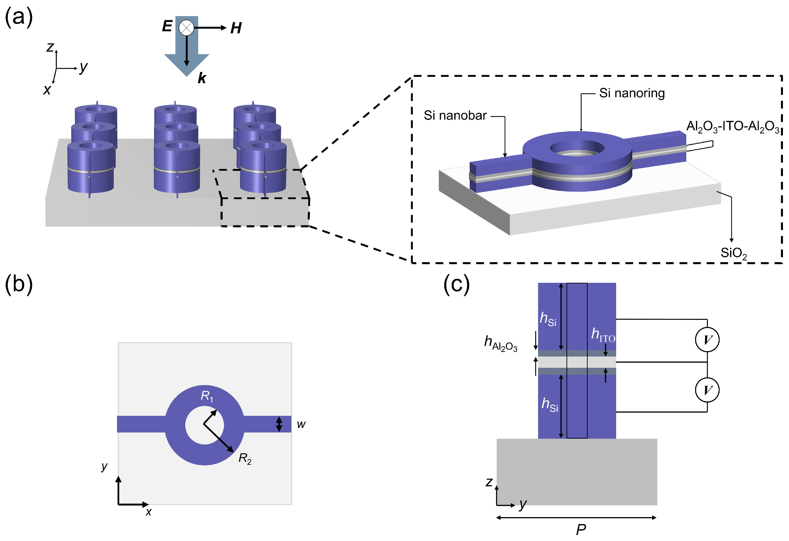
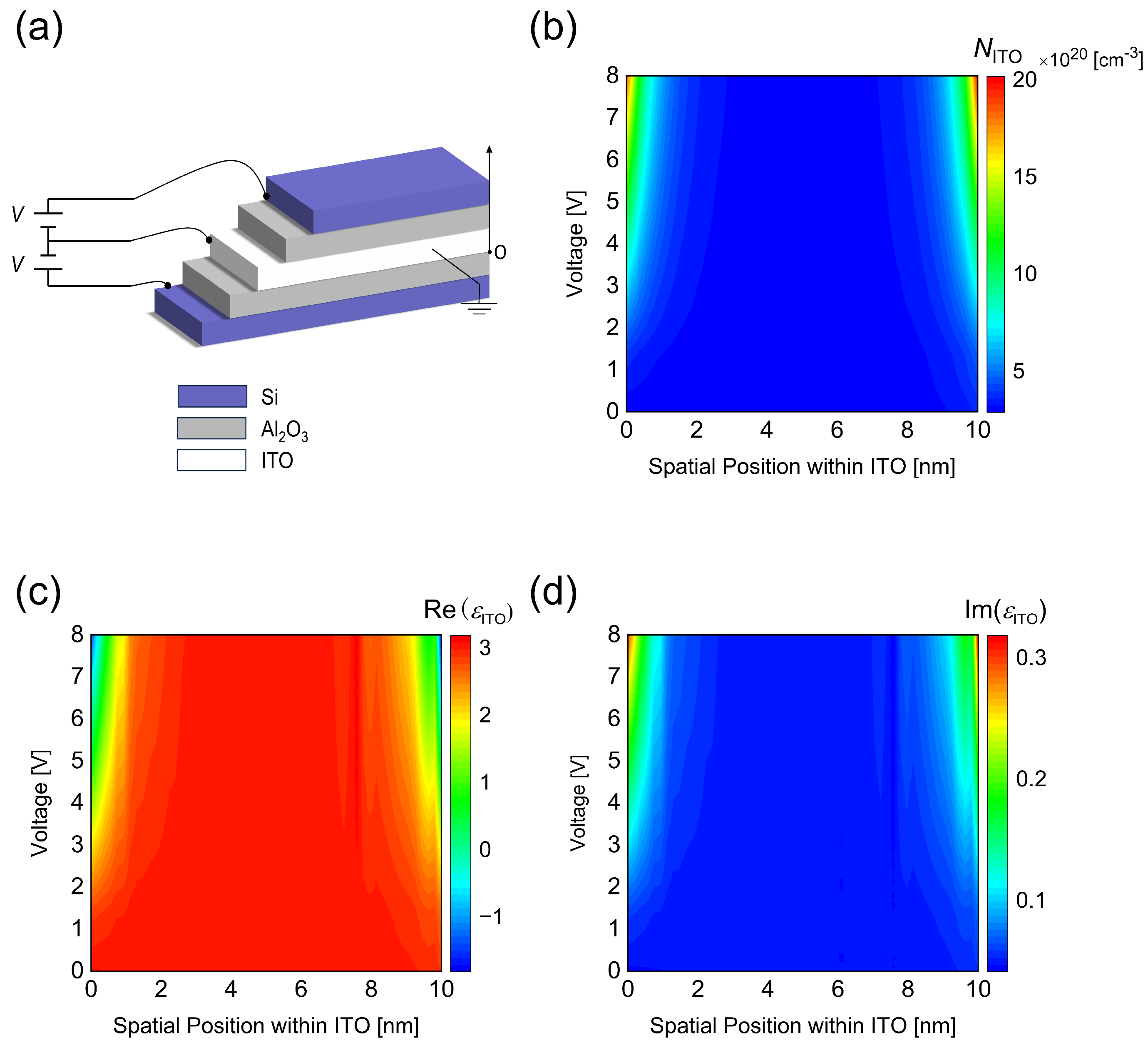
2. Materials and Methods
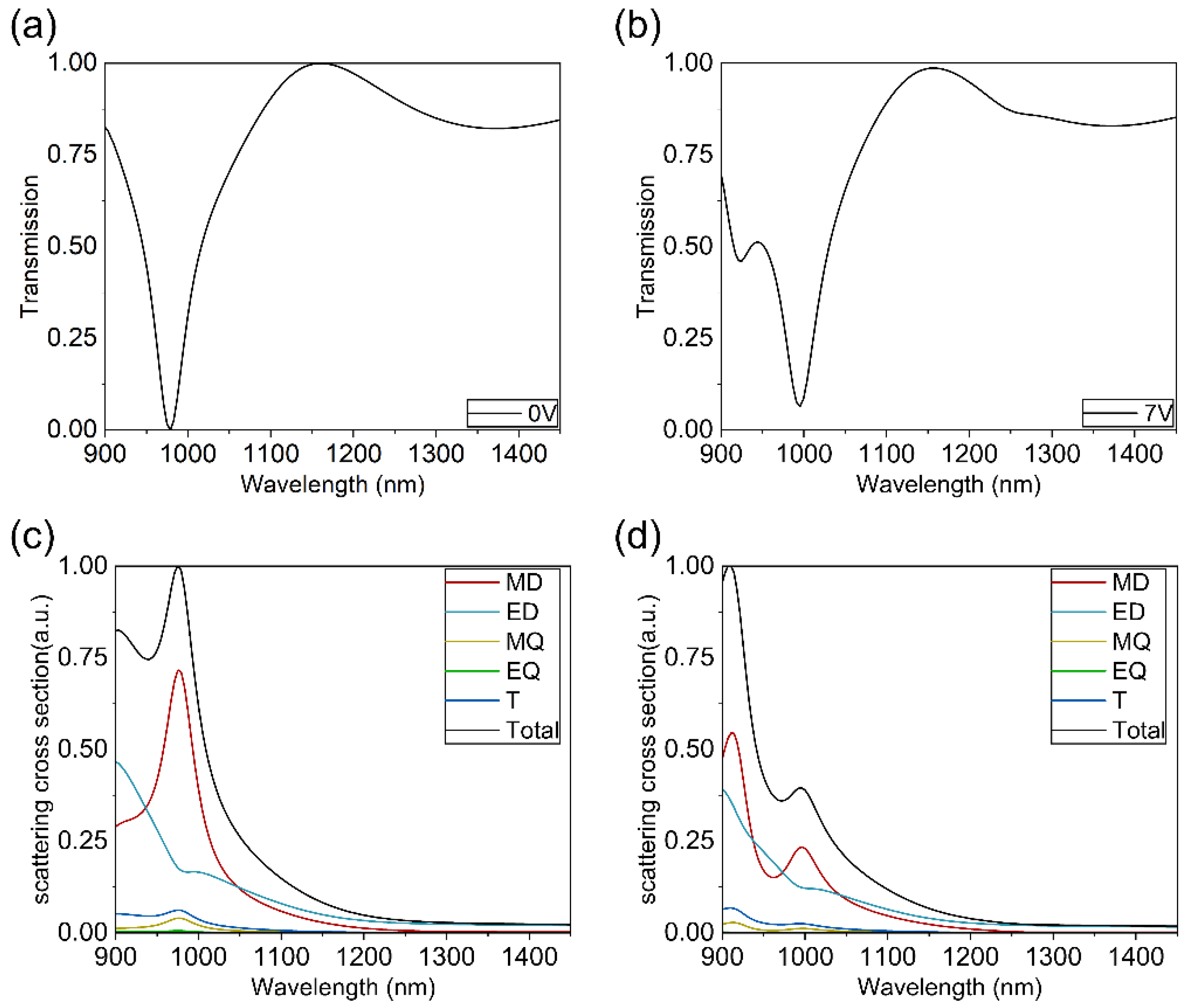
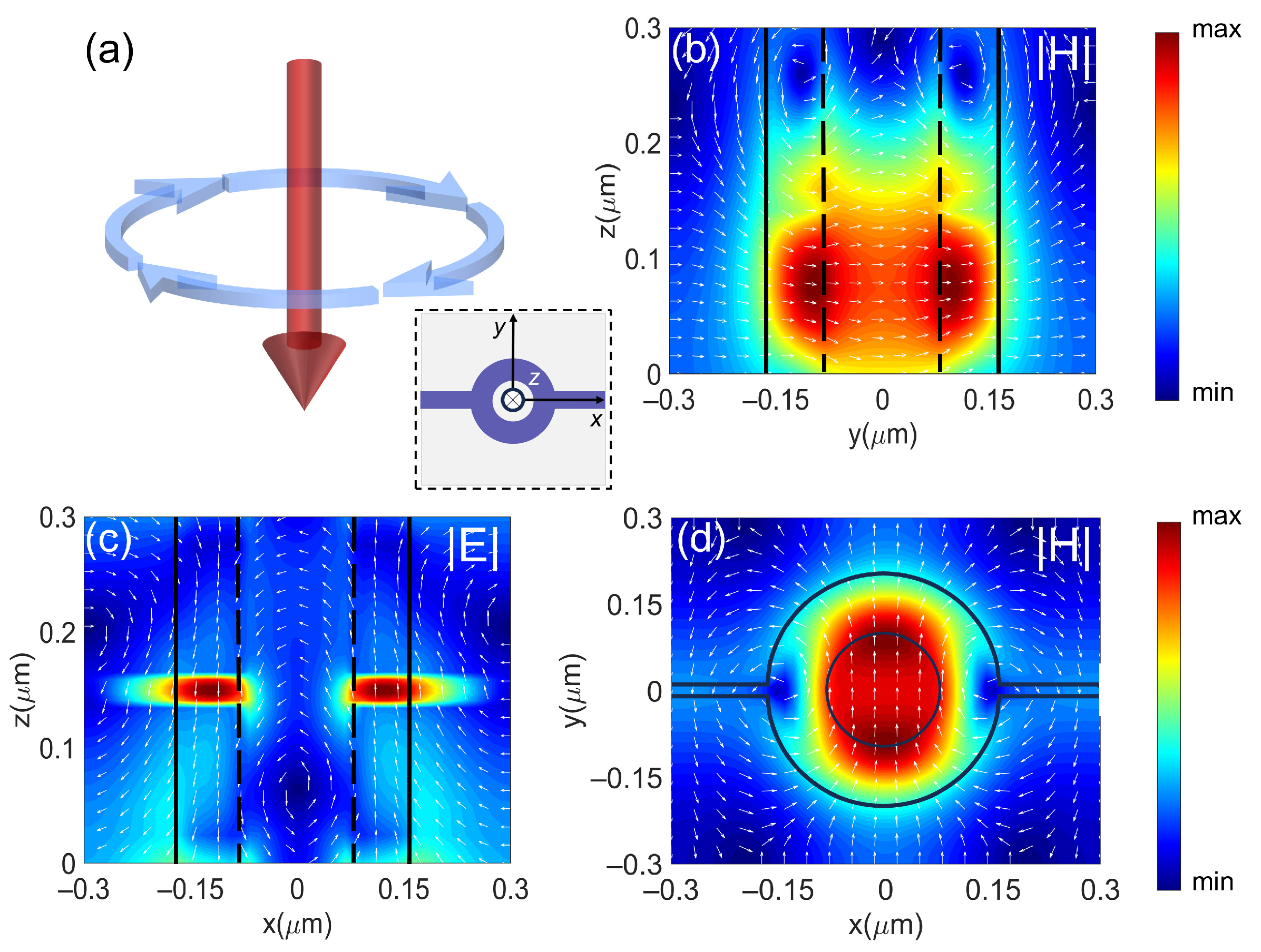
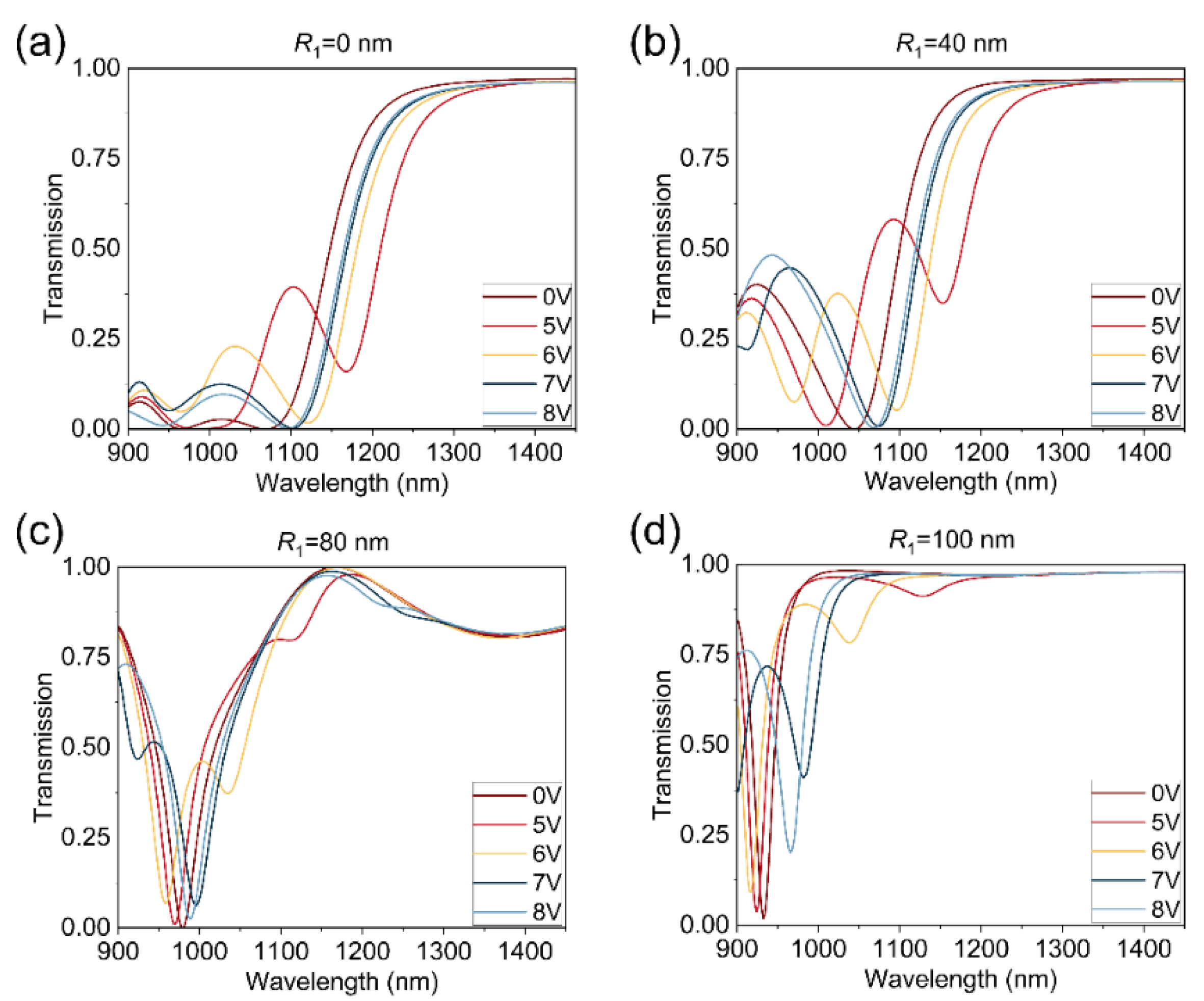
The electrically tunable metasurface is schematically shown in Figure 1. According to the charge conservation, the Si-Al2O3-ITO heterojunction can be regarded as a non-ideal parallel plate capacitor composed of the ITO layer and the Si layer acting as semiconductor plates, with equal and opposite induced charges [18]. Herein, the ITO layer is degenerately n-type doped with a background carrier concentration of 3 × 1020 cm−3, while the Si layer is heavily n-type doped with a background carrier concentration [19] of 1 × 1019 cm−3. The Si layer serves as the electrode which ensures the presence of sufficient free electrons to conduct current through the introduction of impurities (e.g., arsenic or phosphorus), thus enabling it to be utilized as a bias electrode for applying voltage to the ITO layer. To avoid applying bias individually to each nanoring, Si nanorings in the same column are connected by nanobars in the x-direction and controlled by the same voltage from one side. The strong Mie resonance is excited with TE- or TM-polarized light (polarized along or perpendicular to the nanobars) and is almost unaffected by the nanobars. Upon applying voltage to the metasurface, the formation of an electron accumulation layer at the ITO-Al2O3 interface enhances the interaction between light and matter, thereby altering the resonant properties of the metasurface. In this design, the refractive index of ITO is simulated using the Drude model [20], while the refractive indices of Si, Al2O3, and SiO2 are obtained from experimental data [20].
To determine the effect of applied voltages on Mie resonance modes, we first simulate the carrier concentration distribution of ITO under different bias voltages. As shown in Figure 2a, the same positive voltage is applied to the top and bottom Si layers, while the ITO layer is grounded (diagram of applying a voltage from one side of the metasurface is shown in Supplementary Note S1). For different bias voltages, the spatial distribution of carrier concentration in the accumulation layer can be calculated by solving the Poisson equation and the electron–hole drift-diffusion equation. As depicted in Figure 2b, increasing the applied bias voltage from 0 V to 8 V results in an increase in carrier concentration at the ITO-Al2O3 interface from 3 × 1020 cm−3 to 2.1 × 1021 cm−3. The accumulation of carrier concentration at the ITO-Al2O3 interface decays exponentially with distance, leading to an effective thickness of the accumulation layer of approximately ≈ 1 nm. The slight accumulation of carrier concentration at the ITO-Al2O3 interface under zero bias voltage is attributed to the difference in the work function of doped Si and ITO, resulting in a band-bending effect. In this model, the dielectric constant [21] of ITO is 9.3, the bandgap [22] is 2.8 eV, and the work function [16] is 6.4 eV.
After solving the Poisson equation and the drift-diffusion equation, the spatial distribution of carrier concentration within the active region of ITO is transformed into a spatial distribution of dielectric constant using a dispersion model, which can be subsequently incorporated into optical simulations. The dielectric constant of ITO can be obtained from the Drude model [20]:
ε ITO = ε ω p 2 / ( ω 2 + i ω Γ )
ω p 2 = N e 2 ε 0 m *
where ε is the high-frequency dielectric constant, Γ is the damping constant, and m* is the effective mass of electrons, with m0 representing the electron rest mass [23]. Here we have values of ε = 3.9, Γ = 100 THz, and m* = 0.35 × m0, where m0 represents the electron’s rest mass.

3. Results

As shown in Figure 3, to demonstrate the effect of bias voltage on the metasurface, we employ finite-difference time-domain (FDTD) simulations to obtain the transmission spectrum under 0 V and 7 V bias voltage. For ease of calculation, we divide the ITO layer into finite intervals, set the average electron concentration in an interval as the electron concentration of the interval, and calculate the dispersion curve by the Drude model. We use nanoring units with an inner radius R1 = 80 nm and an outer radius R2 = 160 nm, with TE-polarized incident light with wavelengths of 900–1450 nm. The results show that without applied bias voltage, the transmission spectrum of the metasurface exhibits a transmission dip at a wavelength of 978 nm. When a bias voltage of 7 V is applied, the carrier concentration in ITO increases, forming an ENZ (epsilon-near-zero) region at the Al2O3-ITO interface. The electric field is significantly enhanced within the accumulation layer, resulting in a noticeable change in the resonance characteristics of the metasurface, leading to the transmission spectrum splitting into two valleys with lowest transmittance values of 995.3 nm and 924.8 nm.
For nanoparticles composed of high-index materials such as Si, the resonances are predominantly induced by Mie scattering. To analyze the changes in modes before and after applying voltage, we calculated the far-field scattering of this metasurface structure using multipole expansion. The center of the decomposition is located at x, y = 0 μm, and z = 0.15 μm. The decomposition takes into account the spherical ring and the bars. Far-field scattering refers to the electromagnetic radiation re-emitted by various multipole modes within the nanostructure under plane wave illumination in periodic arrangements [24]. The predominant multipole modes include electric dipole (ED), magnetic dipole (MD), electric quadrupole (EQ), magnetic quadrupole (MQ), and toroidal dipole (T) modes [25] (see Supplementary Note S2). In a dielectric nanoparticle, magnetic dipole resonance (MD) arises from the excitation of a specific electromagnetic mode within the particle, characterized by a circular displacement current of the electric field. As shown in Figure 3c, without applied voltage, the MD mode dominates the transmission peak at 978 nm. Meanwhile, as depicted in Figure 3d, after applying bias voltage, the resonance peaks observed at wavelengths of 924 nm and 995 nm are primarily influenced by the MD mode (more analysis of spectral splitting is provided in Supplementary Note S3).
To verify the excitation of the MD mode, we simulate the field distributions inside the metasurface unit. Figure 4a is a schematic of the magnetic dipole pattern, which can be represented by a ring current (blue arrow). Currents flow in a ring path, creating a magnetic field perpendicular to the plane of the ring current (red arrow). Figure 4b,c illustrate the normalized magnetic field intensity (cross-section in the y-z plane) and electric field intensity (cross-section in the x-z plane), respectively, for λ = 924 nm and a bias voltage of 7 V under TE-polarized incident light. Figure 4d presents the magnetic field distribution in the x-y plane. The white arrows in Figure 4d represent displacement currents, while the dark dashed lines indicate the structural outline. From the magnetic field distribution in Figure 4d, we observe a strong magnetic field distribution within the nanoring, accompanied by circulating displacement currents inside the nanoring, as shown in Figure 4c. These results verify that the Mie resonance at λ = 924 nm is induced by the magnetic dipole mode. The near-field distribution at 924 nm without the bias and the in the case of 995 nm (with/without the bias) are shown in Supplementary Note S4.
To investigate the relationship between the transmission spectrum and structural parameters, we conduct a parameter sweep over the inner radius of the nanorings. While keeping the outer radius constant at 160 nm, we vary the inner radius to 0 nm, 40 nm, 80 nm, and 100 nm, with bias voltages of 0 V, 5 V, 6 V, 7 V, and 8 V, respectively. The incident light is TE-polarized. The transmission spectrum of the metasurface as a function of voltage and inner radius are shown in Figure 5. By increasing the inner radius, we observe that, similar to Figure 3b, the transmission spectra still exhibit two dips under different voltages, one of which is more prominent while the other peak is smaller. It is noteworthy that the quality factor (Q-value) of the larger transmission dip increases with increasing inner radius, and the resonance region gradually blueshifts. Compared with the periodic Si disk structure, the electric field of the periodic Si ring structure is more localized, resulting in a higher Q value of the transmission spectrum and a higher modulation depth, as shown in Figure 5 (more details about modulation depth calculations are provided in Supplementary Note S5). When the inner radius is 40 nm, the metasurface exhibits a large range of resonance peak shifts with increasing voltage. As the inner radius continues to increase, the resonance peak shift of the transmission spectrum decreases with increasing applied voltage, while the quality factor gradually increases. When the inner radius reaches 100 nm, the disparity between the inner and outer radius is small, and the electric field becomes more localized in the accumulation layer of ITO in the nanorings, resulting in the narrowest spectral bandwidth. Since the distribution of Mie resonance modes is directly related to the radius difference of the nanoring array, careful selection of geometric factors of the nanoring array and applied voltage magnitude allows for the obtaining of the desired wavelength and the desired depth of the transmission dip.

4. Conclusions

This paper introduces an innovative design of the electrically tunable metasurface consisting of a series of Si nanorings with ITO sandwiched between them on a glass substrate. By applying a certain voltage to the metasurface, the excitation condition of the magnetic dipole (MD) mode changes, thereby affecting the optical performance of the metasurface. Further studies have shown that significant electrical modulation of the transmission spectrum can be achieved by selecting the inner and outer radius as well as the period of the nanorings. This design not only avoids the absorption losses of metallic nanostructures, but also allows for dynamic control of the transmission spectrum rather than the reflection spectrum. The device also shows compatibility with CMOS technology. We envisage that the device can be fabricated as silicon-based sensors and spectral reconstruction filters.

Supplementary Materials

The following supporting information can be downloaded at https://www.mdpi.com/article/10.3390/nano14191606/s1, Figure S1. Diagram of applying a voltage from one side of the metasurface. Figure S2. Transmission spectrum of the metasurface with one accumulation layer under TE-polarized incident light with a 7 V applied bias voltage. Figure S3. (a) The structure diagram in x-y plane. (b) Near-field distribution of the magnetic field component (|H|) (cross-section in the y-z plane) at a wavelength of 995 nm under 7 V bias voltage, where the outline of the nanoring is represented by dark dashed lines, the field directions is represented by white arrows. (c) Near-field distribution of the electric field component (|E|) (cross-section in the x-z plane) and displacement current at a wavelength of 995 nm under 7 V bias voltage. (d) Magnetic field distribution in the x-y plane at a wavelength of 995 nm under 7 V bias voltage. Figure S4. (a) and (d) Near-field distribution of the electric field component (|E|) (cross-section in the x-z plane) and displacement current at a wavelength of 924 nm and 995 nm under 7 V bias voltage. (b) and (e) Near-field distribution of the magnetic field component (|H|) (cross-section in the y-z plane) at a wavelength of 924 nm and 995 nm under 7 V bias voltage, where the outline of the nanoring is represented by dark dashed lines, the field directions is represented by white arrows. (c) and (f) Magnetic field distribution in the x-y plane at a wavelength of 924 nm and 995 nm under 7 V bias voltage. Figure S5. The modulation depth under different voltages when R1 = 0.04 μm. Figure S6. Variation of (a) hole concentration (b) electron concentration in the Si accumulation layer as a function of applied a bias voltage and distance from the Si-Al2O3 interface. Figure S7. The real and imaginary parts of the Si permittivity located near the Si-Al2O3 surface at 8 V voltage. Figure S8. Dispersion curve of ITO at the closest layer to the Al2O3 layer (a) with a 0 V voltage and (b) with a 7 V applied bias voltage. Table S1. Comparison of proposed and reported metasurfaces for dynamic regulation. Refs [19,20,24,26,27,28,29,30,31] are cited in the supplementary materials.

Author Contributions

Conceptualization, R.M. and D.W.; Software, R.M.; Validation, R.M., Y.M. and P.L.; Resources, D.W.; Writing—original draft, R.M.; Writing—review & editing, Y.M., P.L., D.L. and D.W.; Supervision, D.W.; Project administration, R.M.; Funding acquisition, D.W. All authors have read and agreed to the published version of the manuscript.

Funding

This work was supported in part by the National Natural Science Foundation of China (Grant Nos. 62175200 and 61975165) and the National Key Research and Development Program of China (2022YFA1404800).

Data Availability Statement

The data that support the findings of this study are available from the corresponding authors upon reasonable request.

Conflicts of Interest

The authors declare no conflicts of interest.

References

  1. Koshelev, K.; Tang, Y.T.; Li, K.F.; Choi, D.Y.; Li, G.X.; Kivshart, Y. Nonlinear Metasurfaces Governed by Bound States in the Continuum. ACS Photon. 2019, 6, 1639–1644. [Google Scholar] [CrossRef]
  2. Huang, L.L.; Chen, X.Z.; Mühlenbernd, H.; Li, G.X.; Bai, B.F.; Tan, Q.F.; Jin, G.F.; Zentgraf, T.; Zhang, S. Dispersionless Phase Discontinuities for Controlling Light Propagation. Nano Lett. 2012, 12, 5750–5755. [Google Scholar] [CrossRef]
  3. Huang, L.L.; Chen, X.Z.; Mühlenbernd, H.; Zhang, H.; Chen, S.M.; Bai, B.F.; Tan, Q.F.; Jin, G.F.; Cheah, K.W.; Qiu, C.W.; et al. Three-dimensional optical holography using a plasmonic metasurface. Nat. Commun. 2013, 4, 2808. [Google Scholar] [CrossRef]
  4. Deng, L.G.; Deng, J.; Guan, Z.Q.; Tao, J.; Chen, Y.; Yang, Y.; Zhang, D.X.; Tang, J.B.; Li, Z.Y.; Li, Z.L.; et al. Malus-metasurface-assisted polarization multiplexing. Light Sci. Appl. 2020, 9, 101. [Google Scholar] [CrossRef]
  5. Zheng, G.; Mühlenbernd, H.; Kenney, M.; Li, G.; Zentgraf, T.; Zhang, S. Metasurface holograms reaching 80% efficiency. Nat. Nanotechnol. 2015, 10, 308–312. [Google Scholar] [CrossRef]
  6. Tognazzi, A.; Rocco, D.; Gandolfi, M.; Locatelli, A.; Carletti, L.; De Angelis, C. High Quality Factor Silicon Membrane Metasurface for Intensity-Based Refractive Index Sensing. Optics 2021, 2, 193–199. [Google Scholar] [CrossRef]
  7. Du, K.; Barkaoui, H.; Zhang, X.D.; Jin, L.M.; Song, Q.H.; Xiao, S.M. Optical metasurfaces towards multifunctionality and tunability. Nanophotonics 2022, 11, 1761–1781. [Google Scholar] [CrossRef]
  8. Ou, X.; Zeng, T.; Zhang, Y.; Jiang, Y.; Gong, Z.; Fan, F.; Jia, H.; Duan, H.; Hu, Y. Tunable Polarization-Multiplexed Achromatic Dielectric Metalens. Nano Lett. 2022, 22, 10049–10056. [Google Scholar] [CrossRef]
  9. Wen, Y.; Zhang, Q.; He, Q.; Zhang, F.; Xiong, L.; Zhang, F.; Fu, G.; Xu, J.; Pu, M.; Luo, X. Shortening Focal Length of 100-mm Aperture Flat Lens Based on Improved Sagnac Interferometer and Bifacial Liquid Crystal. Adv. Opt. Mater. 2023, 11, 2300127. [Google Scholar] [CrossRef]
  10. Hu, Y.; Ou, X.; Zeng, T.; Lai, J.; Zhang, J.; Li, X.; Luo, X.; Li, L.; Fan, F.; Duan, H. Electrically Tunable Multifunctional Polarization-Dependent Metasurfaces Integrated with Liquid Crystals in the Visible Region. Nano Lett. 2021, 21, 4554–4562. [Google Scholar] [CrossRef]
  11. Sabri, R.; Forouzmand, A.; Mosallaei, H. Genetically optimized dual-wavelength all-dielectric metasurface based on double-layer epsilon-near-zero indium-tin-oxide films. J. Appl. Phys. 2020, 128, 223101. [Google Scholar] [CrossRef]
  12. Cai, Z.; Liu, Y. Near-Infrared Reflection Modulation Through Electrical Tuning of Hybrid Graphene Metasurfaces. Adv. Opt. Mater. 2022, 10, 2102135. [Google Scholar] [CrossRef]
  13. Tian, J.; Adamo, G.; Liu, H.; Wu, M.; Klein, M.; Deng, J.; Ang, N.S.S.; Paniagua-Dominguez, R.; Liu, H.; Kuznetsov, A.I.; et al. Phase-Change Perovskite Microlaser with Tunable Polarization Vortex. Adv. Mater. 2023, 35, e2207430. [Google Scholar] [CrossRef] [PubMed]
  14. Pianelli, A.; Caligiuri, V.; Dudek, M.; Kowerdziej, R.; Chodorow, U.; Sielezin, K.; De Luca, A.; Caputo, R.; Parka, J. Active control of dielectric singularities in indium-tin-oxides hyperbolic metamaterials. Sci. Rep. 2022, 12, 16961. [Google Scholar] [CrossRef]
  15. Dayal, G.; Ramakrishna, S.A. Broadband infrared metamaterial absorber with visible transparency using ITO as ground plane. Opt. Express 2014, 22, 15104–15110. [Google Scholar] [CrossRef] [PubMed]
  16. Huang, Y.W.; Lee, H.W.; Sokhoyan, R.; Pala, R.A.; Thyagarajan, K.; Han, S.; Tsai, D.P.; Atwater, H.A. Gate-Tunable Conducting Oxide Metasurfaces. Nano Lett. 2016, 16, 5319–5325. [Google Scholar] [CrossRef]
  17. Park, J.; Jeong, B.G.; Kim, S.I.; Lee, D.; Kim, J.; Shin, C.; Lee, C.B.; Otsuka, T.; Kyoung, J.; Kim, S.; et al. All-solid-state spatial light modulator with independent phase and amplitude control for three-dimensional LiDAR applications. Nat. Nanotechnol. 2021, 16, 69–76. [Google Scholar] [CrossRef]
  18. Forouzmand, A.; Salary, M.M.; Kafaie Shirmanesh, G.; Sokhoyan, R.; Atwater, H.A.; Mosallaei, H. Tunable all-dielectric metasurface for phase modulation of the reflected and transmitted light via permittivity tuning of indium tin oxide. Nanophotonics 2019, 8, 415–427. [Google Scholar] [CrossRef]
  19. Forouzmand, A.; Mosallaei, H. Tunable dual-band amplitude modulation with a double epsilon-near-zero metasurface. J Opt 2020, 22, 094001. [Google Scholar] [CrossRef]
  20. Palik, E.D. Handbook of Optical Constants of Solids; Academic press: Cambridge, MA, USA, 1998; Volume 3. [Google Scholar]
  21. Yi, F.; Shim, E.; Zhu, A.Y.; Zhu, H.; Reed, J.C.; Cubukcu, E. Voltage tuning of plasmonic absorbers by indium tin oxide. Appl. Phys. Lett. 2013, 102, 221102. [Google Scholar] [CrossRef]
  22. Klein, A.; Korber, C.; Wachau, A.; Sauberlich, F.; Gassenbauer, Y.; Harvey, S.P.; Proffit, D.E.; Mason, T.O. Transparent Conducting Oxides for Photovoltaics: Manipulation of Fermi Level, Work Function and Energy Band Alignment. Materials 2010, 3, 4892–4914. [Google Scholar] [CrossRef] [PubMed]
  23. Kafaie Shirmanesh, G.; Sokhoyan, R.; Pala, R.A.; Atwater, H.A. Dual-Gated Active Metasurface at 1550 nm with Wide (>300 degrees) Phase Tunability. Nano Lett. 2018, 18, 2957–2963. [Google Scholar] [CrossRef] [PubMed]
  24. Alaee, R.; Rockstuhl, C.; Fernandez-Corbaton, I. An electromagnetic multipole expansion beyond the long-wavelength approximation. Opt. Commun. 2018, 407, 17–21. [Google Scholar] [CrossRef]
  25. Savinov, V.; Fedotov, V.A.; Zheludev, N.I. Toroidal dipolar excitation and macroscopic electromagnetic properties of metamaterials. Phys. Rev. B 2014, 89, 205112. [Google Scholar] [CrossRef]
  26. Fan, S.; Suh, W.; Joannopoulos, J.D. Temporal coupled-mode theory for the Fano resonance in optical resonators. J. Opt. Soc. Am. A 2003, 20, 569–572. [Google Scholar] [CrossRef]
  27. Xie, Z.T.; Wu, J.Y.; Fu, H.Y.; Li, Q. Tunable Electro- and All-Optical Switch Based on Epsilon-Near-Zero Metasurface. IEEE Photon. J. 2020, 12, 1–10. [Google Scholar] [CrossRef]
  28. Shoaei, M.; Moravvej-Farshi, M.K.; Yousefi, L. All-optical switching of nonlinear hyperbolic metamaterials in visible and near-infrared regions. J. Opt. Soc. Am. B 2015, 32, 2358–2365. [Google Scholar] [CrossRef]
  29. Kim, S.J.; Brongersma, M.L. Active flat optics using a guided mode resonance. Opt. Lett. 2017, 42, 5–8. [Google Scholar] [CrossRef]
  30. Howes, A.; Wang, W.; Kravchenko, I.; Valentine, J. Dynamic transmission control based on all-dielectric Huygens metasurfaces. Optica 2018, 5, 787–792. [Google Scholar] [CrossRef]
  31. Zhang, J.; Yang, J.; Schell, M.; Anopchenko, A.; Tao, L.; Yu, Z.; Lee, H.W.H. Gate-tunable optical filter based on conducting oxide metasurface heterostructure. Opt. Lett. 2019, 44, 3653–3656. [Google Scholar] [CrossRef]
Figure 1. Schematic of the electrically tunable metasurface composed of Si nanorings. (a) Three-dimensional structure of the metasurface. The substrate is SiO2 and the Si nanorings have intermediate layers of Al2O3/ITO/Al2O3. Adjacent Si nanorings in the same column are connected by Si nanobars. By controlling the magnitude of the applied bias voltage, the metasurface can modulate the transmission spectrum over a significant range in the near-infrared wavelength band. (b) Top view (x-y plane) of the structural unit. The inner and outer radii of the rings are represented by R1 and R2, respectively, and the width of the nanobars is denoted as w. (c) Cross-sectional view (y-z plane) of the structural unit. The period of the structural unit is P, and the thickness of both the upper and lower Si layers is hSi, while that of the upper and lower Al2O3 layers is hAl2O3. The thickness of the ITO layer is hITO. Throughout this paper, the following parameters are kept constant: w = 20 nm, P = 600 nm, hSi = 140 nm, hAl2O3 = 5 nm, hITO = 10 nm.
Nanomaterials 14 01606 g001
Figure 2. Schematic representation of biasing for the electrically tunable metasurface, and simulation of carrier concentration and dielectric constant of ITO. (a) Schematic diagram of the biasing scheme, where the voltage is applied to the Si layer and the ITO layer is grounded. (b) Variation of electron concentration in the ITO accumulation layer as a function of applied bias voltage and distance from the ITO-Al2O3 interface. (c) Real part and (d) imaginary part of the dielectric constant of ITO as functions of voltage and distance from the ITO-Al2O3 interface at the wavelength of 1038 nm, with an applied bias voltage ranging from 0 V to 8 V.
Nanomaterials 14 01606 g002
Figure 3. Transmission spectrum of the metasurface and corresponding scattering cross-sections obtained at different voltages. In this part, we set the inner radius and outer radius of nanoring units to be 80 nm and 160 nm, respectively. (a) Transmission spectrum of the metasurface under TE-polarized incident light without an applied bias voltage and (b) with a 7 V applied bias voltage. (c) Calculated scattered cross-sections for electromagnetic multipoles of the metamaterial array without applied bias voltage and (d) with a 7 V applied bias voltage. The plot displays the first five multipoles: magnetic dipole (MD), electric dipole (ED), toroidal dipole (T), electric quadrupole (EQ), and magnetic quadrupole (MQ).
Nanomaterials 14 01606 g003
Figure 4. (a) Charge distribution and current flow of the MD mode. (b) Near-field distribution of the magnetic field component (|H|) (cross-section in the y-z plane) at a wavelength of 924 nm under 7 V bias voltage, where the outline of the nanoring is represented by dark dashed lines and the field directions are represented by white arrows. (c) Near-field distribution of the electric field component (|E|) (cross-section in the x-z plane) and displacement current at a wavelength of 924 nm under 7 V bias voltage. (d) Magnetic field distribution in the x-y plane at a wavelength of 924 nm under 7 V bias voltage. Max represents the maximum of E/E0 and H/H0, and min represents the minimum of E/E0 and H/H0.
Nanomaterials 14 01606 g004
Figure 5. Transmission spectrum of the electrically tunable metasurface under different voltages, with inner radius R1 = 0 nm, 40 nm, 80 nm, and 100 nm, and outer radius R2 = 160 nm. The light source is a normally incident TE-polarized plane wave.
Nanomaterials 14 01606 g005
Disclaimer/Publisher’s Note: The statements, opinions and data contained in all publications are solely those of the individual author(s) and contributor(s) and not of MDPI and/or the editor(s). MDPI and/or the editor(s) disclaim responsibility for any injury to people or property resulting from any ideas, methods, instructions or products referred to in the content.

