Article

Ultrastable and Low-Threshold Two-Photon-Pumped Amplified Spontaneous Emission from CsPbBr3/Ag Hybrid Microcavity

1
School of Optoelectronic Engineering, Guangdong Polytechnic Normal University, Guangzhou 510665, China
2
School of Material Science and Engineering, Hanshan Normal University, Chaozhou 521041, China
*
Authors to whom correspondence should be addressed.
Nanomaterials 2024, 14(20), 1622; https://doi.org/10.3390/nano14201622
Submission received: 7 September 2024 / Revised: 23 September 2024 / Accepted: 9 October 2024 / Published: 10 October 2024
(This article belongs to the Special Issue Nanostructured Materials for Photonic and Plasmonic Applications)

Abstract

:
Halide perovskite materials have garnered significant research attention due to their remarkable performance in both photoharvesting photovoltaics and photoemission applications. Recently, self-assembled CsPbBr3 superstructures (SSs) have been demonstrated to be promising lasing materials. In this study, we report the ultrastable two-photon-pumped amplified stimulated emission from a CsPbBr3 SS/Ag hybrid microcavity with a low threshold of 0.8 mJ/cm2 at room temperature. The experimental results combined with numerical simulations show that the CsPbBr3 SS exhibits a significant enhancement in the electromagnetic properties in the hybrid microcavity on Ag film, leading to the uniform spatial temperature distribution under the irradiation of a pulsed laser, which is conducive to facilitate the recrystallization process of the QDs and improve their structural integrity and optical properties. This study provides a new idea for the application of CsPbBr3/Ag hybrid microcavity in photonic devices, demonstrating its potential in efficient optical amplification and upconversion lasers.

1. Introduction

Achieving visible lasers by means of infrared two/multiphoton pumping has been demonstrated as an effective method for frequency upconversion [1,2,3]. Compared to single-photon excitations, double/multi-photon excitation has obvious advantages such as large penetration depth, small Rayleigh scattering, and small light damage to samples [4,5,6]. However, such lasers impose stringent requirements on large optical gain and efficient multiphoton absorption [7]. This restricts the range of lasing materials to a limited selection of organic dyes [8], polymers [9], and specific inorganic semiconductor nanostructures [10]. Among the suitable systems, metal halide perovskite (CsPbX3, (X = Cl, Br and I)) has attracted extensive attention and in-depth research [11,12,13]. This new kind of semiconductor is favored for its unique advantages in the field of optoelectronics, such as its high optical absorption coefficient, tunable band gap, long carrier lifetime, and mobility, which make it show great potential in photovoltaic, light-emitting diode (LED) [14], light detector, and laser applications [15,16]. However, their usage is significantly limited by their poor stability when exposed to moisture. Very promising approaches for overcoming these limitations have been discovered in many ways, among which encapsulation in inorganic oxidized glass is a more common approach [17,18]. To date, stable and low-threshold amplified stimulated emission (ASE) has been demonstrated from CsPbX3.
As the shape, size, and heterostructures of conventional CsPbX3 are further modified, the two-photon absorption in perovskite nanomaterials may be further enhanced [19,20,21]. The self-assembly and regrowth of individual components is one of the most facile approaches [22,23,24,25]. The CsPbX3 superstructure (SS) is formed through the self-assembly of QDs driven by weak microscopic interactions, resulting in a long-range-ordered three-dimensional structure [26]. In the process of the self-assembly of QDs, lattice and surface defects are generated due to factors such as interface mismatch, stress concentration, or unstable growth conditions [7,27]. These defects will cause an increase in the non-radiative recombination rate and a decrease in quantum efficiency. In addition, the low efficiency of the two-photon absorption process, which requires a high-power excitation source, produces significant thermal effects, resulting in the thermal damage or photodegradation of the material. Therefore, the performance of two-photon-pumped ASE largely depends on the crystallinity and morphology of the CsPbX3 structure. Laser annealing is the use of laser energy to achieve the local or overall heating of the material [28,29,30,31], which can effectively repair various defective materials, so as to significantly improve the optical properties and stability of the material [32,33,34]. However, the thermal management in a CsPbX3 SS during laser annealing is necessary to avoid thermal accumulation on the surface of the CsPbX3 SSs. The application of optical microcavities shows potential in enhancing thermal control during this process [35,36,37,38,39]. It is reported that optical microcavities enhance temperature distributions, and reduce thermal damage by limiting and localizing electromagnetic fields [33,40]. It is reported that optical microcavities enhance temperature distributions, and reduce thermal damage by limiting and localizing electromagnetic fields. In addition, the resonance mode in the microcavity can improve the efficiency of energy transfer.
Herein, we formed CsPbBr3 SSs through the self-assembly of QDs, combined with silver film to prepare a CsPbBr3/Ag hybrid microcavity. Femtosecond laser annealing technology was used to eliminate SS surface defects and lattice defects. The hybrid microcavity has a plasma–photon hybrid mode, the electromagnetic environment inside the SS is redesigned, and the temperature distribution during the laser annealing process is precisely controlled to facilitate the recrystallization process of the QDs, improving their structural integrity and optical properties. The laser threshold is lowered, which achieves an efficient ASE and upconversion emission. This is of great significance for the realization of high-efficiency and low-threshold amplified spontaneous radiation and two-photon-pumped laser.

2. Materials and Methods

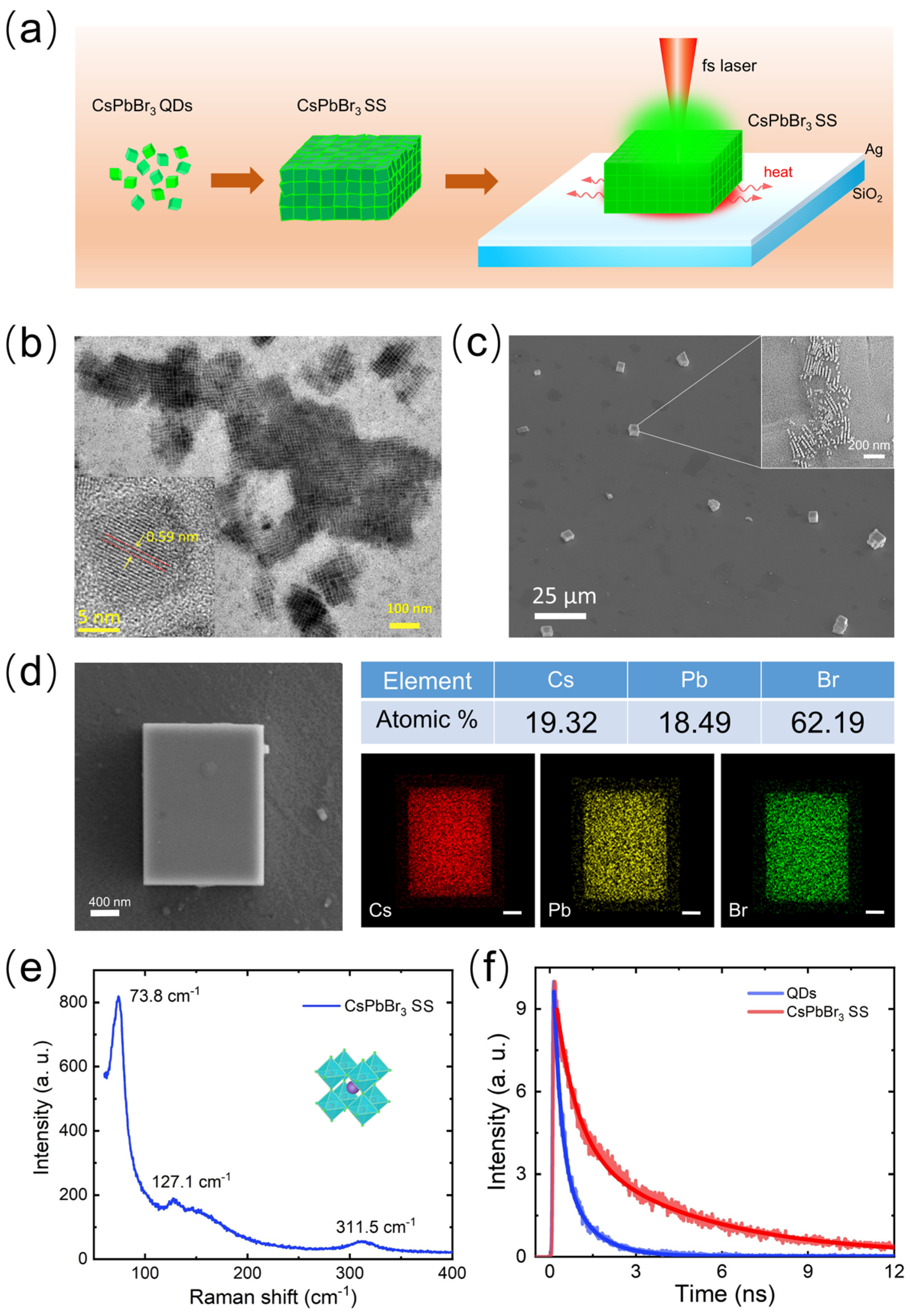
2.1. Sample Preparation and Characterization

In this work, the CsPbBr3/Ag hybrid microcavities used was fabricated by the following procedure. First, CsPbBr3 QDs were synthesized by hot-injection method. The as-prepared CsPbBr3 QD solution with the added methyl acetate was left standing at room temperature for ten days. Then, the solution was spin-coated onto a Ag/SiO2 substrate and SiO2 substrate at a rate of 4000 rpm for 40 s. The CsPbBr3 SSs were formed on the surface of the Ag film and SiO2 substrate, respectively. The morphology and component elements of CsPbBr3 SSs were characterized by a scanning electron microscope (SEM) (Hitachi SU5000, Tokyo, Japan) and energy dispersive spectroscopy (EDS) (Bruker EDS QUANTAX, Billerica, MA, USA). The PL spectra of CsPbBr3 SSs were collected by a 40× UV objective lens in a Raman spectrometer system (Horiba LabRAM HR Evolution, Tokyo, Japan) equipped with a 325 nm He-Cd laser (Kimmon, Tokyo, Japan).

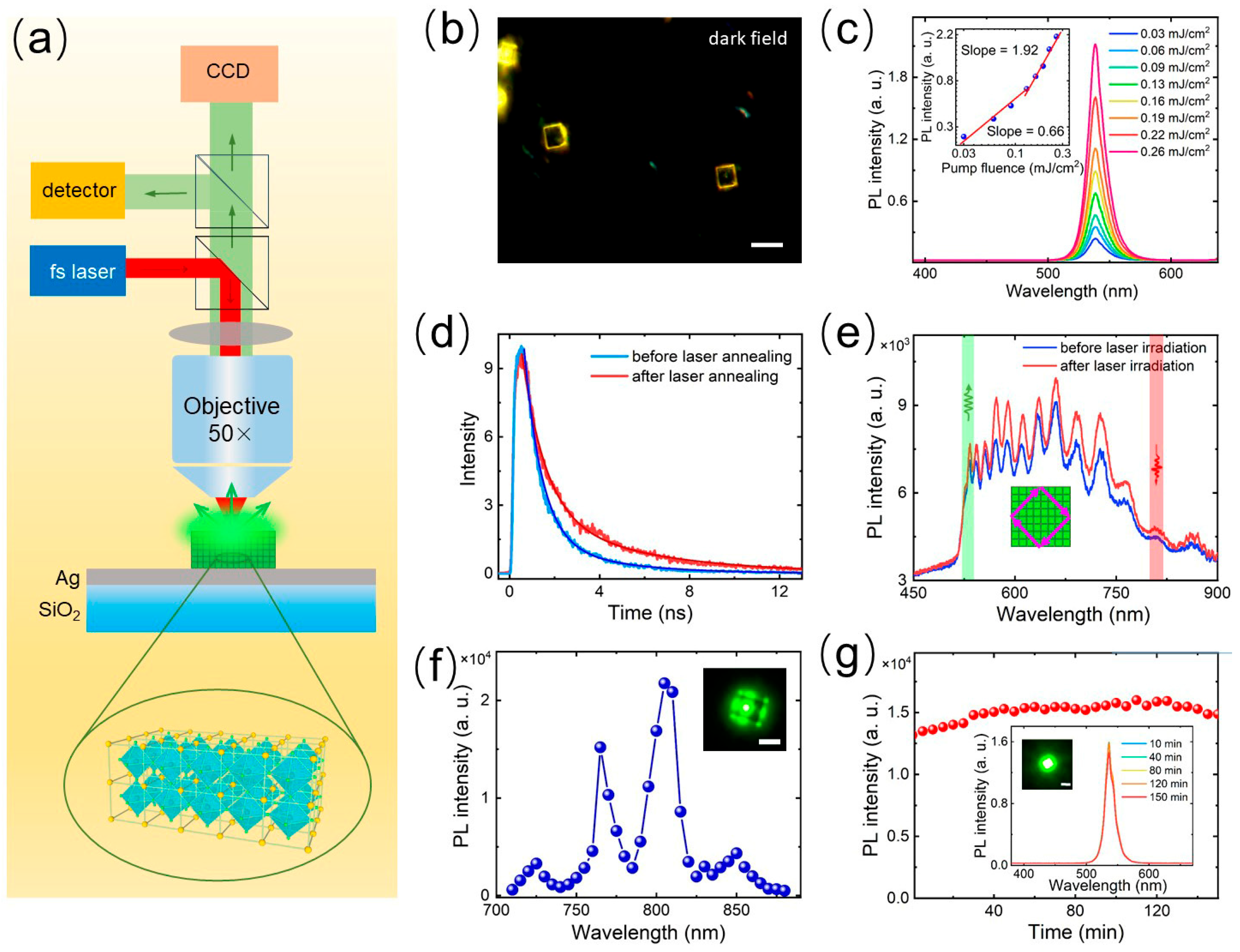
2.2. Optical Characterization of CsPbBr3/Ag Hybrid Microcavities

The 800 nm femtosecond laser (Mira 900S, Coherent, Saxonburg, PA, USA, 130 fs) was utilized to excite the CsPbBr3 microdisks (SSs). The PL spectra measurements were conducted at a high repetition rate of 76 MHz, and luminescence lifetimes were measured using a low repetition rate of 3.8 MHz (achieved via a pulse picker) in conjunction with a time-correlated single-photon counting system (lifespec II, Edinburgh Instruments, Livingston, UK). The laser light was focused onto the samples using a 50× objective lens (NA = 0.8) on an inverted microscope (Axio Observer A1, Zeiss, Oberkochen, Germany). The scattered light and photoluminescence were collected through the same objective lens and directed either to a spectrometer (SR-500i-B1, Andor, Abingdon, Oxon, UK) for spectral analysis or to a charge-coupled device (DU970N, Andor, Abingdon, Oxon, UK) for recording.

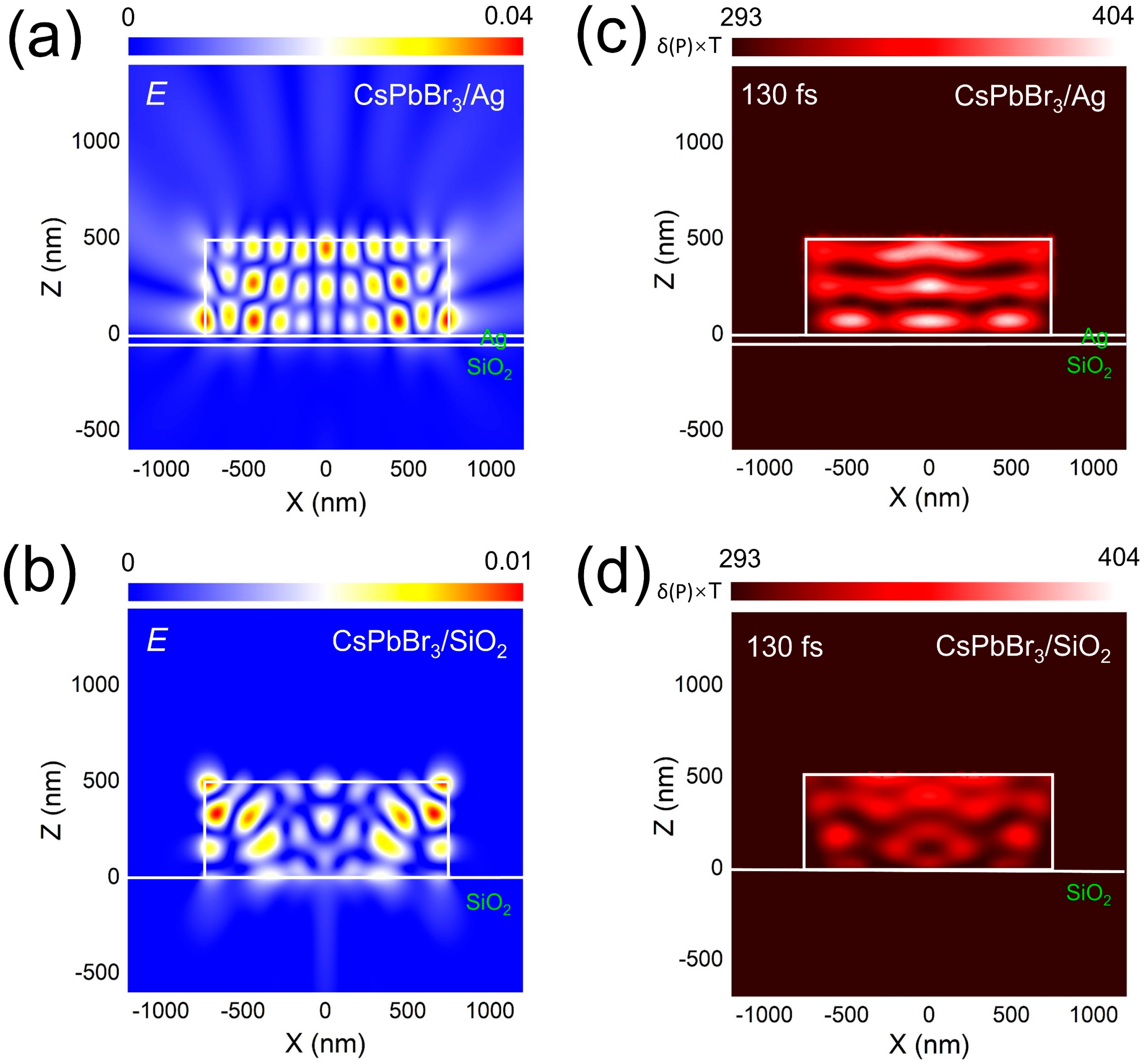
2.3. Numerical Simulation and Analytical Model

The electric field distribution of CsPbBr3 SSs placed on a thin Ag film and SiO2 substrate were numerically calculated using the finite-difference time-domain (FDTD) method (FDTD solution, https://www.lumerical.com (accessed on 1 August 2024)). The side length of the CsPbBr3 SSs is 1.5 × 1.5 μm and the height is 0.5 μm. The dielectric constants of Ag and CsPbBr3 SSs were taken from the previous literature [41,42]. The refractive index and thermal conductivity of CsPbBr3 SSs were taken from the literature. The temperature distributions inside the hybrid microcavities were calculated numerically based on the finite element method (FEM) (COMSOL Multiphysics v5.6, https://www.comsol.com (accessed on 1 August 2024)). The complex refractive index and thermal conductivity of monocrystalline CsPbBr3 were taken from the literature [12,43,44].

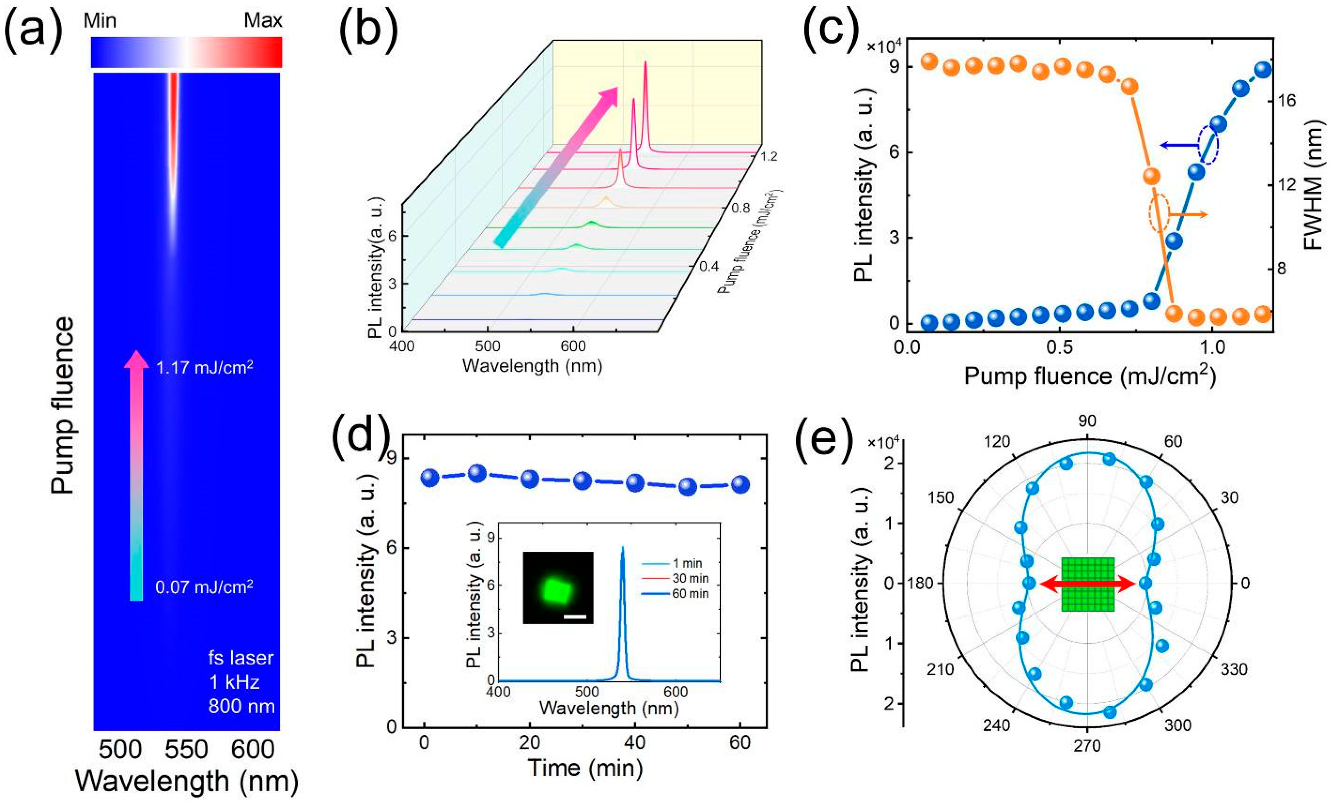
3. Results and Discussion

Figure 1a shows a schematic diagram of the CsPbBr3/Ag hybrid microcavity prepared using interfacial self-assembly, spin-coating, and post-self-assembly annealing. First, a polar solvent (acetone) is added to the CsPbBr3 QDs solution to remove the oleic acid/oleylamine ligands on the surface of QDs, thereby enhancing the weak interactions between them. This process allowed the QDs to slowly self-assemble, forming an orderly arranged microscale superstructure, known as CsPbBr3 SSs. Then, a CsPbBr3/Ag hybrid microcavity was prepared by placing a CsPbBr3 SS on the surface of the Ag film. In a previous study, the coupling between the exciton emissions of the CsPbBr3 QDs and microsphere WGM optical mode on Ag film substrate was significantly stronger than that on Au film substrate and glass substrate [16]. This is due to the lower optical loss of the silver film, and the plasmon resonance wavelength is closer to the ultraviolet region. The hybrid nanocavity structure composed of dielectric particles and metal film can form a plasma–photon mixed mode, thereby redesigning the electromagnetic environment inside the dielectric particles. The self-assembly of QDs can lead to the formation of defects, such as surface defects, lattice defects, and uneven QD coupling, which can be repaired under laser annealing. The ordered structure of CsPbBr3 SS is formed on the microscale, thus improving the crystal quality and structural integrity.
The CsPbBr3 SSs were fabricated by the self-assembly of QDs, assisted by polar solvent. Figure 1b shows the high-resolution transmission electron microscope (HR-TEM) image of pristine monodispersed CsPbBr3 QDs with an average size of ~10 nm. The HR-TEM images reveals distinct lattice fringes with an interplanar spacing of ~0.59 nm. The self-assembly of QDs is primarily driven by intermolecular forces between their aliphatic ligands. In this study, surface-bound ligands, which are highly responsive to polar solvents, were utilized to assemble CsPbBr3 SSs. Figure 1c shows that the CsPbBr3 SSs appear as cuboids with micrometer edges. There are still some QDs remaining on the surface of SSs that are not involved in synthesis, but they also show regular arrangement. In Figure 1d, the SEM image reveals that the CsPbBr3 SSs have a smooth and flat surface, featuring a microscale superstructure with an orderly arrangement. The elemental mapping of a typical CsPbBr3 SS based on energy-dispersive spectroscopy (EDS) is presented. The atomic ratio of Cs–Pb–Br is very close to the stoichiometry of 1:1:3. In Figure 1e, we present the Raman spectrum of the CsPbBr3 SSs. As reported previously, a strong peak at 73.8 cm−1 corresponds to the acoustic phonon mode, which is attributed to the vibration mode of the [PbBr6]4− octahedron. Additionally, a broad peak at 127.1 cm−1 is associated with the motion of Cs+ cations, and the broad peak at 311.5 cm−1 is related to the second-order phonon mode of the octahedron [45]. We also measured the luminescence lifetimes of CsPbBr3 QDs and CsPbBr3 SSs, as shown in Figure 1f. The PL decay curves were fitted using a bi-exponential decay function with two-time constants (τ1 and τ2). The results indicate that the luminescence lifetime of the CsPbBr3 SSs (τ1 = 2.3 ns, τ2 = 4.5 ns) is significantly longer than that of the QDs (τ1 = 0.45 ns, τ2 = 0.93 ns). This extended luminescence lifetime is due to the suppression of nonradiative recombination, as the interactions between QDs reduce nonradiative pathways and enhance radiative recombination. Moreover, the CsPbBr3 SS induces photon localization effects, which decrease the energy exchange efficiency between the QDs and their surrounding environment, leading to prolonged fluorescence lifetimes. A comparison of the PL peaks between the QDs and the microdisks reveals a redshift in the peak position. This redshift can be attributed to electronic coupling within the superlattice, which causes the splitting of the quantized carrier energy levels of individual QDs and the formation of quasi-collective electronic bands.
Laser annealing has been widely used to repair the defects of micro and nano materials. It uses high-energy laser pulses to heat the surface of the material instantaneously, prompting the local temperature to rise rapidly so that the atoms in the lattice are rearranged and thus repair or reduce the defects in the material. The experimental setup used in this work is illustrated in Figure 2a [33,46,47,48]. The backscattering and PL of CsPbBr3 SSs were collected with a microscope, analyzed with a spectrometer, and images were collected with CCD. Figure 2b shows the dark field image of a CsPbBr3 SS placed on the surface of Ag film. The CsPbBr3 SS was annealed by using 800 nm femtosecond laser pulsed with repetition rate of 76 MHz at a power fluence of 0.2 mJ/cm2. In this case, using conventional point excitation, the CsPbBr3 SS was irradiated for 1 min. Figure 2c shows the upconversion PL spectrum of CsPbBr3 SS under different power. To confirm the two-photon absorption (TPA) and emission process of CsPbBr3 SSs, we show the dependence of PL intensity on laser power, noting that the slope of intensity increase was significantly lower at low laser power compared to high laser power. This behavior is mainly due to the significant changes between the QDs within the CsPbBr3 SSs, including TPA, field enhancement, and emission quantum efficiency. In this case, part of the energy absorbed is used to repair the internal defects of CsPbBr3 SSs, thus forming an atomic-scale-ordered structure in the microscale structure. After laser annealing, the quadratic relationship between PL intensity and excitation intensity clearly confirms the two-photon absorption and emission process. In Figure 2d, we show the luminescence lifetimes measured for CsPbBr3 SSs before and after laser annealing. It was found that the luminescence lifetime of CsPbBr3 SSs after laser annealing (τ1 = 1.5 ns, τ2 = 4.7 ns) is significantly longer than that before laser annealing (τ1 = 0.9 ns, τ2 = 3.3 ns). Additionally, we were surprised to observe an increase in scattering intensity and a blue shift in the peak position after annealing, as shown in Figure 2e. This indicates that some voids and vacancies still exist within the CsPbBr3 SSs, and the localized heating caused by the laser annealing rearranges or passivates uncoordinated ions on the QDs surfaces, reducing the number of surface defect states and promoting the recrystallization process. Then, a CsPbBr3 SS/Ag hybrid nanocavity has good crystallization quality after laser annealing and can achieve high-stability fluorescence emission. In Figure 2f, we further investigated the dependence of PL intensity on an excitation wavelength, finding that the maximum efficiency was achieved at 800 nm, which coincides with the optical resonance peak of the CsPbBr3/Ag hybrid microcavity. This resonance-enhancement effect increases the absorption efficiency of the CsPbBr3 SS at specific wavelengths, which is crucial for achieving low-threshold spontaneous emission. We further studied the stability of fluorescence emission. Figure 2g shows that, when a 800 nm, 76 MHz pulsed laser is irradiated with 1.1 mJ/cm2 for about 2.5 h, the light intensity of CsPbBr3 SS remains stable and has good light stability.
It is well known that the electric field has an important effect on temperature distribution, especially at the micron- and nanoscale. The electric field has a profound effect on the regulation of local temperature, which is a very interesting and complex problem. Until now, however, accurately measuring the temperature inside a micron cavity has been a challenge. Therefore, we simulated the transient temperature distribution within CsPbBr3 SSs on different substrates under pulsed femtosecond laser irradiation, using a femtosecond laser two-temperature model [49]. In Figure 3a, we present the XZ-plane electric field distribution of a CsPbBr3 microdisk (SS) placed on a Ag thin film at a wavelength of λ = 540 nm, which corresponds to the emission wavelength of CsPbBr3. Here, the side length and thickness of the cubic SS are assumed to be 1.5 μm and 0.5 μm, respectively. Notably, the electric field distribution within the CsPbBr3 SS exhibits standing wave patterns in both the x and z directions. This regular electric field distribution arises from the interaction between higher-order Mie resonances and the whispering gallery mode (WGM) or Fabry–Pérot (F–P) resonances supported by the hybrid microcavity [16]. The electric field distribution within a CsPbBr3 SS on a glass substrate, as shown in Figure 3b, is irregular, with indistinct resonance modes and a weaker field strength. It is found that the low radiation loss of the CsPbBr3/Ag hybrid optical mode is the reason for the high-efficiency fluorescence emission of the CsPbBr3 SS, which is conducive to the light amplification of the CsPbBr3/Ag hybrid microcavity. Figure 3c shows the temperature distribution of CsPbBr3 SS placed on the surface of an Ag film under single-femtosecond laser pulse excitation. The contact area between the CsPbBr3 SS and Ag film has an obvious spatial region, and the temperature distribution is layered under the joint action of the internal WGM and F-P cavity, and the spatial temperature distribution is more uniform, which is conducive to the repair of internal defects. We also calculated the temperature distribution of CsPbBr3 SS on the glass substrate. The temperature distribution was mainly concentrated on top, and the temperature distribution was uneven and significantly lower than that of CsPbBr3 SS on the surface of the Ag film, as shown in Figure 3d.
High threshold and instability have been major drawbacks limiting the applications of two-photon-pumped ASE and lasers. We further explore the ASE induced by the two-photon pumping of CsPbBr3 SS. The stimulated emission of the CsPbBr3/Ag hybrid microcavity was measured at room temperature using a femtosecond laser pulse of 800 nm and 1 kHz. Figure 4a,b shows the PL emission of CsPbBr3 SS at different pump intensities. It is found that, at a relatively low excitation intensity (<~0.8 mJ/cm2), the PL spectrum is determined by spontaneous radiation with a half-peak full width (FWHM) of ~20 nm. With the further increase in pump intensity, a new ASE narrow peak with a line width of about ~5 nm appears, indicating that two-photon absorption achieves the frequency upconversion-stimulated emission, as shown in Figure 4c. The spectral integral PL intensity on the narrow peak increases abruptly from a certain point with the pumping intensity, which further indicates that CsPbBr3 nanocrystals have two-photon-pumped stimulated emission. The threshold of ASE produced by the CsPbBr3 SS/Ag hybrid microcavity reaches 0.8 mJ/cm2, which is lower than that of the reported CsPbBr3 films or microchips. This low threshold is due to the enhanced light field intensity in the optical microcavity, where multiple optical resonances and well-distributed electric fields improve light confinement and amplification, reducing radiation losses and increasing emission efficiency. This enhancement effect reduces the laser threshold, allowing ASE to be achieved with a lower input excitation power. An important property of the optical gain material is its optical stability under the irradiation of the pumped laser. In order to obtain the optical stability of CsPbBr3 SS by two-photon pumping, the peak intensity of stimulated emission was monitored at 800 nm as a function of the pumped laser pulse. As shown in Figure 4d, the stimulated peak intensity can easily last for 1 h of laser irradiation. Figure 4e shows the polarization characteristics of PL fluorescence. These results indicate that the CsPbBr3/Ag hybrid microcavity is an ideal material for gain media in high-performance upconversion lasers.

4. Conclusions

In summary, we report a strategy to achieve stable low-threshold ASE under two-photon excitation in CsPbBr3/Ag hybrid microcavities through self-assembly and laser annealing techniques at room temperature. The results demonstrate that the self-assembled CsPbBr3 SS exhibits significantly enhanced electromagnetic properties in the hybrid microcavity on the Ag film, thus improving the interaction efficiency between light and matter and leading to the uniform spatial temperature distribution under the irradiation of a pulsed laser. As a result, the defects, generated during the QD self-assembly process, can be effectively repaired in such a hybrid microcavity. It is conducive to enhance the crystal quality and optical performance of the SS. Experimental characterization and simulation analysis indicate that this hybrid microcavity structure possesses excellent photostability and low-threshold stimulated emission characteristics, suggesting its potential application in two-photon-pumped lasers. Our findings indicate the important role of CsPbBr3/Ag-hybrid microcavity in enhancing the performance of photonic devices and provide a valuable theoretical and experimental reference for the development of new photonic materials.

Author Contributions

Conceptualization, S.L. and Z.L. (Zhenxu Lin); methodology, Z.L. (Zhenxu Lin); software, S.L.; validation, Z.L. (Zhenxu Lin); investigation, Z.Z., S.C., Z.L. (Zixin Li), Y.L. and Y.Z. (Yunbao Zheng); formal analysis, Y.Z. (Yatao Zhang), Z.Z. and Q.D.; data curation, S.L. and J.D.; writing—original draft preparation, S.L.; writing—review and editing, S.L. and Z.L. (Zhenxu Lin); visualization, Y.Z. (Yunbao Zheng); supervision, S.L.; project administration, S.L.; funding acquisition, S.L. and Z.L. (Zhenxu Lin). All authors have read and agreed to the published version of the manuscript.

Funding

This work was financially supported by the Guangdong Basic and Applied Basic Research Foundation (Grant No. 2022A1515010747), Start-Up Funding of Guangdong Polytechnic Normal University (2022SDKYA007), Project of Guangdong Province Key Discipline Scientific Research Level Improvement (2021ZDJS039), and Project of Educational Commission of Guangdong Province of China (2019KTSCX096).

Data Availability Statement

The data presented in this study are available upon request from the corresponding author.

Conflicts of Interest

The authors declare no conflicts of interest.

References

  1. Wang, Y.; Li, X.; Zhao, X.; Xiao, L.; Zeng, H.; Sun, H. Nonlinear absorption and low-threshold multiphoton pumped stimulated emission from all-inorganic perovskite nanocrystals. Nano Lett. 2016, 16, 448–453. [Google Scholar] [CrossRef] [PubMed]
  2. Xu, Y.; Chen, Q.; Zhang, C.; Wang, R.; Wu, H.; Zhang, X.; Xing, G.; Yu, W.W.; Wang, X.; Zhang, Y. Two-photon-pumped perovskite semiconductor nanocrystal lasers. J. Am. Chem. Soc. 2016, 138, 3761–3768. [Google Scholar] [CrossRef] [PubMed]
  3. Bera, S.K.; Bera, S.; Shrivastava, M.; Pradhan, N.; Adarsh, K. Facet engineering for amplified spontaneous emission in metal halide perovskite nanocrystals. Nano Lett. 2022, 22, 8908–8916. [Google Scholar] [CrossRef] [PubMed]
  4. Zhan, Z.; Hu, Z.; Huang, S.; Dong, S.; Li, Q.; Liu, Z.; Du, J.; Leng, Y. Ionic Solvent-Assisted MAPbBr3 Perovskite Film for Two-Photon Pumped Single-Mode Laser. J. Phys. Chem. Lett. 2023, 14, 7903–7909. [Google Scholar] [CrossRef]
  5. Zhang, Z.-Y.; Wang, H.-Y.; Zhang, Y.-X.; Li, K.-J.; Zhan, X.-P.; Gao, B.-R.; Chen, Q.-D.; Sun, H.-B. Size-dependent one-photon-and two-photon-pumped amplified spontaneous emission from organometal halide CH3NH3PbBr3 perovskite cubic microcrystals. PCCP 2017, 19, 2217–2224. [Google Scholar] [CrossRef] [PubMed]
  6. Wang, X.; Zhou, H.; Yuan, S.; Zheng, W.; Jiang, Y.; Zhuang, X.; Liu, H.; Zhang, Q.; Zhu, X.; Wang, X. Cesium lead halide perovskite triangular nanorods as high-gain medium and effective cavities for multiphoton-pumped lasing. Nano Res. 2017, 10, 3385–3395. [Google Scholar] [CrossRef]
  7. Zhao, J.; Liu, M.; Fang, L.; Jiang, S.; Zhou, J.; Ding, H.; Huang, H.; Wen, W.; Luo, Z.; Zhang, Q. Great Disparity in Photoluminesence Quantum Yields of Colloidal CsPbBr3 Nanocrystals with Varied Shape: The Effect of Crystal Lattice Strain. J. Phys. Chem. Lett. 2017, 8, 3115–3121. [Google Scholar] [CrossRef] [PubMed]
  8. Tang, X.; Senevirathne, C.A.; Matsushima, T.; Sandanayaka, A.S.; Adachi, C. Progress and Perspective toward Continuous-Wave Organic Solid-State Lasers. Adv. Mater. 2024, 36, 2211873. [Google Scholar] [CrossRef]
  9. Lang, Q.; Li, X.; Zhou, J.; Xu, Y.; Lin, Q.; Lu, M. Two silver energetic coordination polymers based on a new N-amino-contained ligand: Towards good detonation performance and excellent laser-initiating ability. Chem. Eng. J. 2023, 452, 139473. [Google Scholar] [CrossRef]
  10. Zhang, Q.; Shang, Q.; Su, R.; Do, T.T.H.; Xiong, Q. Halide perovskite semiconductor lasers: Materials, cavity design, and low threshold. Nano Lett. 2021, 21, 1903–1914. [Google Scholar] [CrossRef]
  11. Akkerman, Q.A.; Rainò, G.; Kovalenko, M.V.; Manna, L. Genesis, challenges and opportunities for colloidal lead halide perovskite nanocrystals. Nat. Mater. 2018, 17, 394–405. [Google Scholar] [CrossRef] [PubMed]
  12. Elbaz, G.A.; Ong, W.-L.; Doud, E.A.; Kim, P.; Paley, D.W.; Roy, X.; Malen, J.A. Phonon speed, not scattering, differentiates thermal transport in lead halide perovskites. Nano Lett. 2017, 17, 5734–5739. [Google Scholar] [CrossRef] [PubMed]
  13. Wang, H.C.; Bao, Z.; Tsai, H.Y.; Tang, A.C.; Liu, R.S. Perovskite quantum dots and their application in light-emitting diodes. Small 2018, 14, 1702433. [Google Scholar] [CrossRef] [PubMed]
  14. Liu, X.-K.; Xu, W.; Bai, S.; Jin, Y.; Wang, J.; Friend, R.H.; Gao, F. Metal halide perovskites for light-emitting diodes. Nat. Mater. 2021, 20, 10–21. [Google Scholar] [CrossRef] [PubMed]
  15. Kakavelakis, G.; Gedda, M.; Panagiotopoulos, A.; Kymakis, E.; Anthopoulos, T.D.; Petridis, K. Metal halide perovskites for high-energy radiation detection. Adv. Sci. 2020, 7, 2002098. [Google Scholar] [CrossRef]
  16. Lin, Z.; Huang, R.; Li, S.; Liu, S.; Song, J.; Panmai, M.; Lan, S. Ultralow Threshold Lasing from a Continuous-Wave-Pumped SiNx/CsPbBr3/Ag Thin Film Mediated by the Whispering Gallery Modes of a SiO2 Microsphere. J. Phys. Chem. Lett. 2022, 13, 9967–9974. [Google Scholar] [CrossRef]
  17. Raja, S.N.; Bekenstein, Y.; Koc, M.A.; Fischer, S.; Zhang, D.; Lin, L.; Ritchie, R.O.; Yang, P.; Alivisatos, A.P. Encapsulation of perovskite nanocrystals into macroscale polymer matrices: Enhanced stability and polarization. ACS Appl. Mater. Interfaces 2016, 8, 35523–35533. [Google Scholar] [CrossRef]
  18. Konidakis, I.; Karagiannaki, A.; Stratakis, E. Advanced composite glasses with metallic, perovskite, and two-dimensional nanocrystals for optoelectronic and photonic applications. Nanoscale 2022, 14, 2966–2989. [Google Scholar] [CrossRef]
  19. Li, X.; Luo, D.; Green, P.B.; Qiu, C.; Wei, M.; Yu, H.; Sargent, E.H.; Wilson, M.W.; Lu, Z.H. Vapor-Phase Deposition of Highly Luminescent Embedded Perovskite Nanocrystals. Adv. Opt. Mater. 2022, 10, 2102809. [Google Scholar] [CrossRef]
  20. Huang, H.; Feil, M.W.; Fuchs, S.; Debnath, T.; Richter, A.F.; Tong, Y.; Wu, L.; Wang, Y.; Döblinger, M.; Nickel, B. Growth of perovskite CsPbBr3 nanocrystals and their formed superstructures revealed by in situ spectroscopy. Chem. Mater. 2020, 32, 8877–8884. [Google Scholar] [CrossRef]
  21. Yang, D.; Zhang, X.; Yang, Y.; Xu, Z.; Liu, S.; Cheng, K.; Guo, S.; Xu, Q.; Jeon, S.; Li, L. Revealing the Self-Assembly Behavior of CsPbBr3 Nanoscale Supercrystals Mediated by Packed Clusters. ACS Mater. Lett. 2024, 6, 1439–1446. [Google Scholar] [CrossRef]
  22. Liu, Z.; Qin, X.; Chen, Q.; Jiang, T.; Chen, Q.; Liu, X. Metal–Halide Perovskite Nanocrystal Superlattice: Self-Assembly and Optical Fingerprints. Adv. Mater. 2023, 35, 2209279. [Google Scholar] [CrossRef] [PubMed]
  23. Chan, W.K.; Chen, J.; Zhou, D.; Ye, J.; Vázquez, R.J.; Zhou, C.; Bazan, G.C.; Rao, A.; Yu, Z.; Tan, T.T.Y. Hybrid Organic–Inorganic Perovskite Superstructures for Ultrapure Green Emissions. Nanomaterials 2023, 13, 815. [Google Scholar] [CrossRef] [PubMed]
  24. Cherniukh, I.; Rainò, G.; Stöferle, T.; Burian, M.; Travesset, A.; Naumenko, D.; Amenitsch, H.; Erni, R.; Mahrt, R.F.; Bodnarchuk, M.I. Perovskite-type superlattices from lead halide perovskite nanocubes. Nature 2021, 593, 535–542. [Google Scholar] [CrossRef] [PubMed]
  25. Chan, W.K.; Zhou, D.; Yu, Z.; Tan, T.T.Y. Mechanistic studies of CsPbBr3 superstructure formation. J. Mater. Chem. C 2021, 9, 14699–14708. [Google Scholar] [CrossRef]
  26. Pashaei Adl, H.; Gorji, S.; Muñoz-Matutano, G.; Gualdrón-Reyes, A.F.; Suárez, I.; Chirvony, V.S.; Mora-Seró, I.; Martínez-Pastor, J.P. Superradiance emission and its thermal decoherence in lead halide perovskites superlattices. Adv. Opt. Mater. 2023, 11, 2202497. [Google Scholar] [CrossRef]
  27. Pan, J.; Li, X.; Gong, X.; Yin, J.; Zhou, D.; Sinatra, L.; Huang, R.; Liu, J.; Chen, J.; Dursun, I. Halogen Vacancies Enable Ligand-Assisted Self-Assembly of Perovskite Quantum Dots into Nanowires. Angew. Chem. Int. Ed. 2019, 58, 16077–16081. [Google Scholar] [CrossRef]
  28. Zhang, E.J.; Srinivasan, S.; Sundaresan, N.; Bogorin, D.F.; Martin, Y.; Hertzberg, J.B.; Timmerwilke, J.; Pritchett, E.J.; Yau, J.-B.; Wang, C. High-performance superconducting quantum processors via laser annealing of transmon qubits. Sci. Adv. 2022, 8, eabi6690. [Google Scholar] [CrossRef]
  29. Shi, Y.; Li, R.; Yin, G.; Zhang, X.; Yu, X.; Meng, B.; Wei, Z.; Chen, R. Laser-Induced Secondary Crystallization of CsPbBr3 Perovskite Film for Robust and Low Threshold Amplified Spontaneous Emission. Adv. Funct. Mater. 2022, 32, 2207206. [Google Scholar] [CrossRef]
  30. Vashishtha, P.; Jain, S.K.; Prajapat, P.; Verma, A.K.; Aggarwal, N.; Murdoch, B.J.; Walia, S.; Gupta, G. A Self-Driven Bidirectional Photocurrent Photodetector for Optically Controlled Logic Gates Utilizes a GaN-Nanowall Network. ACS Appl. Opt. Mater. 2024, 2, 1353–1359. [Google Scholar] [CrossRef]
  31. Vashishtha, P.; Dash, A.; Prajapat, P.; Goswami, P.; Walia, S.; Gupta, G. Self-Powered Broadband Photodetection of MoS2/Sb2Se3 Heterostructure. ACS Appl. Opt. Mater. 2023, 1, 1952–1962. [Google Scholar] [CrossRef]
  32. Mao, W.; Hall, C.R.; Bernardi, S.; Cheng, Y.-B.; Widmer-Cooper, A.; Smith, T.A.; Bach, U. Light-induced reversal of ion segregation in mixed-halide perovskites. Nat. Mater. 2021, 20, 55–61. [Google Scholar] [CrossRef] [PubMed]
  33. Li, S.; Yuan, M.; Zhuang, W.; Zhao, X.; Tie, S.; Xiang, J.; Lan, S. Optically-controlled quantum size effect in a hybrid nanocavity composed of a perovskite nanoparticle and a thin gold film. Laser Photonics Rev. 2021, 15, 2000480. [Google Scholar] [CrossRef]
  34. Zhuang, W.; Li, S.; Deng, F.; Li, G.; Tie, S.; Lan, S. Laser writing of CsPbBr3 nanocrystals mediated by closely-packed Au nanoislands. Appl. Surf. Sci. 2021, 538, 148143. [Google Scholar] [CrossRef]
  35. Tiguntseva, E.Y.; Baranov, D.G.; Pushkarev, A.P.; Munkhbat, B.; Komissarenko, F.; Franckevicius, M.; Zakhidov, A.A.; Shegai, T.; Kivshar, Y.S.; Makarov, S.V. Tunable hybrid Fano resonances in halide perovskite nanoparticles. Nano Lett. 2018, 18, 5522–5529. [Google Scholar] [CrossRef]
  36. Zhang, Z.; Song, F.; Li, Z.; Gao, Y.-F.; Sun, Y.-J.; Lou, W.-K.; Liu, X.; Zhang, Q.; Tan, P.-H.; Chang, K. Double-Cavity Modulation of Exciton Polaritons in CsPbBr3 Microwire. Nano Lett. 2022, 22, 9365–9371. [Google Scholar] [CrossRef]
  37. Zhang, Z.; Song, F.; Xu, K.-X.; Lou, W.-K.; Chang, K.; Zhang, J. Single-Mode Surface-Emitting Polariton Lasing with Switchable Polarization in a CsPbBr3 Microwire Folded Fabry–Pérot Cavity. ACS Photonics 2024, 11, 1085–1092. [Google Scholar] [CrossRef]
  38. Zhong, Y.; Zhou, C.; Hou, L.; Li, J.; Xie, W.; Dong, H.; Zhang, L. Ultrafast Optical Properties of Cavity-Enhanced Superfluorescence. Adv. Opt. Mater. 2022, 10, 2102290. [Google Scholar] [CrossRef]
  39. Yan, Y.; Yang, L.; Liu, W.; Wang, Q.; Li, S.; Xu, C. Spontaneous radiation amplification in a microsphere-coupled CsPbBr3 perovskite vertical structure. Adv. Opt. Mater. 2021, 9, 2001932. [Google Scholar] [CrossRef]
  40. Wang, C.; Chen, Z.; Liu, Z.; Ma, T.; Chen, X.; Zhang, M.; Luo, D.; Hyun, B.R.; Liu, X. Adjusting Microscale to Atomic-Scale Structural Order in PbS Nanocrystal Superlattice for Enhanced Photodetector Performance. Small 2023, 19, 2300975. [Google Scholar] [CrossRef]
  41. Wang, C.; Han, D.; Wang, J.; Yang, Y.; Liu, X.; Huang, S.; Zhang, X.; Chang, S.; Wu, K.; Zhong, H. Dimension control of in situ fabricated CsPbClBr2 nanocrystal films toward efficient blue light-emitting diodes. Nat. Commun. 2020, 11, 6428. [Google Scholar] [CrossRef] [PubMed]
  42. Johnson, P.B.; Christy, R.-W. Optical constants of the noble metals. Phys. Rev. B 1972, 6, 4370. [Google Scholar] [CrossRef]
  43. Haeger, T.; Ketterer, M.; Bahr, J.; Pourdavoud, N.; Runkel, M.; Heiderhoff, R.; Riedl, T. Thermal properties of CsPbCl3 thin films across phase transitions. J. Phys. Mater. 2020, 3, 024004. [Google Scholar] [CrossRef]
  44. Evarestov, R.; Kotomin, E.; Senocrate, A.; Kremer, R.; Maier, J. First-principles comparative study of perfect and defective CsPbX3 (X= Br, I) crystals. Phys. Chem. Chem. Phys. 2020, 22, 3914–3920. [Google Scholar] [CrossRef] [PubMed]
  45. Cha, J.-H.; Han, J.H.; Yin, W.; Park, C.; Park, Y.; Ahn, T.K.; Cho, J.H.; Jung, D.-Y. Photoresponse of CsPbBr3 and Cs4PbBr6 perovskite single crystals. J. Phys. Chem. Lett. 2017, 8, 565–570. [Google Scholar] [CrossRef]
  46. Zhu, Y.; Li, S.; Zhang, Y.; Meng, J.; Tan, X.; Chen, J.; Panmai, M.; Xiang, J. Dynamic control of the directional scattering of single Mie particle by laser induced metal insulator transitions. Nanophotonics 2024, 13, 3815–3823. [Google Scholar] [CrossRef]
  47. Li, S.; Deng, F.; Zhou, L.; Lin, Z.; Panmai, M.; Liu, S.; Mao, Y.; Luo, J.; Xiang, J.; Dai, J. Revealing defect-bound excitons in WS2 monolayer at room temperature by exploiting the transverse electric polarized wave supported by a Si3N4/Ag heterostructure. Nanophotonics 2023, 12, 4485–4494. [Google Scholar] [CrossRef]
  48. Li, S.; Panmai, M.; Tie, S.; Xu, Y.; Xiang, J.; Lan, S. Regulating disordered plasmonic nanoparticles into polarization sensitive metasurfaces. Nanophotonics 2021, 10, 1553–1563. [Google Scholar] [CrossRef]
  49. Chen, J.; Tzou, D.; Beraun, J. A semiclassical two-temperature model for ultrafast laser heating. Int. J. Heat Mass Transf. 2006, 49, 307–316. [Google Scholar] [CrossRef]
Figure 1. (a) Schematic of the CsPbBr3 SS formation process and repairing internal defects of CsPbBr3 SS by laser annealing. (b) TEM image of monodispersed CsPbBr3 QDs. The inset shows a high-resolution image. (c) The SEM image of CsPbBr3 SSs on a Ag film surface. The inset shows QDs remaining on the top of SSs. (d) SEM image of a CsPbBr3 SS on the Ag/SiO2 substrate, EDS analysis of Cs, Pb, Cl, Br. Scale bar: 400 nm. (e) Raman spectrum measured for a CsPbBr3 SS. The crystal structure of CsPbBr3 SS is shown in the inset. (f) PL decays measured for CsPbBr3 QDs and CsPbBr3 SS placed on the Ag/SiO2 substrate. In both cases, the PL decays are fitted by bi-exponential decay functions with two-time constants.
Nanomaterials 14 01622 g001
Figure 2. (a) Schematic showing the experimental setup used to investigate the optical properties of a CsPbBr3/Ag hybrid microcavity. (b) Optical image of CsPbBr3 SS placed on the Ag/SiO2 substrate. Scale bar: 4 μm. (c) PL spectra measured for a CsPbBr3 SS placed on the Ag/SiO2 substrate excited using 800 nm femtosecond laser pulses of 76 MHz at different laser powers. The inset shows the dependence of the PL intensity on the pump fluence. (d) PL decays measured for a CsPbBr3 SS placed on the Ag/SiO2 substrate before and after laser annealing. (e) Scattering spectra measured for a CsPbBr3 SS placed on the Ag/SiO2 substrate before and after the pump fluence. (f) PL spectra measured for a CsPbBr3 SS placed on the Ag film at different pumping wavelengths in the range of 720–880 nm. Scale bar: 2 μm. (g) Integrated PL intensities of the CsPbBr3/Ag hybrid microcavity under the pump fluence using 800 nm femtosecond laser pulses of 76 MHz at different times. The inset shows the emission spectra of the CsPbBr3/Ag hybrid microcavity measured at different times. Scale bar: 2 μm.
Nanomaterials 14 01622 g002
Figure 3. (a) Electric field distributions calculated for the CsPbBr3 SS placed on the Ag/SiO2 substrate at wavelengths of 540 nm. (b) Electric field distributions calculated for the CsPbBr3 SS placed on the SiO2 substrate at wavelengths of 540 nm. (c) Transient temperature distribution in the XZ planes (t = 130 fs) calculated for a CsPbBr3 SS placed on the Ag/SiO2 substrate and excited by using a single 800 nm femtosecond laser pulse with a duration of 130 fs. (d) Transient temperature distribution in the XZ planes (t = 130 fs) calculated for a CsPbBr3 SS placed on the SiO2 substrate and excited using a single 800 nm femtosecond laser pulse with a duration of 130 fs.
Nanomaterials 14 01622 g003
Figure 4. (a) The pump-fluence-dependent PL emission from the CsPbBr3/Ag hybrid microcavity obtained using 800 nm femtosecond laser pulses of 1 kHz had a pump intensity range of 0.07–1.17 mJ/cm2. (b) The pump-fluence-dependent PL emission spectra of CsPbBr3/Ag hybrid microcavity obtained using 800 nm femtosecond laser pulses of 1 kHz. (c) The variation tendency of the PL intensity and FWHM of CsPbBr3/Ag hybrid microcavity with increasing pump fluence. (d) Integrated PL intensities of the CsPbBr3/Ag hybrid microcavity under the pump fluence using 800 nm femtosecond laser pulses of 1 kHz at different times. The inset shows the emission spectra of the CsPbBr3/Ag hybrid microcavity measured at different times. Scale bar: 2 μm. (e) Dependence of the PL intensity on the polarization angle obtained for the CsPbBr3/Ag hybrid microcavity. The polarization of the laser light is marked by red arrow.
Nanomaterials 14 01622 g004
Disclaimer/Publisher’s Note: The statements, opinions and data contained in all publications are solely those of the individual author(s) and contributor(s) and not of MDPI and/or the editor(s). MDPI and/or the editor(s) disclaim responsibility for any injury to people or property resulting from any ideas, methods, instructions or products referred to in the content.

