Article

Highly Efficient Organic/Silicon Hybrid Solar Cells with a MoO3 Capping Layer

1
Key Laboratory of Solid State Optoelectronic Devices of Zhejiang Province, College of Physics and Electronic Information Engineering, Zhejiang Normal University, Jinhua 321004, China
2
Zhejiang Institute of Photoelectronics, Zhejiang Normal University, Jinhua 321004, China
3
Zhejiang Institute for Advanced Light Source, Zhejiang Normal University, Jinhua 321004, China
*
Authors to whom correspondence should be addressed.
Nanomaterials 2024, 14(20), 1630; https://doi.org/10.3390/nano14201630
Submission received: 11 September 2024 / Revised: 30 September 2024 / Accepted: 9 October 2024 / Published: 11 October 2024
(This article belongs to the Special Issue Low-Dimensional Perovskite Materials and Devices)

Abstract

:
Organic/Si hybrid solar cells have attracted considerable attention for their uncomplicated fabrication process and superior device efficiency, making them a promising candidate for sustainable energy applications. However, the efficient collection and separation of charge carriers at the organic/Si heterojunction interface are primarily hindered by the inadequate work function of poly (3,4-ethylenedioxythiophene): poly (styrenesulfonate) (PEDOT:PSS). Here, the application of a high-work-function MoO3 film onto the n-Si/PEDOT:PSS surface leads to a notable enhancement in the device’s built-in potential. This enhancement results in the creation of an inversion layer near the n-Si surface and facilitates charge separation at the interface. Simultaneously, it inhibits charge recombination at the heterojunction interface. As a result, the champion PEDOT:PSS/Si solar cell, which incorporates a MoO3 interface layer, demonstrates an efficiency of 16.0% and achieves a high fill factor of 80.8%. These findings provide a straightforward and promising strategy for promoting the collection and transmission of charge carriers at the interface of photovoltaic devices.

1. Introduction

As of now, c-Si solar cells remain the primary choice in the photovoltaic market because of their exceptional efficiency and durability over time. By utilizing a doped hydrogenated amorphous Si (a-Si:H) layer to passivate Si surfaces, Si heterojunction solar cells have achieved unprecedented efficiencies of approximately 27% [1], positioning them as one of the most promising photovoltaic systems currently available. However, Si heterojunction solar cells continue to experience severe optical and electrical losses due to the inherent parasitic absorption and Auger recombination of doped a-Si:H films [2,3,4]. Furthermore, the preparation of these passive contact layers still necessitates the use of capital-intensive equipment. To address the above issues, novel methods have been developed to replace the doped a-Si:H layer with a hole- or/and electron-selective contact material, and the resulting photovoltaic devices are referred to as doping-free Si solar cells. In recent years, the use of functional materials such as vanadium oxide (VOX) [5,6,7], molybdenum oxide (MoOX) [8,9,10], and poly (3,4-ethylenedioxythiophene):poly (styrenesulfonate) (PEDOT:PSS) [11,12,13,14,15] as hole transport layers to form hole-selective contact with n-Si has been successfully demonstrated.
The development of PEDOT:PSS/Si hybrid solar cells has received a significant amount of attention as one of the most promising doping-free concept optoelectronic devices, due to its vacuum-free, cryogenic, solution-based fabrication process [16,17,18,19]. The pertinent numerical simulation results illustrate that through the optimization of the structure and interface engineering of PEDOT:PSS/Si photovoltaic devices, a power conversion efficiency (PCE) exceeding 20% can be attained [20,21,22]. Over the past decade, there has been a significant improvement in the performance of PEDOT:PSS/Si hybrid solar cells, with the record PCE being 18.4% [23], indicating substantial potential for further development. However, poor open-circuit voltage (VOC) still limits the further improvement of PEDOT:PSS/Si solar cell performance. Recent studies have revealed that the poor VOC is predominantly influenced by the presence of defect states at the heterojunction interface between the n-Si and PEDOT:PSS layers, as well as their impacts on charge extraction and separation [24]. In-depth and systematic investigations have been conducted to tackle the issue of defect states at heterojunction interfaces, leading to the proposal of several effective solutions. For example, by chemically modifying the PEDOT:PSS/Si interface with SiOX [25,26] or 1,1-bis[(di-4-tolylamino)phenyl]cyclohexane [27] films, the performance of photovoltaic devices has been significantly improved. Unfortunately, the VOC of photovoltaic devices is still below 600 mV and satisfactory results are still lacking. It can be observed that the separation of charge carriers at the PEDOT:PSS/Si heterojunction interface is another significant factor that limits the VOC. The separation of charge carriers at the interface between PEDOT:PSS and Si is predominantly hindered by the low-work-function PEDOT:PSS layer of the PH1000 type. It is evident that modifying the work function of PEDOT:PSS to increase the band bending level in the junction region has the potential to enhance the built-in potential (Vbi) and improve the inversion effect, thereby effectively enhancing charge separation at the heterojunction interface.
In this work, a high-work-function molybdenum oxide (MoO3) capping layer is deposited on the PEDOT:PSS side of the solar cell device as a functional layer to modify the band offset near the junction region. Through characterization analysis, it is found that the introduction of MoO3 thin films significantly increases the Vbi of PEDOT:PSS/Si devices, inducing a strong inversion layer on the Si surface, and thereby significantly improving the VOC and PCE of photovoltaic devices. As a result, the champion organic/Si solar cell, based on a MoO3 interface layer, exhibits a PCE of 16.0%, with a VOC of 632 mV and a fill factor (FF) as high as 80.8%. These results demonstrate a simple and promising method for efficiently collecting and transmitting interface charges in photovoltaic devices.

2. Materials and Methods

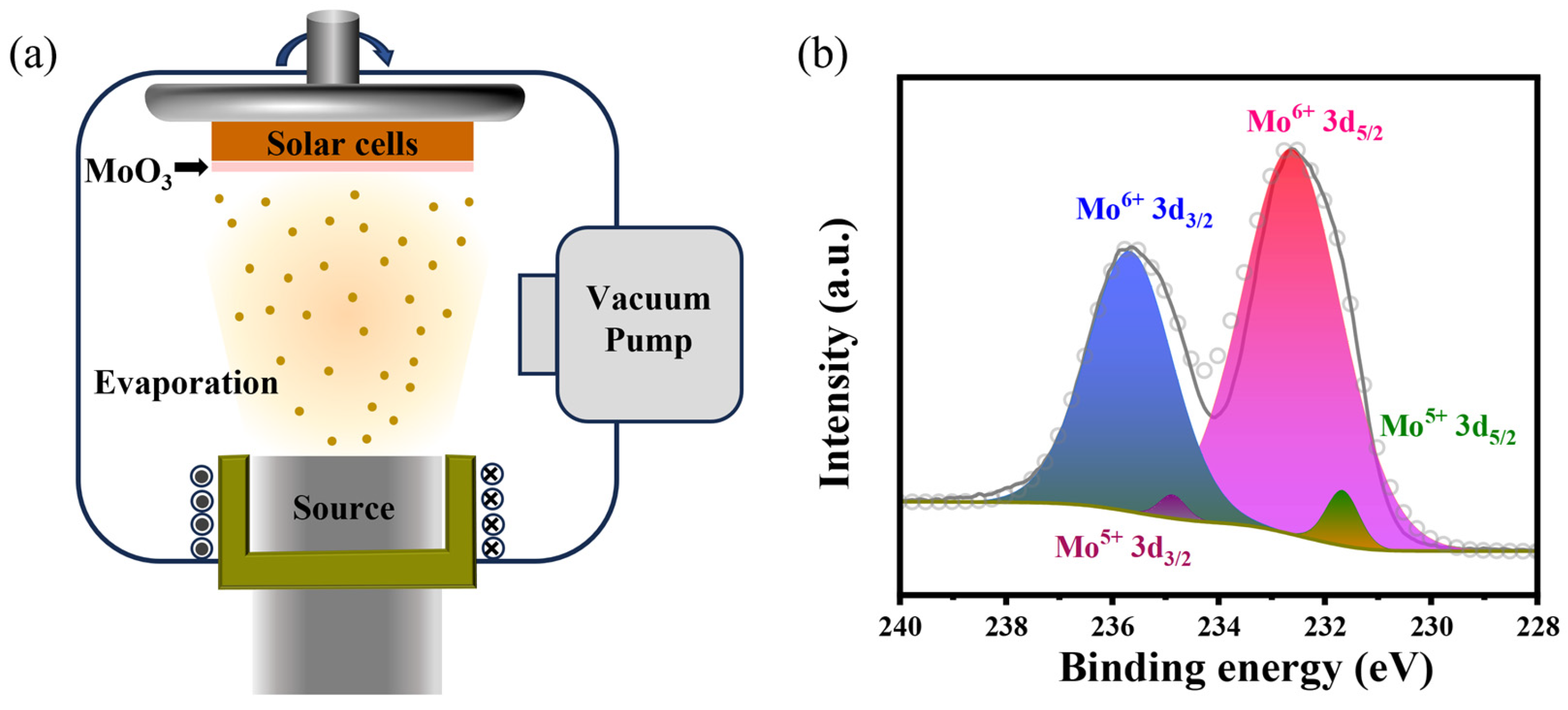
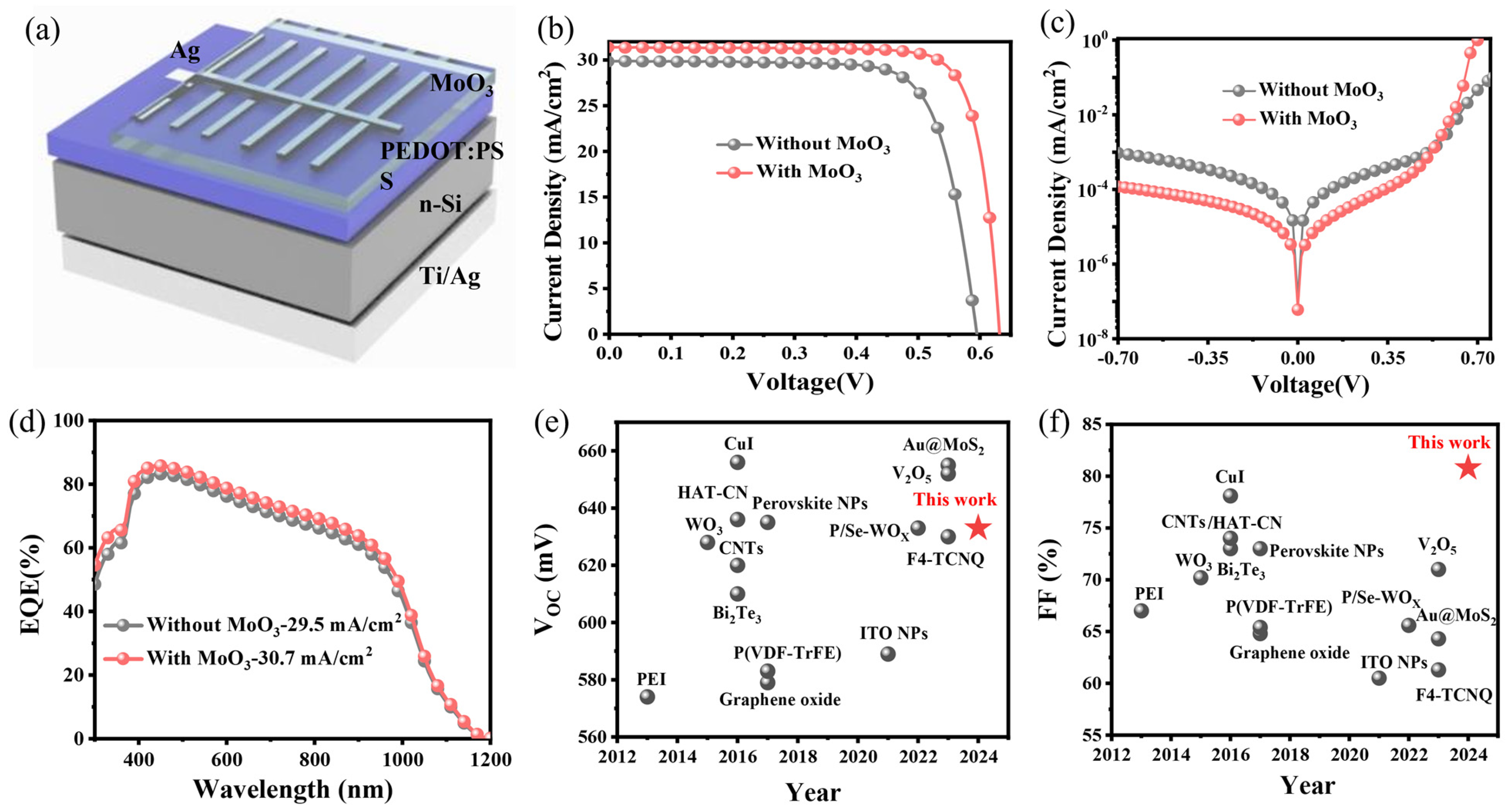
2.1. Device Fabrication

Single-sided polished 100-oriented n-Si wafers (0.1 Ω·cm) with a thickness of 500 μm were utilized for the preparation of PEDOT:PSS/Si solar cells. Before preparing the photovoltaic devices, Si wafers needed to be pre-cleaned using the standard RCA method. The Si substrates were immersed in a diluted HF solution for 10 min to remove natural oxides, after being cleaned. The PEDOT:PSS (Clevios PH1000) solution was mixed with 5 wt% dimethylsulfoxide (DMSO, Sigma-Aldrich, St. Louis, MO, USA) and 1 wt% Triton-X100 (Sigma Aldrich), and then spin-coated on the polished side of the n-Si, which was followed by thermal annealing at 120 °C. A 500 nm thick Ag top grid electrode was subsequently deposited onto the PEDOT:PSS layer through a shadow mask, and a 200/300 nm full-area Ti/Ag film was deposited on the back of the silicon wafer as the rear electrode. Finally, MoO3 films of different thicknesses were deposited on the front surface by thermal evaporation. To avoid any contact issues, the MoO3 film does not cover the region where the probe contacts the Ag electrode. The effective area of each solar cell is 0.5 cm2.

2.2. Device Characterization

The thickness of the MoO3 layers were measured by ellipsometry (M-2000DI). The work function of the samples was determined by ultraviolet photoelectron spectroscopy (UPS). The UPS was performed using a Thermo ESCALAB 250XI (Thermo Fisher, Waltham, MA, USA) at the Shiyanjia Laboratory. The current density–voltage (J-V) characteristics of PEDOT:PSS/Si devices were measured by a solar simulator (Sol3A, Newport, Irvine, CA, USA) under AM 1.5 illumination (1000 W m−2) standard test conditions. The external quantum efficiency (EQE) spectra were measured in the wavelength range 300–1200 nm with the QEX-10 measuring system. Capacitance and voltage measurements were performed using an Agilent B1500A semiconductor parameter analyzer (Agilent, Santa Clara, CA, USA).

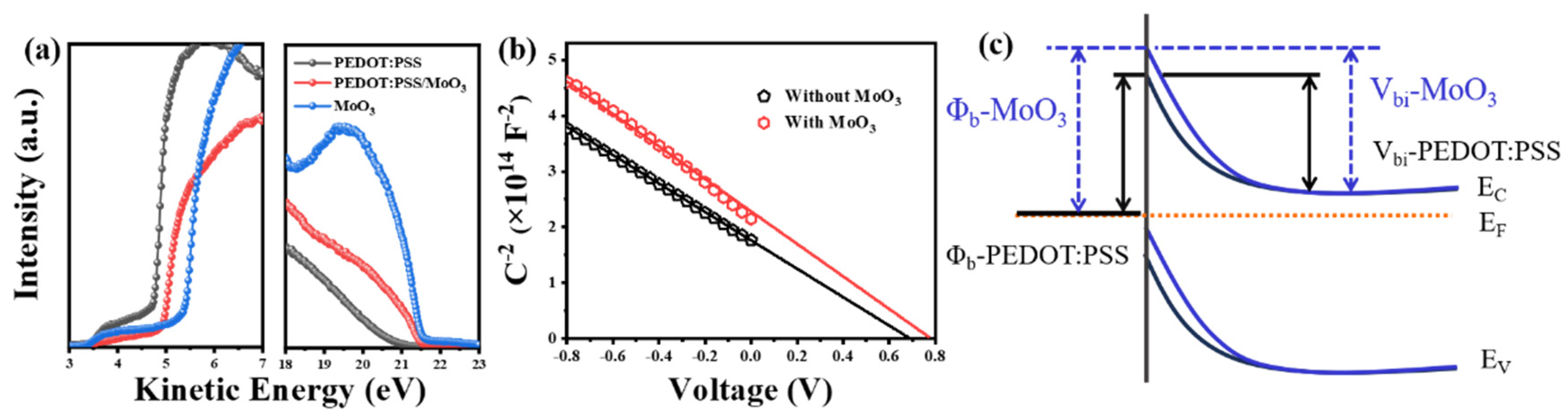
3. Results and Discussion

The thermal evaporation of MoO3 (Figure 1a) shows significant potential for application in photovoltaic devices. X-ray photoelectron spectroscopy (XPS) measurement was conducted on the MoO3 thin films in order to elucidate the composition of the evaporation deposition process. Figure S1 and Figure 1b show the full scan spectra and the XPS spectra of Mo 3d core energy levels for MoO3 thin films, respectively. The Mo 3d doublet shows a 3.05 eV spin–orbit splitting between the Mo 3d3/2 and 3d5/2 bands through simple calculations. In addition, the MoO3 film’s Mo 3d spectra were analyzed using two 3d doublets fitted with a Gaussian function to investigate molybdenum in different oxidation states. The Mo 3d5/2 peak observed at 232.6 eV and the Mo 3d3/2 peak at 235.7 eV suggest the presence of Mo6+, while the Mo 3d5/2 peak at 231.7 eV and the Mo 3d3/2 peak at 234.9 eV are indicative of the existence of Mo5+. Moreover, the calculated experimental value of 0.058 based on the Mo5+/Mo6+ ratio of MoO3 can be utilized to further infer that the stoichiometry of Mo:O is 2.97, indicating that the thermal evaporation-prepared MoO3 thin film possesses an ideal stoichiometric ratio.
Figure 2a shows the schematic representation of the PEDOT:PSS/Si hybrid solar cell, which includes a MoO3 capping layer. We initially deposited MoO3 thin films with varying thicknesses onto the PEDOT:PSS layer and systematically investigated the impact of MoO3 thickness on device performance. The specific results are shown in Figure S2a and summarized in detail in Table S1. As the thickness of MoO3 increases, there are significant increases in VOC, short-circuit current density (JSC), and FF for devices with MoO3 thickness not exceeding 10 nm. However, when the thickness reaches 15 nm, a slight reduction in the photovoltaic parameters of the devices is observed. The impact of MoO3 film thickness on JSC is investigated through the analysis of reflectance spectra, as shown in Figure S2b. It is evident that MoO3 films with a thickness below 15 nm exhibit reduced reflectance across the entire spectral region. When the thickness of MoO3 increases to 30 nm, although the reflectance further decreases in the wavelength range of 600 to 1100 nm, it significantly increases in the ultraviolet wavelength range. Therefore, achieving an optimal thickness of MoO3 is essential for enhancing the JSC of the device. By comparison, it is found that a 10 nm thick MoO3 layer can achieve the optimal photovoltaic performance of the PEDOT:PSS/Si solar cell. Unless otherwise specified, the thickness of MoO3 is 10 nm.
Figure 2b shows the J-V curves of PEDOT:PSS/Si solar cells without and with the MoO3 layer, and the corresponding photovoltaic parameters are summarized in Table 1. The Ag/PEDOT:PSS/n-Si/Ti/Ag structure-based device achieves a PCE of 13.4%, with VOC, JSC, and FF values of 595 mV, 29.8 mA/cm2, and 75.4%, respectively. After being coated with a MoO3 layer, the device exhibits superior performance, with a VOC of 632 mV, a JSC of 31.4 mA/cm2, an FF of 80.8%, and a PCE of 16.0%. For the purpose of comparison, we have provided a summary of the VOC and FF values for Planar Si/PEDOT:PSS solar cells with front interface modification layers, as reported in the literature (Figure 2e,f and Table S2). Compared to other high-performance PEDOT:PSS/Si solar cells, the devices modified with MoO3 have demonstrated superior photovoltaic parameters and performance. It is noteworthy that the FF of the MoO3-based photovoltaic devices in this study represents the highest reported value in PEDOT:PSS/Si solar cells to date.
The improvement of photovoltaic parameters of the device is closely related to the improvement of junction quality. Figure 2c shows the dark J−V characteristics of the PEDOT:PSS/Si solar cells without and with the MoO3 layer. The internal parameters of the device (Table S3) are obtained by fitting the lnI-V curve (Figure S3) and Equation (1).
I = I 0 e x p e v n k T 1 = AA * T 2 e x p b k T e V n k T 1
V O C = k T q l n I S C I 0 + 1
where n is the ideal factor, I is the current value, I0 is the saturation current, V is the applied voltage, q is the electronic charge, A is the contact area (0.5 cm2), T is the absolute temperature (298 K), k is the Boltzmann constant, and A* is the effective Richardson constant (~252 A cm−2 K−2 for n-Si). After conducting calculations, it can be determined that incorporating a MoO3 layer leads to a significant decrease in the n values of PEDOT:PSS/Si devices from 2.39 to 1.66, demonstrating a noticeable enhancement in the quality of the heterojunction. In the absence of a MoO3 layer, the I0 of PEDOT:PSS/Si devices is measured at 2.76 × 10⁻⁷ A, which decreases to 5.75 × 10⁻⁹ A with the introduction of a MoO3 layer. The relationship between VOC and I0 can be described by Equation (2), indicating that the reduction in I0 leads to an increase in the VOC value of the device. The increase in VOC of PEDOT:PSS/Si devices is ascribed to the incorporation of a MoO3 layer, resulting in the augmentation of Vbi near the heterojunction region and improved field-effect passivation, which will be further elucidated later. Additionally, with the incorporation of the MoO3 layer, the barrier height (ΦB) of the device is raised from 0.81 to 0.91 eV. The EQE spectra of devices without and with the MoO3 layer are shown in Figure 2d. The device, which has a layer modified by MoO3, shows an improved optical response in the range of 300 to 1200 nm. This leads to a JSC of 29.5 mA/cm2 for the control solar cells and 30.7 mA/cm2 for the MoO3-modified solar cells, consistent with the results obtained from the J−V curve and photovoltaic parameters.
To elucidate the effect of the MoO3 layer on the interface of PEDOT:PSS/Si heterojunction, the electronic structures of PEDOT:PSS, PEDOT:PSS/MoO3, and MoO3 are determined through UPS measurements (Figure 3a). The work functions of pristine PEDOT:PSS and MoO3 films are 4.8 and 5.4 eV, respectively. When MoO3 is deposited on PEDOT:PSS thin films, the work function of PEDOT:PSS increases by 0.2 eV. The enhanced work function of the PEDOT:PSS film may induce stronger inversion effects, leading to higher Vbi in the Si/PEDOT:PSS heterojunction. The Vbi of the corresponding device can be fitted from the 1/C2-V curve (Figure 3b) and extracted by means of Equation (3).
1 C 2 = 2 ( V b i V ) q ε N d
where Nd is the Si doping level, ε is Si permittivity, and V is applied bias voltage. The Vbi of PEDOT:PSS/Si solar cells with and without the MoO3 layer are 0.78 and 0.68 V, respectively. Fortunately, the introduction of the MoO3 layer significantly increased the Vbi value of the device by 0.1 V. Figure 3c shows the calculated energy band diagram of PEDOT:PSS/Si hybrid solar cells with and without MoO3 capping layer. A large Vbi typically leads to band bending near the Si surface, which is responsible for the increased VOC values in devices with a MoO3 layer.
To further validate the enhanced carrier transfer or separation at the heterojunction interface due to the introduction of the MoO3 layer, we conducted surface-potential measurements of Si/PEDOT:PSS and Si/PEDOT:PSS/MoO3 films in both dark and illuminated conditions using Kelvin probe force microscopy (KPFM), as depicted in Figure 4. The surface potential of the MoO3 layer is enhanced by 40 mV under dark conditions and by 50 mV under irradiation conditions, compared to the original PEDOT:PSS layer. The observed rise in surface potential provides additional evidence for the heightened work function of the PEDOT:PSS layer following its coating with a MoO3 layer. The enhanced work function leads to a more robust built-in electric field, thereby facilitating an increased injection of holes from n-Si into PEDOT:PSS. Furthermore, the significant variation in surface potential difference observed under dark and irradiation conditions can be attributed to the pronounced photoelectric effect that occurs within the n-Si/PEDOT:PSS heterostructure coated with MoO3 when exposed to light.
The introduction of the MoO3 interface layer also provides excellent field-effect passivation at the n-Si/PEDOT:PSS interface, effectively suppressing carrier recombination at the heterojunction interface. To investigate the impact of MoO3 on surface recombination at the PEDOT:PSS/Si heterojunction, minority carrier lifetime (τeff) tests were performed on the relevant sample surfaces using quasi-steady-state photoconductivity (QSSPC) technology (Figure 5a). Figure 5b shows the τeff versus the excess carrier density (Δn) for n-Si substrates passivated by PEDOT:PSS and PEDOT:PSS/MoO3 films. The τeff of an n-type silicon wafer is 3 µs at an injection level of 1014 cm−3. Under the same Δn conditions, the τeff of Si/PEDOT:PSS and Si/PEDOT:PSS/MoO3 samples reaches 157 and 209 µs, respectively. This result indicates that the introduction of a MoO3 layer significantly increases the τeff of the photovoltaic device. There is a close relationship between minority carrier lifetime and surface recombination rate, as shown in Equation (4).
1 τ e f f = 1 τ b u l k + 2 S W
where τbulk is the bulk recombination lifetime, S is the surface recombination rate, and W is the wafer thickness. Due to the use of the same silicon wafer, the τbulk is fixed. Therefore, the surface recombination rate is inversely proportional to the minority carrier lifetime. The introduction of a MoO3 capping layer can be seen to significantly reduce the defect recombination rate at the heterojunction interface, resulting in a higher minority carrier lifetime.

4. Conclusions

In conclusion, a high-work-function MoO3 capping layer was deposited on the PEDOT:PSS side of a solar cell device as a functional layer to modify the band offset near the junction region. Characterization analysis reveals that the introduction of MoO3 thin films significantly increases the Vbi of PEDOT:PSS/Si devices, inducing a strong inversion layer on the Si surface, and significantly improving the VOC and PCE of photovoltaic devices. Therefore, the champion organic/Si solar cell, based on a MoO3 interface layer, exhibits a PCE of 16.0%, with a VOC of 632 mV and an FF as high as 80.8%. This provides a straightforward and promising approach to enhancing the collection and transmission of charge carriers at the interface of photovoltaic devices.

Supplementary Materials

The following supporting information can be downloaded at: https://www.mdpi.com/article/10.3390/nano14201630/s1, Figure S1: Full-scan XPS spectra of thin films composed of MoO3. Figure S2: (a) J-V curves of PEDOT:PSS/Si solar cells with different thicknesses of MoO3 thin layers under simulated AM 1.5 illumination at 100 mW cm−2. (b) Reflectance spectra of polished n-Si and n-Si/PEDOT:PSS/MoO3 surfaces. Figure S3: n and I0 values extrapolated from dln(I) vs. voltage curves. Table S1: The photovoltaic parameters of the hybrid solar cells with different thicknesses of MoO3 thin layers. Table S2: Previous reports on high-performance planar Si/PEDOT:PSS solar cells with a front interface modification layer. Table S3: Summary of n, I0 and ΦB, which is extrapolated from dlnI vs. voltage curves. Refs. [26,27,28,29,30,31,32,33,34,35,36,37,38,39] are cited in the Supplementary Materials.

Author Contributions

Conceptualization, Z.L.; methodology, J.C.; validation, Z.L., J.C. and S.H.; formal analysis, Z.L.; investigation, J.C., Z.L., X.W., Y.L., Y.M., G.L., D.C. and S.H.; resources, Z.L. and S.H.; data curation, J.C. and Z.L.; writing—original draft preparation, Z.L.; writing—review and editing, Z.L.; visualization, J.C. and Z.L.; supervision, Z.L. and S.H.; project administration, Z.L. and S.H.; funding acquisition, Z.L. and S.H. All authors have read and agreed to the published version of the manuscript.

Funding

This work was supported by the Key Research and Development Program of Zhejiang Province (2021C01006) and the National Natural Science Foundation of China (nos. 62404202 and 62341405).

Data Availability Statement

Data are contained within the article and Supplementary Materials.

Conflicts of Interest

The authors declare no conflicts of interest.

References

  1. Lin, H.; Yang, M.; Ru, X.; Wang, G.; Yin, S.; Peng, F.; Hong, C.; Qu, M.; Lu, J.; Fang, L.; et al. Silicon heterojunction solar cells with up to 26.81% efficiency achieved by electrically optimized nanocrystalline-silicon hole contact layers. Nat. Energy 2023, 8, 789–799. [Google Scholar] [CrossRef]
  2. Holman, Z.C.; Descoeudres, A.; Barraud, L.; Fernandez, F.Z.; Seif, J.P.; De Wolf, S.; Ballif, C. Current Losses at the Front of Silicon Heterojunction Solar Cells. IEEE J. Photovolt. 2012, 2, 7–15. [Google Scholar] [CrossRef]
  3. Zhong, S.; Dreon, J.; Jeangros, Q.; Aydin, E.; De Wolf, S.; Fu, F.; Boccard, M.; Ballif, C. Mitigating Plasmonic Absorption Losses at Rear Electrodes in High-Efficiency Silicon Solar Cells Using Dopant-Free Contact Stacks. Adv. Funct. Mater. 2019, 30, 1907840. [Google Scholar] [CrossRef]
  4. Qu, X.; He, Y.; Qu, M.; Ruan, T.; Chu, F.; Zheng, Z.; Ma, Y.; Chen, Y.; Ru, X.; Xu, X.; et al. Identification of embedded nanotwins at c-Si/a-Si:H interface limiting the performance of high-efficiency silicon heterojunction solar cells. Nat. Energy 2021, 6, 194–202. [Google Scholar] [CrossRef]
  5. Yang, X.; Xu, H.; Liu, W.; Bi, Q.; Xu, L.; Kang, J.; Hedhili, M.N.; Sun, B.; Zhang, X.; De Wolf, S. Atomic Layer Deposition of Vanadium Oxide as Hole-Selective Contact for Crystalline Silicon Solar Cells. Adv. Electron. Mater. 2020, 6, 2000467. [Google Scholar] [CrossRef]
  6. Liu, Z.; Lin, W.; Chen, Z.; Chen, D.; Chen, Y.; Shen, H.; Liang, Z. Enhanced Hole Extraction of WOX/V2OX Dopant-Free Contact for p-type Silicon Solar Cell. Adv. Mater. Interfaces 2022, 9, 2102374. [Google Scholar] [CrossRef]
  7. Cao, S.; Li, J.; Zhang, J.; Lin, Y.; Lu, L.; Wang, J.; Yin, M.; Yang, L.; Chen, X.; Li, D. Stable MoOX-Based Heterocontacts for p-Type Crystalline Silicon Solar Cells Achieving 20% Efficiency. Adv. Funct. Mater. 2020, 30, 2004367. [Google Scholar] [CrossRef]
  8. Dréon, J.; Jeangros, Q.; Cattin, J.; Haschke, J.; Antognini, L.; Ballif, C.; Boccard, M. 23.5%-efficient silicon heterojunction silicon solar cell using molybdenum oxide as hole-selective contact. Nano Energy 2020, 70, 104495. [Google Scholar] [CrossRef]
  9. Cao, L.; Procel, P.; Alcañiz, A.; Yan, J.; Tichelaar, F.; Özkol, E.; Zhao, Y.; Han, C.; Yang, G.; Yao, Z.; et al. Achieving 23.83% conversion efficiency in silicon heterojunction solar cell with ultra-thin MoOX hole collector layer via tailoring (i) a-Si:H/MoOX interface. Prog. Photovolt. 2022, 31, 1245–1254. [Google Scholar] [CrossRef]
  10. He, J.; Gao, P.; Yang, Z.; Yu, J.; Yu, W.; Zhang, Y.; Sheng, J.; Ye, J.; Amine, J.C.; Cui, Y. Silicon/Organic Hybrid Solar Cells with 16.2% Efficiency and Improved Stability by Formation of Conformal Heterojunction Coating and Moisture-Resistant Capping Layer. Adv. Mater. 2017, 29, 1606321. [Google Scholar] [CrossRef]
  11. Yoon, S.S.; Khang, D.Y. High Efficiency (>17%) Si-Organic Hybrid Solar Cells by Simultaneous Structural, Electrical, and Interfacial Engineering via Low-Temperature Processes. Adv. Energy Mater. 2017, 8, 1702655. [Google Scholar] [CrossRef]
  12. Shen, R.; Sun, Z.; Shi, Y.; Zhou, Y.; Guo, W.; Zhou, Y.; Yan, H.; Liu, F. Solution Processed Organic/Silicon Nanowires Hybrid Heterojunction Solar Cells Using Organosilane Incorporated Poly (3,4-ethylenedioxythiophene): Poly (styrenesulfonate) as Hole Transport Layers. ACS Nano 2021, 15, 6296–6304. [Google Scholar] [CrossRef] [PubMed]
  13. Wu, S.; Cui, W.; Aghdassi, N.; Song, T.; Duhm, S.; Lee, S.T.; Sun, B. Nanostructured Si/Organic Heterojunction Solar Cells with High Open-Circuit Voltage via Improving Junction Quality. Adv. Funct. Mater. 2016, 26, 5035–5041. [Google Scholar] [CrossRef]
  14. Tong, H.; Yang, Z.; Wang, X.; Liu, Z.; Chen, Z.; Ke, X.; Sui, M.; Tang, J.; Yu, T.; Ge, Z.; et al. Dual Functional Electron-Selective Contacts Based on Silicon Oxide/Magnesium: Tailoring Heterointerface Band Structures while Maintaining Surface Passivation. Adv. Energy Mater. 2018, 8, 1702921. [Google Scholar] [CrossRef]
  15. Lu, Z.; Liu, X.; Hou, G.; Chen, J.; Zhu, T.; Xu, J.; Chen, K. Doping-Free Titanium Nitride Carrier Selective Contacts for Efficient Organic–Inorganic Hybrid Solar Cells. ACS Appl. Energy Mater. 2020, 3, 9208–9215. [Google Scholar] [CrossRef]
  16. Lu, Z.; Hou, G.; Chen, J.; Xu, J.; Chen, K. Achieving a Record Open-Circuit Voltage for Organic/Si Hybrid Solar Cells by Improving Junction Quality. Sol. RRL 2021, 5, 2100255. [Google Scholar] [CrossRef]
  17. Kang, S.B.; Park, W.J.; Jeong, M.H.; Kang, S.H.; Yang, C.; Choi, K.J. Ambipolar Passivated Back Surface Field Layer for Silicon Photovoltaics. Adv. Funct. Mater. 2020, 30, 2004943. [Google Scholar] [CrossRef]
  18. Sheng, J.; Fan, K.; Wang, D.; Han, C.; Fang, J.; Gao, P.; Ye, J. Improvement of the SiOX Passivation Layer for High-Efficiency Si/PEDOT:PSS Heterojunction Solar Cells. ACS Appl. Mater. Interfaces 2014, 6, 16027–16034. [Google Scholar] [CrossRef]
  19. Lee, Y.-T.; Lin, F.-R.; Chen, C.-H.; Pei, Z. A 14.7% Organic/Silicon Nanoholes Hybrid Solar Cell via Interfacial Engineering by Solution-Processed Inorganic Conformal Layer. ACS Appl. Mate. Interfaces 2016, 8, 34537–34545. [Google Scholar] [CrossRef]
  20. Chen, T.-G.; Huang, B.-Y.; Chen, E.-C.; Yu, P.; Meng, H.-F. Micro-textured conductive polymer/silicon heterojunction photovoltaic devices with high efficiency. Appl. Phys. Lett. 2012, 101, 33301. [Google Scholar] [CrossRef]
  21. Mondal, B.K.; Mostaque, S.K.; Rashid, M.A.; Kuddus, A.; Shirai, H.; Hossain, J. Effect of CdS and In3Se4 BSF layers on the photovoltaic performance of PEDOT:PSS/n-Si solar cells: Simulation based on experimental data. Superlattices Microstruct. 2021, 152, 106853. [Google Scholar] [CrossRef]
  22. Cui, Y.; Wei, J.; Xiong, Y.; Shang, Q.-Y.T.; Liu, Q.; Huang, L.; Zhang, Y.; Yu, W. PEDOT: PSS-Nafion/n-Si Hybrid Heterojunction TOPCon Solar Cells: Experiment and Simulation. J. Phys. Chem. C 2024, 128, 2767–2775. [Google Scholar] [CrossRef]
  23. Yu, P.; Tsai, C.-Y.; Chang, J.-K.; Lai, C.-C.; Chen, P.-H.; Lai, Y.-C.; Tsai, P.-T.; Li, M.-C.; Pan, H.-T.; Huang, Y.-Y.; et al. 13% Efficiency Hybrid Organic/Silicon-Nanowire Heterojunction Solar Cell via Interface Engineering. ACS Nano 2013, 7, 10780–10787. [Google Scholar] [CrossRef] [PubMed]
  24. He, J.; Wan, Y.; Gao, P.; Tang, J.; Ye, J. Over 16.7% Efficiency Organic-Silicon Heterojunction Solar Cells with Solution-Processed Dopant-Free Contacts for Both Polarities. Adv. Funct. Mater. 2018, 28, 1802192. [Google Scholar] [CrossRef]
  25. Shen, S.; Zhang, J.; Zhou, S.; Han, Y.; Gao, P.; Sun, B.; Zhao, N.; Wong, C.P. Nanostructured Silicon-Based Heterojunction Solar Cells with Double Hole-Transporting Layers. Adv. Electron. Mater. 2018, 5, 1800070. [Google Scholar] [CrossRef]
  26. Mu, X.; Yu, X.; Xu, D.; Shen, X.; Xia, Z.; He, H.; Zhu, H.; Xie, J.; Sun, B.; Yang, D. High efficiency organic/silicon hybrid solar cells with doping-free selective emitter structure induced by a WO3 thin interlayer. Nano Energy 2015, 16, 54–61. [Google Scholar] [CrossRef]
  27. He, J.; Gao, P.; Ling, Z.; Ding, L.; Yang, Z.; Ye, J.; Cui, Y. High-Efficiency Silicon/Organic Heterojunction Solar Cells with Improved Junction Quality and Interface Passivation. ACS Nano 2016, 10, 11525–11531. [Google Scholar] [CrossRef] [PubMed]
  28. Jiang, X.; Wang, Z.; Han, W.; Liu, Q.; Lu, S.; Wen, Y.; Hou, J.; Huang, F.; Peng, S.; He, D.; et al. High performance silicon–organic hybrid solar cells via improving conductivity of PEDOT:PSS with reduced graphene oxide. Appl. Surf. Sci. 2017, 407, 398–404. [Google Scholar] [CrossRef]
  29. Liu, D.; Zhang, Y.; Fang, X.; Zhang, F.; Song, T.; Sun, B. An 11%-Power-Conversion-Efficiency Organic–Inorganic Hybrid Solar Cell Achieved by Facile Organic Passivation. IEEE Electron Device Lett. 2013, 34, 345–347. [Google Scholar] [CrossRef]
  30. Zhao, Y.; Zhang, L.; Lv, M.; Jiao, C.; Cheng, P.; Fu, Y.; Li, J.; Liu, Q.; He, D. Improvement of the Optoelectrical Properties of a Transparent Conductive Polymer via the Introduction of ITO Nanoparticles and Its Application in Crystalline Silicon/Organic Heterojunction Solar Cells. ACS Appl. Mater. Interfaces 2021, 13, 31171–31179. [Google Scholar] [CrossRef]
  31. Duan, X.; Han, J.; Xia, Z.; Song, T.; Li, Q.; Li, H.; Sun, B. Semiconducting single-walled carbon nanotubes as interfacial modification layers for organic-Si solar cells. Org. Electron. 2016, 28, 205–209. [Google Scholar] [CrossRef]
  32. Kang, S.B.; Jeong, M.H.; Choi, I.Y.; Sohn, S.-D.; Kim, S.H.; Shin, H.-J.; Park, W.I.; Shin, J.C.; Song, M.H.; Choi, K.J. Self-assembled, highly crystalline porous ferroelectric poly(vinylidene fluoride-co-trifluoroethylene) interlayer for Si/organic hybrid solar cells. Nano Energy 2017, 41, 243–250. [Google Scholar] [CrossRef]
  33. Zhao, M.; Zhang, J.; Gao, N.; Song, P.; Bosman, M.; Peng, B.; Sun, B.; Qiu, C.W.; Xu, Q.H.; Bao, Q.; et al. Actively Tunable Visible Surface Plasmons in Bi2Te3 and their Energy-Harvesting Applications. Adv. Mater. 2016, 28, 3138–3144. [Google Scholar] [CrossRef] [PubMed]
  34. Wang, Y.; Xia, Z.; Liu, L.; Xu, W.; Yuan, Z.; Zhang, Y.; Sirringhaus, H.; Lifshitz, Y.; Lee, S.T.; Bao, Q.; et al. The Light-Induced Field-Effect Solar Cell Concept—Perovskite Nanoparticle Coating Introduces Polarization Enhancing Silicon Cell Efficiency. Adv. Mater. 2017, 29, 1606370. [Google Scholar] [CrossRef] [PubMed]
  35. Liu, Y.; Zhang, Z.-g.; Xia, Z.; Zhang, J.; Liu, Y.; Liang, F.; Li, Y.; Song, T.; Yu, X.; Lee, S.-t.; et al. High Performance Nanostructured Silicon–Organic Quasi p–n Junction Solar Cells via Low-Temperature Deposited Hole and Electron Selective Layer. ACS Nano 2015, 10, 704–712. [Google Scholar] [CrossRef]
  36. Ni, Z.; Ding, S.; Zhang, H.; Dai, R.; Chen, A.; Wang, R.; Zhang, J.; Zhou, Y.; Yang, J.; Sun, T.; et al. Phosphorus and Selenium Co-Doped WO3 Nanoparticles for Interface Modification and Photovoltaic Properties Enhancement of Monolayer Planar Silicon/PEDOT:PSS Hybrid Solar Cells. Adv. Mater. Interfaces 2022, 9, 2200812. [Google Scholar] [CrossRef]
  37. Yang, C.; Luo, Z.; Ma, W.; Li, S.; Lv, G.; Fu, K.; Liu, K.; Li, H.; Sun, H.; Chen, X. Study on the Fabrication of PEDOT:PSS/Si Hybrid Solar Cells Incorporated with F4TCNQ and VTMO. J. Phys. Chem. C 2023, 127, 7974–7986. [Google Scholar] [CrossRef]
  38. Wang, J.; Zhou, W.; Wei, Q.; Liu, G.; Yuan, X.; Pen, H.; Zhang, G.; Wang, R.; Wang, C.; Yang, Y. Effect of Au@MoS2 Contacted PEDOT:PSS on Work Function of Planar Silicon Hybrid Solar Cells. Adv. Mater. Interfaces 2023, 10, 2300187. [Google Scholar] [CrossRef]
  39. Luo, Z.; Yang, C.; Chen, X.; Ma, W.; Li, S.; Fu, K. Improving open-circuit voltage and short-circuit current of high-efficiency silicon-based planar heterojunction solar cells by combining V2O5 with PEDOT:PSS. J. Materiomics 2023, 9, 438–446. [Google Scholar] [CrossRef]
Figure 1. (a) Schematic illustration of the thermal evaporation deposition process of the MoO3. (b) The Mo 3d core level of evaporated MoO3 films.
Nanomaterials 14 01630 g001
Figure 2. (a) Device configuration of PEDOT:PSS/Si solar cells with a MoO3 capping layer. (b) J–V curves of PEDOT:PSS/Si solar cells without and with the MoO3 layer under simulated AM 1.5 illumination at 100 mW cm−2. (c) Corresponding dark J−V and (d) EQE curves of PEDOT:PSS/Si solar cells. The historical (e) VOC and (f) FF of high-performance planar Si/PEDOT:PSS solar cells with a modified front interface layer are juxtaposed for comparison.
Nanomaterials 14 01630 g002
Figure 3. (a) UPS measured work function of the as-prepared PEDOT:PSS, PEDOT:PSS/MoO3, and MoO3 films. (b) Capacitance−voltage measurements of the Si/PEDOT:PSS heterojunction solar cells without and with the thin layer of MoO3. (c) Energy band diagram of the PEDOT:PSS/Si hybrid solar cells.
Nanomaterials 14 01630 g003
Figure 4. Surface potential image of MoO3 film partially covering the surface of PEDOT:PSS (a) without and (c) with solar irradiation. Both of the scale bars are 10 µm. Cross-sectional line profile of the surface potential image (b) without and (d) with solar irradiation.
Nanomaterials 14 01630 g004
Figure 5. Characterization of effective carrier lifetime. (a) The schematic of the lifetime measurements using a Sinton Instruments WCT-120 photo-conductance tool and lifetime test structure. (b) The measured effective carrier lifetime as a function of excess carrier density for n-type crystalline silicon wafers symmetrically passivated without and with MoO3 films.
Nanomaterials 14 01630 g005
Table 1. The photovoltaic parameters of the hybrid solar cells with and without the MoO3 layer.
DeviceVOC (mV)Jsc (mA/cm2)FF (%)PCE (%)Rs (Ω·cm2)
w/o MoO359529.875.413.44.5
(593 ± 6)(29.4 ± 0.5)(75.1 ± 0.9)(13.1 ± 0.3)(4.7 ± 0.6)
w/MoO363231.480.816.02.5
(631 ± 2)(30.4 ± 0.5)(80.0 ± 0.4)(15.3 ± 0.4)(2.9 ± 0.3)
Disclaimer/Publisher’s Note: The statements, opinions and data contained in all publications are solely those of the individual author(s) and contributor(s) and not of MDPI and/or the editor(s). MDPI and/or the editor(s) disclaim responsibility for any injury to people or property resulting from any ideas, methods, instructions or products referred to in the content.

