

Photodegradation and van der Waals Passivation of Violet Phosphorus


Abstract
1. Introduction
2. Materials and Methods
2.1. Sample Preparation
2.2. Characterization and Measurement
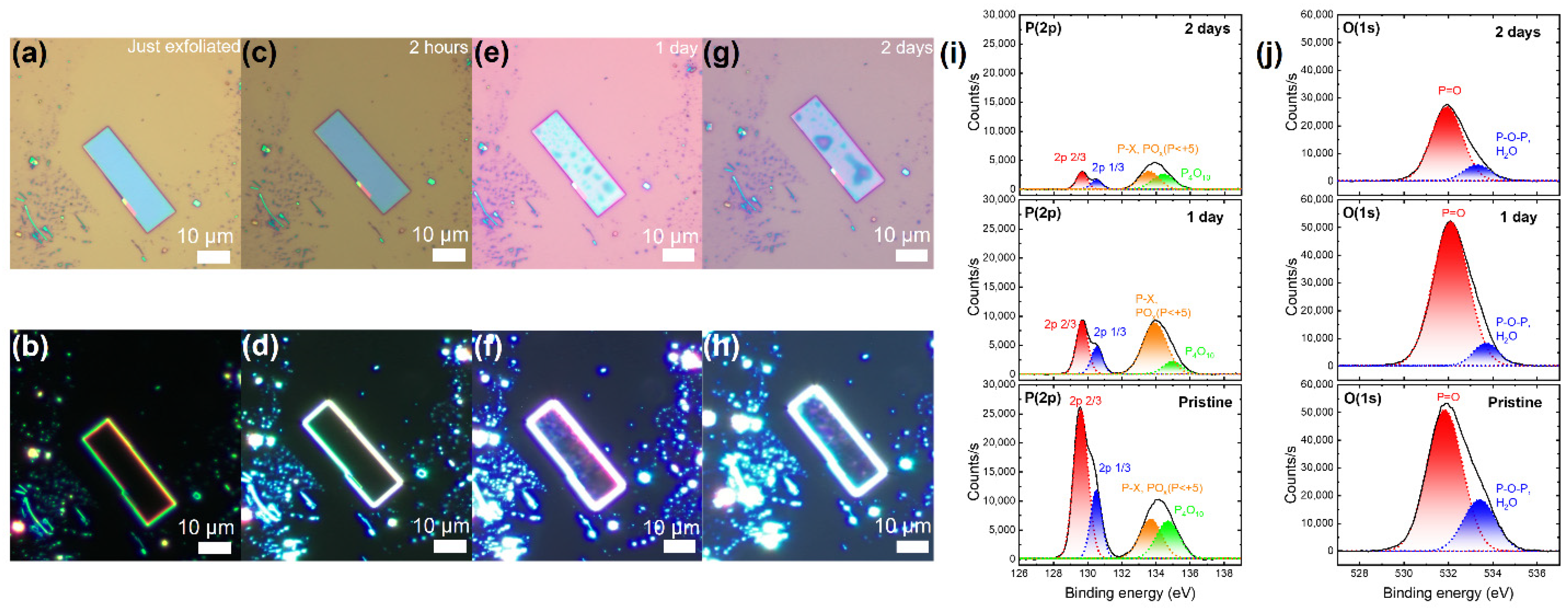
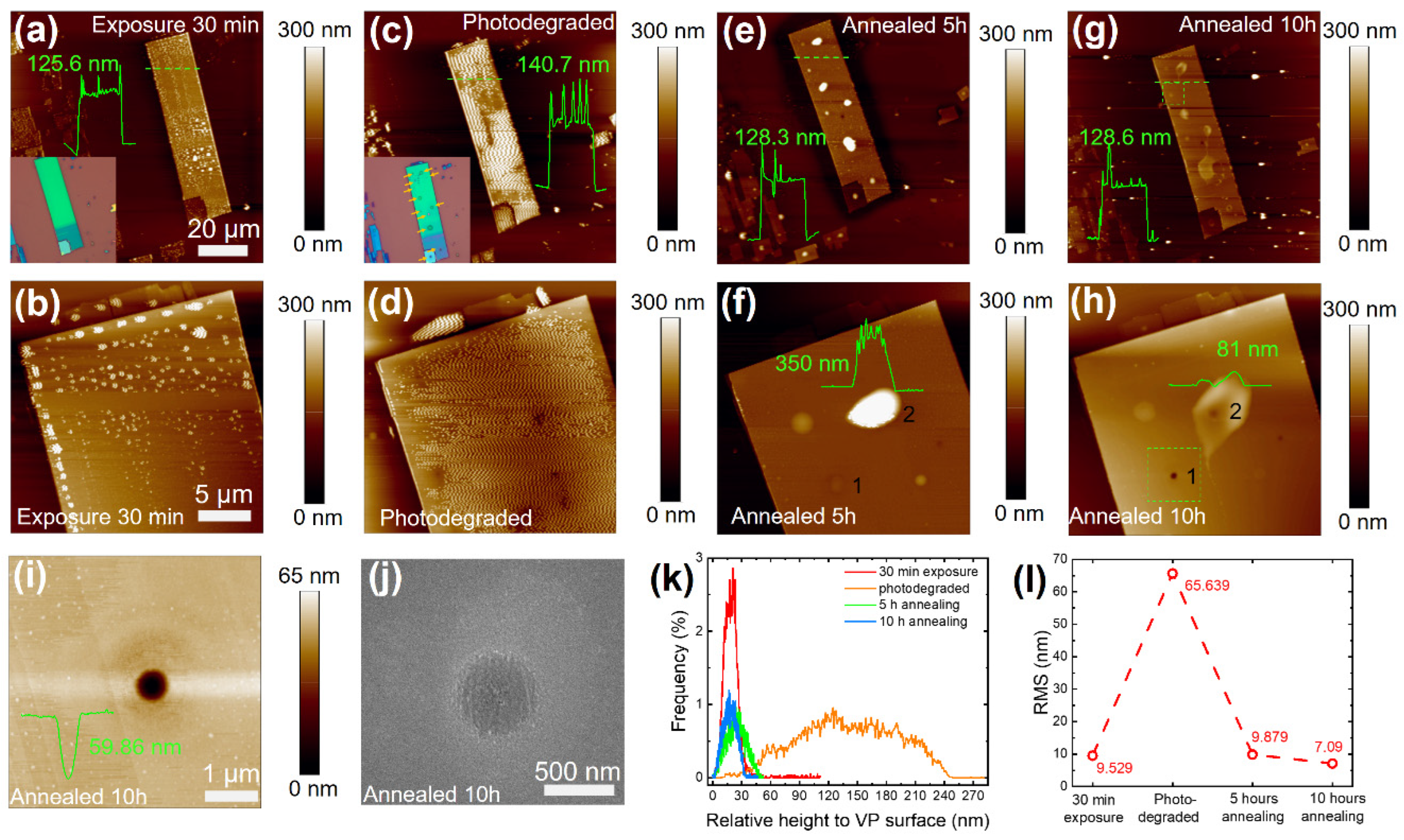
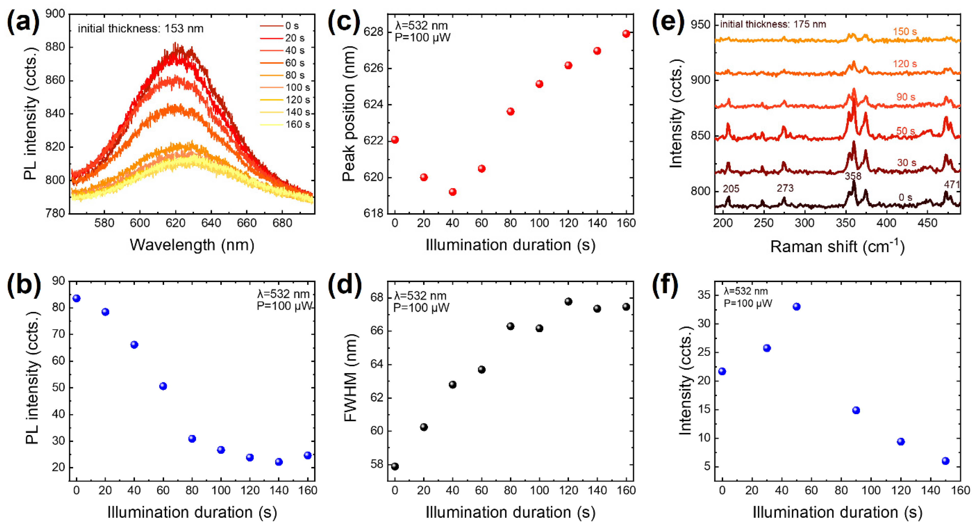
3. Results
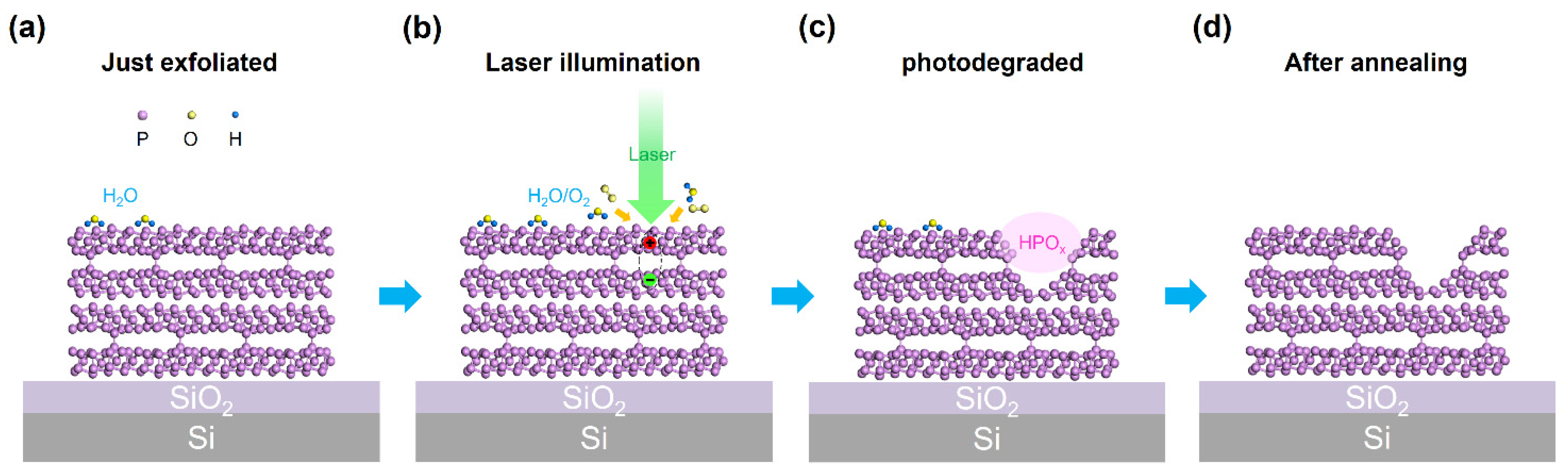
4. Discussion
5. Conclusions
Supplementary Materials
Author Contributions
Funding
Data Availability Statement
Acknowledgments
Conflicts of Interest
References
- Ye, X.; Qi, M.; Chen, M.; Zhang, L.; Zhang, J. Zero to Three Dimension Structure Evolution from Carbon Allotropes to Phosphorus Allotropes. Adv. Mater. Interfaces 2023, 10, 2201941. [Google Scholar] [CrossRef]
- Rabiei Baboukani, A.; Khakpour, I.; Adelowo, E.; Drozd, V.; Shang, W.; Wang, C. High-performance red phosphorus-sulfurized polyacrylonitrile composite by electrostatic spray deposition for lithium-ion batteries. Electrochim. Acta 2020, 345, 136227. [Google Scholar] [CrossRef]
- Liu, Q.; Wang, X.; Zhang, J.; Bian, Y.; Cheng, S.; Kang, Z.; Huang, N.; Gu, H.; Wang, S.; Liu, Y.; et al. Crystalline Red Phosphorus Nanoribbons: Large-Scale Synthesis and Electrochemical Nitrogen Fixation. Angew. Chem. 2020, 59, 14383–14387. [Google Scholar] [CrossRef] [PubMed]
- Liu, L.; Shen, J.; Wu, K.; Yang, N. Two-Dimensional Red Phosphorus Nanosheets: Morphology Tuning and Electrochemical Sensing of Aromatic Amines. Small Methods 2021, 5, 2100720. [Google Scholar] [CrossRef] [PubMed]
- Cicirello, G.; Wang, M.; Sam, Q.P.; Hart, J.L.; Williams, N.L.; Yin, H.; Cha, J.J.; Wang, J. Two-Dimensional Violet Phosphorus P11: A Large Band Gap Phosphorus Allotrope. J. Am. Chem. Soc. 2023, 145, 8218–8230. [Google Scholar] [CrossRef] [PubMed]
- Zhang, L.; Huang, H.; Zhang, B.; Gu, M.; Zhao, D.; Zhao, X.; Li, L.; Zhou, J.; Wu, K.; Cheng, Y.; et al. Structure and Properties of Violet Phosphorus and Its Phosphorene Exfoliation. Angew. Chem. Int. Ed. Engl. 2020, 59, 1074–1080. [Google Scholar] [CrossRef] [PubMed]
- Schusteritsch, G.; Uhrin, M.; Pickard, C.J. Single-Layered Hittorf’s Phosphorus: A Wide-Bandgap High Mobility 2D Material. Nano Lett. 2016, 16, 2975–2980. [Google Scholar] [CrossRef]
- Wang, X.; Jones, A.M.; Seyler, K.L.; Tran, V.; Jia, Y.; Zhao, H.; Wang, H.; Yang, L.; Xu, X.; Xia, F. Highly Anisotropic and Robust Excitons in Monolayer Black Phosphorus. Nat. Nanotechnol. 2015, 10, 517–521. [Google Scholar] [CrossRef]
- Zhang, L.; Li, X.; Yao, F.; Li, L.; Huang, H.; Zhao, X.; Liu, S.; Cheng, Y.; Xu, H.; Zhang, J. Fast Identification of the Crystallographic Orientation of Violet Phosphorus Nanoflakes with Preferred In-Plane Cleavage Edge Orientation. Adv. Funct. Mater. 2022, 32, 2111057. [Google Scholar] [CrossRef]
- Ling, X.; Wang, H.; Huang, S.; Xia, F.; Dresselhaus, M.S. The Renaissance of Black Phosphorus. Proc. Natl. Acad. Sci. USA 2015, 112, 4523. [Google Scholar] [CrossRef]
- Baumer, F.; Ma, Y.; Shen, C.; Zhang, A.; Chen, L.; Liu, Y.; Pfister, D.; Nilges, T.; Zhou, C. Synthesis, Characterization, and Device Application of Antimony-Substituted Violet Phosphorus—A Layered Material. Acs Nano 2017, 11, 4105–4113. [Google Scholar] [CrossRef] [PubMed]
- Li, Y.; Cai, S.; Lai, W.K.; Wang, C.; Rogée, L.; Zhuang, L.; Zhai, L.; Lin, S.; Li, M.; Lau, S.P. Impurity-Induced Robust Trionic Effect in Layered Violet Phosphorus. Adv. Opt. Mater. 2021, 10, 2101538. [Google Scholar] [CrossRef]
- Li, L.; Yu, Y.; Ye, G.J.; Ge, Q.; Ou, X.; Wu, H.; Feng, D.; Chen, X.H.; Zhang, Y. Black phosphorus field-effect transistors. Nat. Nanotechnol. 2014, 9, 372–377. [Google Scholar] [CrossRef] [PubMed]
- Ricciardulli, A.G.; Wang, Y.; Yang, S.; Samori, P. Two-Dimensional Violet Phosphorus: A p-Type Semiconductor for (Opto)electronics. J. Am. Chem. Soc. 2022, 144, 3660–3666. [Google Scholar] [CrossRef] [PubMed]
- Chen, W.; Zhang, R.; Gu, M.; Zhang, L.; Xie, B.; Yu, Z.; Chen, A.; Li, J.; Liu, S.; Gao, P.; et al. An Ultrahigh-Contrast Violet Phosphorus Van der Waals Phototransistor. Adv. Opt. Mater. 2024, 12, 2301399. [Google Scholar] [CrossRef]
- Zhang, X.; Deng, C.; Yu, T.; Yan, X.; Luo, W.; Lv, B.; Liu, J.; Cai, J.; Wei, H.; Li, J.; et al. Ultraclean surface restoration and giant photoresponse enhancement of violet phosphorus. Appl. Surf. Sci. 2024, 651, 159232. [Google Scholar] [CrossRef]
- Liu, X.; Wang, S.; Di, Z.; Wu, H.; Liu, C.; Zhou, P. An Optoelectronic Synapse Based on Two-Dimensional Violet Phosphorus Heterostructure. Adv. Sci. 2023, 10, 2301851. [Google Scholar] [CrossRef]
- Fali, A.; Snure, M.; Abate, Y. Violet phosphorus surface chemical degradation in comparison to black phosphorus. Appl. Phys. Lett. 2021, 118, 163105. [Google Scholar] [CrossRef]
- Doganov, R.A.; O’Farrell, E.C.T.; Koenig, S.P.; Yeo, Y.; Ziletti, A.; Carvalho, A.; Campbell, D.K.; Coker, D.F.; Watanabe, K.; Taniguchi, T. Transport properties of pristine few-layer black phosphorus by van der Waals passivation in an inert atmosphere. Nat. Commun. 2015, 6, 6647. [Google Scholar] [CrossRef]
- Ziletti, A.; Carvalho, A.; Trevisanutto, P.E.; Campbell, D.K.; Coker, D.F.; Neto, A.H.C. Phosphorene oxides: Bandgap engineering of phosphorene by oxidation. Phys. Rev. 2015, 91, 085407. [Google Scholar] [CrossRef]
- Lin, S.; Lai, W.K.; Li, Y.; Lu, W.; Lau, S.P. Liquid-phase exfoliation of violet phosphorus for electronic applications. SmartMat 2021, 2, 226–233. [Google Scholar] [CrossRef]
- Baboukani, A.R.; Aghaei, S.M.; Khakpour, I.; Drozd, V.; Aasi, A.; Wang, C. Defects investigation of bipolar exfoliated phosphorene nanosheets. Surf. Sci. 2022, 720, 122052. [Google Scholar] [CrossRef]
- Favron, A.; Gaufres, E.; Fossard, F.; Phaneuf-L’Heureux, A.L.; Tang, N.Y.W.; Levesque, P.L.; Loiseau, A.; Leonelli, R.; Francoeur, S.; Martel, R. Photooxidation and quantum confinement effects in exfoliated black phosphorus. Nat. Mater. 2015, 14, 826–832. [Google Scholar] [CrossRef] [PubMed]
- Kim, J.S.; Liu, Y.; Zhu, W.; Kim, S.; Wu, D.; Tao, L.; Dodabalapur, A.; Lai, K.; Akinwande, D. Toward air-stable multilayer phosphorene thin-films and transistors. Sci. Rep. 2015, 5, 8989. [Google Scholar] [CrossRef] [PubMed]
- Plasma-Treated Thickness-Controlled Two-Dimensional Black Phosphorus and Its Electronic Transport Properties. Acs Nano 2015, 9, 8729–8736. [CrossRef] [PubMed]
- Island, J.O.; Steele, G.A.; Zant, H.S.J.V.D.; Castellanos-Gomez, A. Environmental instability of few-layer black phosphorus. 2D Mater. 2014, 2, 011002. [Google Scholar] [CrossRef]
- Castellanos-Gomez, A.; Vicarelli, L.; Prada, E.; Island, J.O.; Narasimha-Acharya, K.L.; Blanter, S.I.; Groenendijk, D.J.; Buscema, M.; Steele, G.A.; Alvarez, J.V. Isolation and characterization of few-layer black phosphorus. 2D Mater. 2014, 1, 025001. [Google Scholar] [CrossRef]
- Ghafariasl, M.; Singh, S.; Gamage, S.; Prusnick, T.; Snure, M.; Abate, Y. Photodegradation and Thermal Effects in Violet Phosphorus. Adv. Mater. Interfaces 2024, 2300794. [Google Scholar] [CrossRef]
- Wood, J.D.; Wells, S.A.; Jariwala, D.; Chen, K.-S.; Cho, E.; Sangwan, V.K.; Liu, X.; Lauhon, L.J.; Marks, T.J.; Hersam, M.C. Effective Passivation of Exfoliated Black Phosphorus Transistors against Ambient Degradation. Nano Lett. 2014, 14, 6964–6970. [Google Scholar] [CrossRef]
- Brunner, J.; Thüler, M.; Veprek, S.; Wild, R. X-ray photoelectron study of amorphous phosphorus preparedbyplasmachemical transport. Comparison with crystalline polymorphs. J. Phys. Chem. Solids 1979, 40, 967–971. [Google Scholar] [CrossRef]
- Harada, Y.; Murano, K.; Shirotani, I.; Takahashi, T.; Maruyama, Y. Electronic structure of black phosphorus studied by X-ray photoelectron spectroscopy. Solid. State Commun. 1982, 44, 877–879. [Google Scholar] [CrossRef]
- ThØGersen, A.; Syre, M.; Retterstol Olaisen, B.; Diplas, S. Studies of the oxidation states of phosphorus gettered silicon substrates using X-ray photoelectron spectroscopy and transmission electron microscopy. J. Appl. Phys. 2013, 113, 044307. [Google Scholar] [CrossRef]
- Zhu, H.; Mcdonnell, S.; Qin, X.; Azcatl, A.; Cheng, L.; Addou, R.; Kim, J.; Ye, P.D.; Wallace, R.M. Al2O3 on Black Phosphorus by Atomic Layer Deposition: An in Situ Interface Study. ACS Appl. Mater. Interfaces 2015, 7, 13038–13043. [Google Scholar] [CrossRef] [PubMed]
- Kwon, H.; Seo, S.W.; Kim, T.G.; Lee, E.S.; Kim, J.W. Ultrathin and Flat Layer Black Phosphorus Fabricated by Reactive Oxygen and Water Rinse. Acs Nano 2016, 10, 8723. [Google Scholar] [CrossRef] [PubMed]
- Verdaguer, A.; Weis, C.; Oncins, G.; Ketteler, G.; Bluhm, H. Growth and structure of water on SiO2 films on Si Investigated by Kelvin probe microscopy and in Situ X-ray spectroscopies. Langmuir 2007, 23, 9699–9703. [Google Scholar] [CrossRef] [PubMed]
- Mao, Z.; Dong, S.; Li, J.; Lin, X.; Jian, X.; Wu, P. Hittorf’s violet phosphorene as a promising candidate for NO2, O3 and SO2 sensor: A first-principles investigation. Solid. State Commun. 2020, 314, 113928. [Google Scholar] [CrossRef]
- Zhang, X.; Yang, H.; Hou, W.; Zheng, X.; Qin, S. Twist-angle modulation of exciton absorption in MoS2/graphene heterojunctions. Appl. Phys. Lett. 2019, 115, 181901. [Google Scholar] [CrossRef]
- Lee, C.; Yan, H.; Brus, L.E.; Heinz, T.F.; Hone, J.; Ryu, S. Anomalous Lattice Vibrations of Single- and Few-Layer MoS2. ACS Nano 2010, 4, 2695–2700. [Google Scholar] [CrossRef]
- Splendiani, A.; Sun, L.; Zhang, Y.; Li, T.; Kim, J.; Chim, C.-Y.; Galli, G.; Wang, F. Emerging Photoluminescence in Monolayer MoS2. Nano Lett. 2010, 10, 1271–1275. [Google Scholar] [CrossRef]
- Ellis, J.K.; Lucero, M.J.; Scuseria, G.E. The indirect to direct band gap transition in multilayered MoS2 as predicted by screened hybrid density functional theory. Appl. Phys. Lett. 2011, 99, 261908. [Google Scholar] [CrossRef]
- Mak, K.F.; He, K.; Lee, C.; Lee, G.H.; Hone, J.; Heinz, T.F.; Shan, J. Tightly bound trions in monolayer MoS2. Nat. Mater. 2013, 12, 207–211. [Google Scholar] [CrossRef] [PubMed]
- Mouri, S.; Miyauchi, Y.; Matsuda, K. Tunable Photoluminescence of Monolayer MoS2 via Chemical Doping. Nano Lett. 2013, 13, 5944–5948. [Google Scholar] [CrossRef] [PubMed]
- Tonndorf, P.; Schmidt, R.; Böttger, P.; Zhang, X.; Börner, J.; Liebig, A.; Albrecht, M.; Kloc, C.; Gordan, O.; Zahn, D.R.; et al. Photoluminescence emission and Raman response of monolayer MoS2, MoSe2, and WSe2. Opt. Express 2013, 21, 4908–4916. [Google Scholar] [CrossRef] [PubMed]
- Eckmann, A.; Felten, A.; Verzhbitskiy, I.; Davey, R.; Casiraghi, C. Raman study on defective graphene: Effect of the excitation energy, type, and amount of defects. Phys. Rev. B. Condens. Matter Mater. Phys. 2013, 88, 035426. [Google Scholar] [CrossRef]
- Zhang, L.; Huang, H.; Lv, Z.; Li, L.; Gu, M.; Zhao, X.; Zhang, B.; Cheng, Y.; Zhang, J. Phonon Properties of Bulk Violet Phosphorus Single Crystals: Temperature and Pressure Evolution. ACS Appl. Electron. Mater. 2021, 3, 1043–1049. [Google Scholar] [CrossRef]
- ZnO nanowire UV photodetectors with high internal gain. Nano Lett. 2007, 7, 1003–1009. [CrossRef] [PubMed]
- Li, Q.H.; Gao, T.; Wang, Y.G.; Wang, T.H. Adsorption and desorption of oxygen probed from ZnO nanowire films by photocurrent measurements. Appl. Phys. Lett. 2005, 86, 509. [Google Scholar] [CrossRef]
- Takahashi, Y.; Kanamori, M.; Kondoh, A.; Minoura, H.; Ohya, Y. Photoconductivity of Ultrathin Zinc Oxide Films. Jpn. J. Appl. Phys. 1994, 33, 6611–6615. [Google Scholar] [CrossRef]
- Wang, H.; Wu, Y.; Cong, C.; Shang, J.; Yu, T. Hysteresis of Electronic Transport in Graphene Transistors. ACS Nano 2010, 4, 7221–7228. [Google Scholar] [CrossRef]
- Yang, H.; Tan, C.; Deng, C.; Zhang, R.; Zheng, X.; Zhang, X.; Hu, Y.; Guo, X.; Wang, G.; Jiang, T.; et al. Photodetectors: Bolometric Effect in Bi2O2Se Photodetectors (Small 43/2019). Small 2019, 15, 1970235. [Google Scholar] [CrossRef]
- Koppens, F.H.; Mueller, T.; Avouris, P.; Ferrari, A.C.; Vitiello, M.S.; Polini, M. Photodetectors based on graphene, other two-dimensional materials and hybrid systems. Nat. Nanotechnol. 2014, 9, 780–793. [Google Scholar] [CrossRef]
- Wu, J.; Koon, G.K.W.; Xiang, D.; Han, C.; Toh, C.T.; Kulkarni, E.S.; Verzhbitskiy, I.; Carvalho, A.; Rodin, A.S.; Koenig, S.P.; et al. Colossal Ultraviolet Photoresponsivity of Few-Layer Black Phosphorus. ACS Nano 2015, 9, 8070–8077. [Google Scholar] [CrossRef]
- Yau, S.L.; Moffat, T.P.; Bard, A.J.; Zhang, Z.; Lerner, M.M. STM of the (010) surface of orthorhombic phosphorus. Chem. Phys. Lett. 1992, 198, 383–388. [Google Scholar] [CrossRef]
- Nan, H.; Wang, Z.; Wang, W.; Liang, Z.; Lu, Y.; Chen, Q.; He, D.; Tan, P.; Miao, F.; Wang, X. Strong Photoluminescence Enhancement of MoS2 through Defect Engineering and Oxygen Bonding. ACS Nano 2014, 8, 5738–5745. [Google Scholar] [CrossRef]

Disclaimer/Publisher’s Note: The statements, opinions and data contained in all publications are solely those of the individual author(s) and contributor(s) and not of MDPI and/or the editor(s). MDPI and/or the editor(s) disclaim responsibility for any injury to people or property resulting from any ideas, methods, instructions or products referred to in the content. |
© 2024 by the authors. Licensee MDPI, Basel, Switzerland. This article is an open access article distributed under the terms and conditions of the Creative Commons Attribution (CC BY) license (https://creativecommons.org/licenses/by/4.0/).
Share and Cite
Zhang, X.; Lv, B.; Wei, H.; Yan, X.; Peng, G.; Qin, S. Photodegradation and van der Waals Passivation of Violet Phosphorus. Nanomaterials 2024, 14, 422. https://doi.org/10.3390/nano14050422
Zhang X, Lv B, Wei H, Yan X, Peng G, Qin S. Photodegradation and van der Waals Passivation of Violet Phosphorus. Nanomaterials. 2024; 14(5):422. https://doi.org/10.3390/nano14050422
Chicago/Turabian StyleZhang, Xiangzhe, Bowen Lv, Haitao Wei, Xingheng Yan, Gang Peng, and Shiqiao Qin. 2024. "Photodegradation and van der Waals Passivation of Violet Phosphorus" Nanomaterials 14, no. 5: 422. https://doi.org/10.3390/nano14050422
APA StyleZhang, X., Lv, B., Wei, H., Yan, X., Peng, G., & Qin, S. (2024). Photodegradation and van der Waals Passivation of Violet Phosphorus. Nanomaterials, 14(5), 422. https://doi.org/10.3390/nano14050422