
Structure–Piezoelectric Property Relationships of Thin Films Composed of Electrospun Aligned Poly(vinylidene fluoride) Nanofibers
 ,
,
Abstract
:1. Introduction
2. Materials and Methods
2.1. Materials
2.2. Preparation of Nanofibers
2.3. Hot-Pressing and Poling
2.4. Characterization
3. Results and Discussion
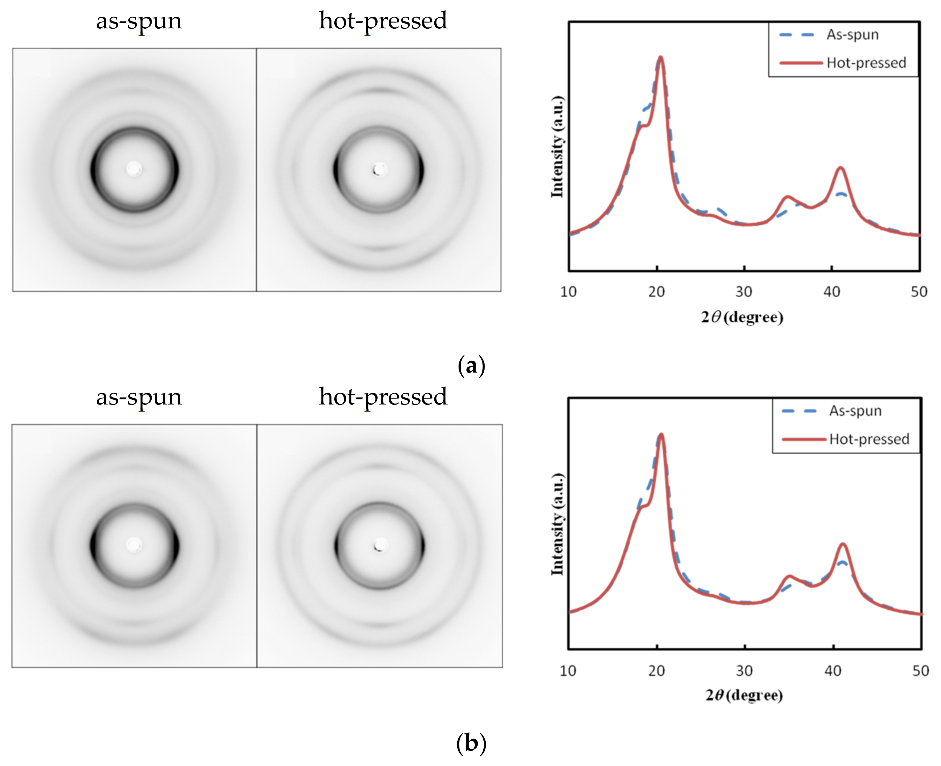
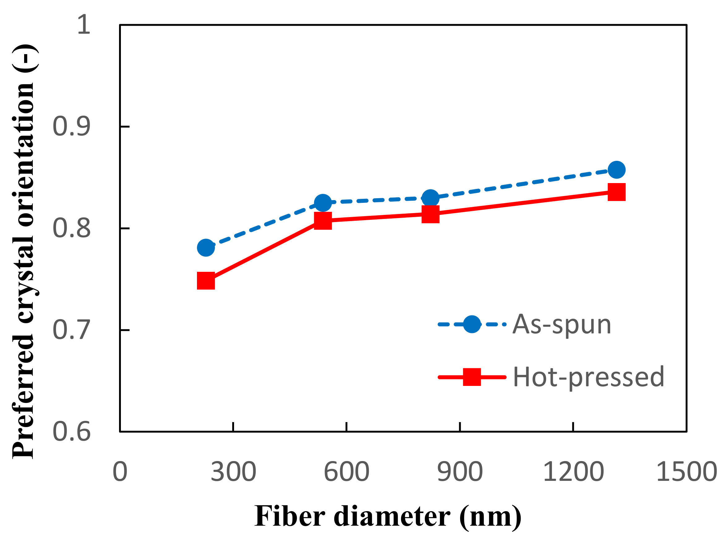
3.1. Preparation and Characterization of Aligned PVDF Nanofibers
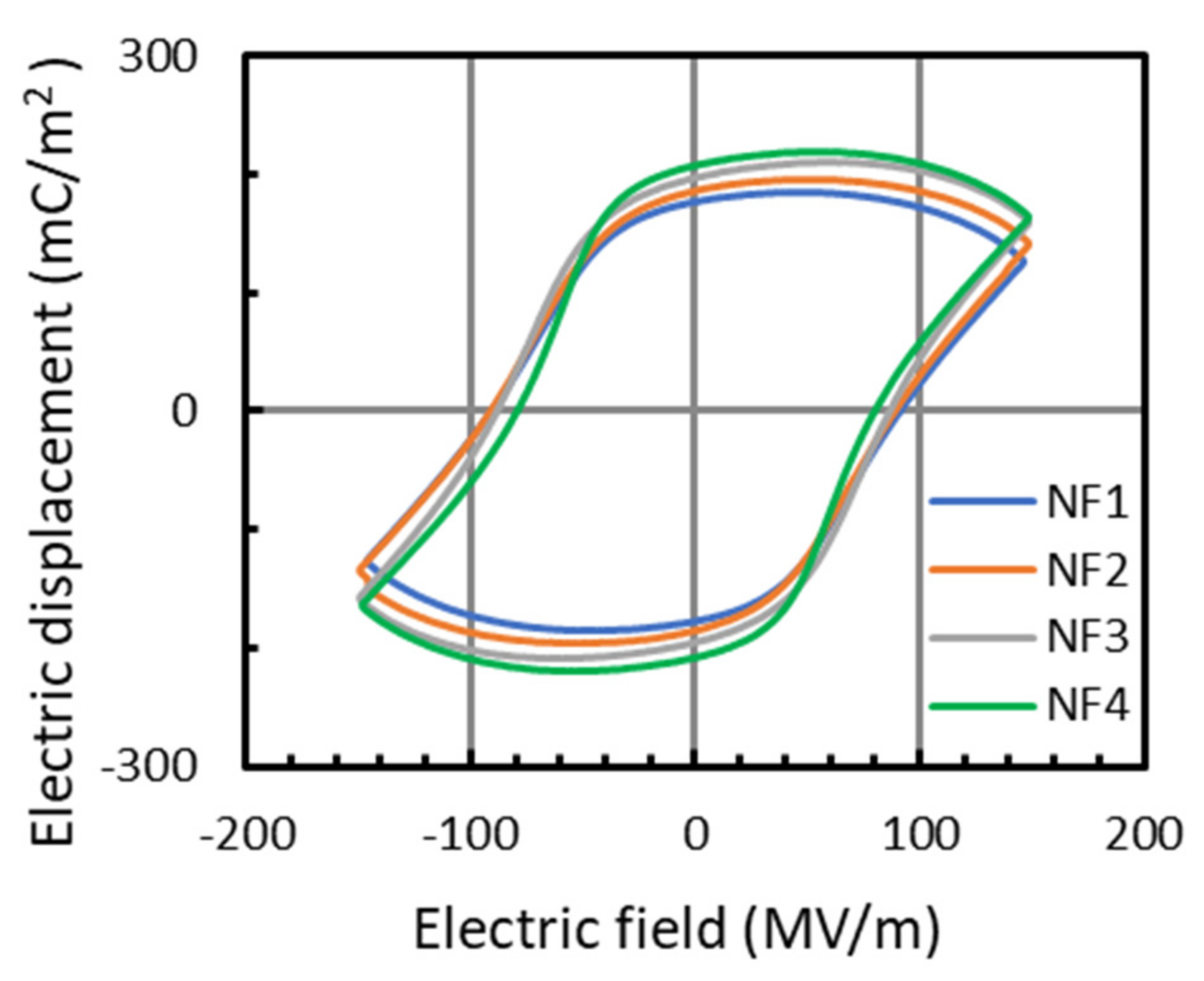
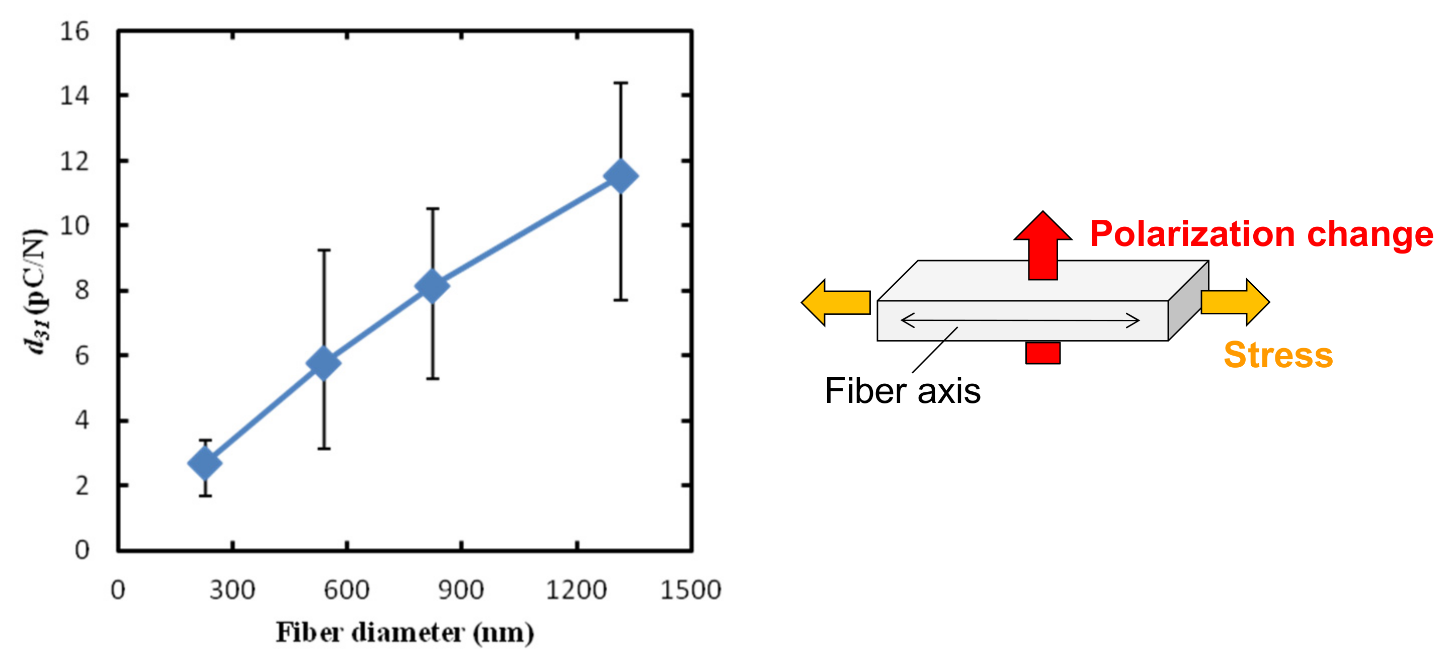
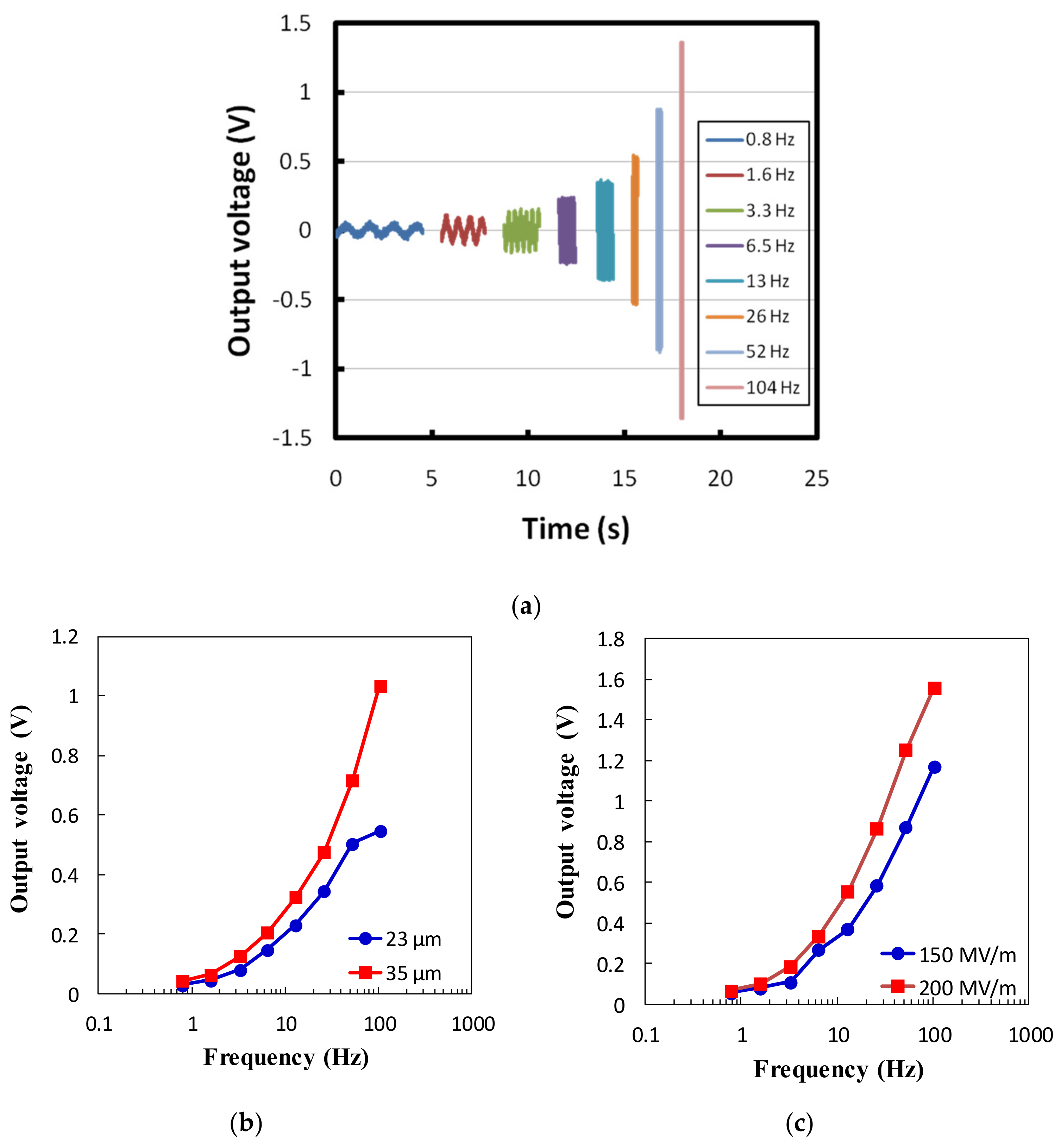
3.2. Piezoelectric Properties of PVDF Nanofiber Thin Films
4. Conclusions
Supplementary Materials
Author Contributions
Funding
Data Availability Statement
Acknowledgments
Conflicts of Interest
References
- Zi, Y.; Wang, Z.L. Nanogenerators: An emerging technology towards nanoenergy. APL Mater. 2017, 5, 074103. [Google Scholar] [CrossRef]
- Wan, X.; Cong, H.; Jiang, G.; Liang, X.; Liu, L.; He, H. A review on PVDF nanofibers in textiles for flexible piezoelectric sensors. ACS Appl. Nano Mater. 2023, 6, 1522–1540. [Google Scholar] [CrossRef]
- Kenry; Lim, C.T. Nanofiber Technology: Current status and emerging developments. Prog. Polym. Sci. 2017, 70, 1–17. [Google Scholar] [CrossRef]
- Kawai, H. The piezoelectricity of poly(vinylidene fluoride). Jpn. J. Appl. Phys. 1969, 8, 975. [Google Scholar] [CrossRef]
- Pan, X.; Wang, Z.; Cao, Z.; Zhang, S.; He, Y.; Zhang, Y.; Chen, K.; Hu, Y.; Gu, H. A self-powered vibration sensor based on electrospun poly(vinylidene fluoride) nanofibres with enhanced piezoelectric response. Smart Mater. Struct. 2016, 25, 105010. [Google Scholar] [CrossRef]
- Lolla, D.; Gorse, J.; Kisielowski, C.; Miao, J.; Taylor, P.L.; Chase, G.G.; Reneker, D.H. Polyvinylidene fluoride molecules in nanofibers, imaged at atomic scale by aberration corrected electron microscopy. Nanoscale 2016, 8, 120–128. [Google Scholar] [CrossRef]
- Nasir, M.; Matsumoto, H.; Minagawa, M.; Tanioka, A.; Danno, T.; Horibe, H. Formation of β-phase crystalline structure of PVDF nanofiber by electrospray deposition: Additive effect of ionic fluorinated surfactant. Polym. J. 2007, 39, 670–674. [Google Scholar] [CrossRef]
- Danno, T.; Matsumoto, H.; Nasir, M.; Shimizu, S.; Minagawa, M.; Kawaguchi, J.; Horibe, H.; Tanioka, A. Fine structure of PVDF nanofiber fabricated by electrospray deposition. J. Polym. Sci. B Polym. Phys. 2008, 46, 558–563. [Google Scholar] [CrossRef]
- Yarin, A.L.; Pourdeyhimi, B.; Ramakrishna, S. Fundamentals and Applications of Micro- and Nanofibers; Cambridge University Press: Cambridge, UK, 2014. [Google Scholar]
- Uematsu, I.; Uchida, K.; Nakagawa, Y.; Matsumoto, H. Direct observation and quantitative analysis of the fiber formation process during electrospinning by a high-speed camera. Ind. Eng. Chem. Res. 2018, 57, 12122–12126. [Google Scholar] [CrossRef]
- Chen, X.; Tougne, C.; Jiang, T.; Espindola-Rodriguez, M.; Zhao, Q.; Jia, Q.; Mendil-Jakani, H.; Jiang, J.; Zhang, W. Highly oriented PVDF molecular chains for enhanced material performance. Polymer 2022, 261, 125366. [Google Scholar] [CrossRef]
- Farrar, D.; Ren, K.; Cheng, D.; Kim, S.; Moon, W.; Wilson, W.L.; West, J.E.; Yu, S.M. Permanent polarity and piezoelectricity of electrospun α-helical poly(α-amino acid) fibers. Adv. Mater. 2011, 23, 3954–3958. [Google Scholar] [CrossRef]
- Anwar, S.; Amiri, M.H.; Jiang, S.; Abolhasani, M.M.; Rocha, P.R.F.; Asadi, K. Piezoelectric nylon-11 fibers for electronic textiles, energy harvesting and sensing. Adv. Funct. Mater. 2021, 31, 2004326. [Google Scholar] [CrossRef]
- Yang, Z.; Takarada, W.; Matsumoto, H. Effect of the fiber diameter of polyamide 11 nanofibers on their internal molecular orientation and properties. Macromol. Rapid Commun. 2023, 44, 2300212. [Google Scholar] [CrossRef] [PubMed]
- Azzaz, C.M.; Mattoso, L.H.C.; Demarquette, N.R.; Zednik, R.J. Polyvinylidene fluoride nanofibers obtained by electrospinning and blowspinning: Electrospinning enhances the piezoelectric β-phase—Myth or reality? J. Appl. Polym. Sci. 2021, 138, e49959. [Google Scholar] [CrossRef]
- Chang, C.; Tran, V.H.; Wang, J.; Fuh, Y.-K.; Lin, L. Direct-write piezoelectric polymeric nanogenerator with high energy conversion efficiency. Nano Lett. 2010, 10, 726–731. [Google Scholar] [CrossRef]
- Pu, J.; Yan, X.; Jiang, Y.; Chang, C.; Lin, L. Flexible piezoelectric transducer based on electrospun PVDF nanofibers for sensing applications. Sens. Act. A 2010, 164, 131–136. [Google Scholar] [CrossRef]
- Fang, J.; Wang, X.; Lin, T. Electrical power generator from randomly oriented electrospun poly(vinylidene fluoride) nanofibre membranes. J. Mater. Chem. 2011, 21, 11088–11091. [Google Scholar] [CrossRef]
- Shao, H.; Fang, J.; Wang, H.; Lin, T. Effect of electrospinning parameters and polymer concentrations on mechanical-to-electrical energy conversion of randomly-oriented electrospun poly(vinylidene fluoride) nanofiber mats. RSC Adv. 2015, 5, 14345–14350. [Google Scholar] [CrossRef]
- Shao, H.; Fang, J.; Wang, H.; Lang, C.; Yan, G.; Lin, T. Mechanical energy-to-electricity conversion of electron/hole-transfer agent-doped poly(vinylidene fluoride) nanofiber webs. Macromol. Mater. Eng. 2017, 302, 1600451. [Google Scholar] [CrossRef]
- Yin, J.-Y.; Boaretti, C.; Lorenzetti, A.; Martucci, A.; Roso, M.; Modesti, M. Effects of solvent and electrospinning parameters on the morphology and piezoelectric properties of PVDF nanofibrous membrane. Nanomaterials 2022, 12, 962. [Google Scholar] [CrossRef]
- Wang, S.; Tang, C.-Y.; Jia, J.; Zha, X.-J.; Liu, J.-H.; Zhao, X.; Ke, K.; Wang, Y.; Yang, W. Liquid electrolyte-assisted electrospinning for boosting piezoelectricity of poly(vinylidene fluoride) fiber mats. Macromolecules 2023, 56, 7479–7489. [Google Scholar] [CrossRef]
- Persano, L.; Dagdeviren, C.; Su, Y.; Zhang, Y.; Girardo, S.; Pisignano, D.; Huang, Y.; Rogers, J.A. High performance piezoelectric devices based on aligned arrays of nanofibers of poly(vinylidenefluoride-co-trifluoroethylene). Nat. Commun. 2013, 4, 1633. [Google Scholar] [CrossRef]
- Zhang, S.; Zhang, B.; Zhang, J.; Ren, K. Enhanced piezoelectric performance of various electrospun PVDF nanofibers and related self-powered device applications. ACS Appl. Mater. Interfaces 2021, 13, 32242–32250. [Google Scholar] [CrossRef] [PubMed]
- Mane, S.; Teli, A.; Deonikar, V.; Patil, D.; Shin, J.C. Hydrothermally prepared nano bricks of potassium sodium niobate for enhancing thermal and electrical properties of poly(vinylidene fluoride). Mater. Lett. 2023, 338, 134040. [Google Scholar] [CrossRef]
- He, Z.; Rault, F.; Lewandowski, M.; Mohsenzadeh, E.; Salaün, F. Electrospun PVDF nanofibers for piezoelectric applications: A review of the influence of electrospinning parameters on the phase and crystallinity enhancement. Polymers 2021, 13, 174. [Google Scholar] [CrossRef] [PubMed]
- Liu, X.; Xu, S.; Kuang, X.; Tan, D.; Wang, X. Nanoscale investigations on β-phase orientation, piezoelectric response, and polarization direction of electrospun PVDF nanofibers. RSC Adv. 2016, 6, 109061–109066. [Google Scholar] [CrossRef]
- Liu, X.; Deng, M.; Wang, X. Nanoscale domain imaging and local piezoelectric coefficient d33 studies of single piezoelectric polymeric nanofibers. Mater. Lett. 2017, 189, 66–69. [Google Scholar] [CrossRef]
- Feng, Z.; Zhao, Z.; Liu, Y.; Liu, Y.; Cao, X.; Yu, D.-G.; Wang, K. Piezoelectric effect polyvinylidene fluoride (PVDF): From energy harvester to smart skin and electronic textiles. Adv. Mater. Technol. 2023, 8, 2300021. [Google Scholar] [CrossRef]
- Kang, S.B.; Won, S.H.; Im, M.J.; Kim, C.U.; Park, W.I.; Baik, J.M.; Choi, K.J. Enhanced piezoresponse of highly aligned electrospun poly(vinylidene fluoride) nanofibers. Nanotechnology 2017, 28, 395402. [Google Scholar] [CrossRef]
- Zaarour, B.; Zhu, L.; Huang, C.; Ji, X. Enhanced piezoelectric properties of randomly oriented and aligned electrospun PVDF fibers by regulating the surface morphology. J. Appl. Polym. Sci. 2019, 136, 47049. [Google Scholar] [CrossRef]
- Maity, K.; Garain, S.; Henkel, K.; Schmeißer, D.; Mandal, D. Self-powered human-health monitoring through aligned PVDF nanofibers interfaced skin-interactive piezoelectric sensor. ACS Appl. Polym. Mater. 2020, 2, 862–878. [Google Scholar] [CrossRef]
- Imaizumi, S.; Matsumoto, H.; Konosu, Y.; Tsuboi, K.; Minagawa, M.; Tanioka, A.; Koziol, K.; Windle, A. Top-down process based on electrospinning, twisting, and heating for producing one-dimensional carbon nanotube assembly. ACS Appl. Mater. Interfaces 2011, 3, 469–475. [Google Scholar] [CrossRef] [PubMed]
- Liu, X.; Ma, J.; Wu, X.; Lin, L.; Wang, X. Polymeric Nanofibers with Ultrahigh Piezoelectricity via Self-Orientation of Nanocrystals. ACS Nano 2017, 11, 1901–1910. [Google Scholar] [CrossRef] [PubMed]
- Soin, N.; Shah, T.H.; Anand, S.C.; Geng, J.; Pornwannachai, W.; Mandal, P.; Reid, D.; Sharma, S.; Hadimani, R.L.; Bayramol, D.V.; et al. Novel “3-D spacer” all fibre piezoelectric textiles for energy harvesting applications. Energy Environ. Sci. 2014, 7, 1670–1679. [Google Scholar] [CrossRef]
- Murayama, N.; Oikawa, T.; Katto, T.; Nakamura, K. Persistent polarization in poly(vinylidene fluoride). II. Piezoelectricity of poly(vinylidenefluoride) thermoelectrets. J. Polym. Sci. Polym. Phys. 1975, 13, 1033–1047. [Google Scholar] [CrossRef]
- Choi, D.; Lee, K.Y.; Jin, M.-J.; Ihn, S.-G.; Yun, S.; Bulliard, X.; Choi, W.; Lee, S.Y.; Kim, S.-W.; Choi, J.-Y.; et al. Control of naturally coupled piezoelectric and photovoltaic properties for multi-type energy scavengers. Energy Environ. Sci. 2001, 4, 4607–4613. [Google Scholar]
- McKinney, J.E.; Davis, G.T.; Broadhurst, M.G. Plasma poling of poly(vinylidene fluoride): Piezo- and pyroelectric response. J. Appl. Phys. 1980, 51, 1676–1681. [Google Scholar] [CrossRef]


| Solution | PVDF [wt%] | DMAc [wt%] | Acetone [wt%] | Viscosity [Pa s] |
|---|---|---|---|---|
| S1 | 20 | 80 | ― | 0.95 |
| S2 | 25 | 75 | ― | 2.1 |
| S3 | 28 | 72 | ― | 2.5 |
| S4 | 22 | 35 | 43 | 1.4 |
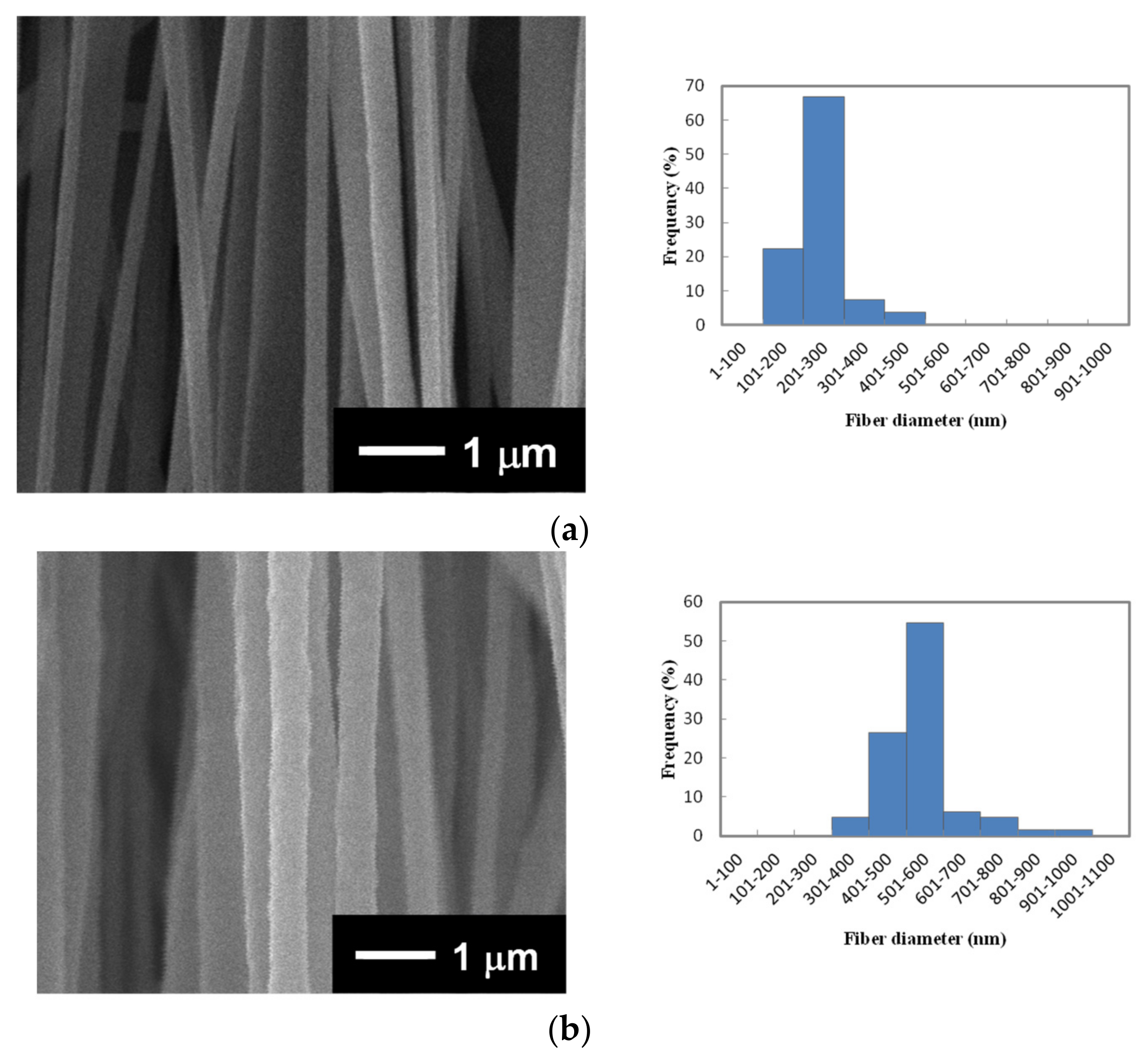
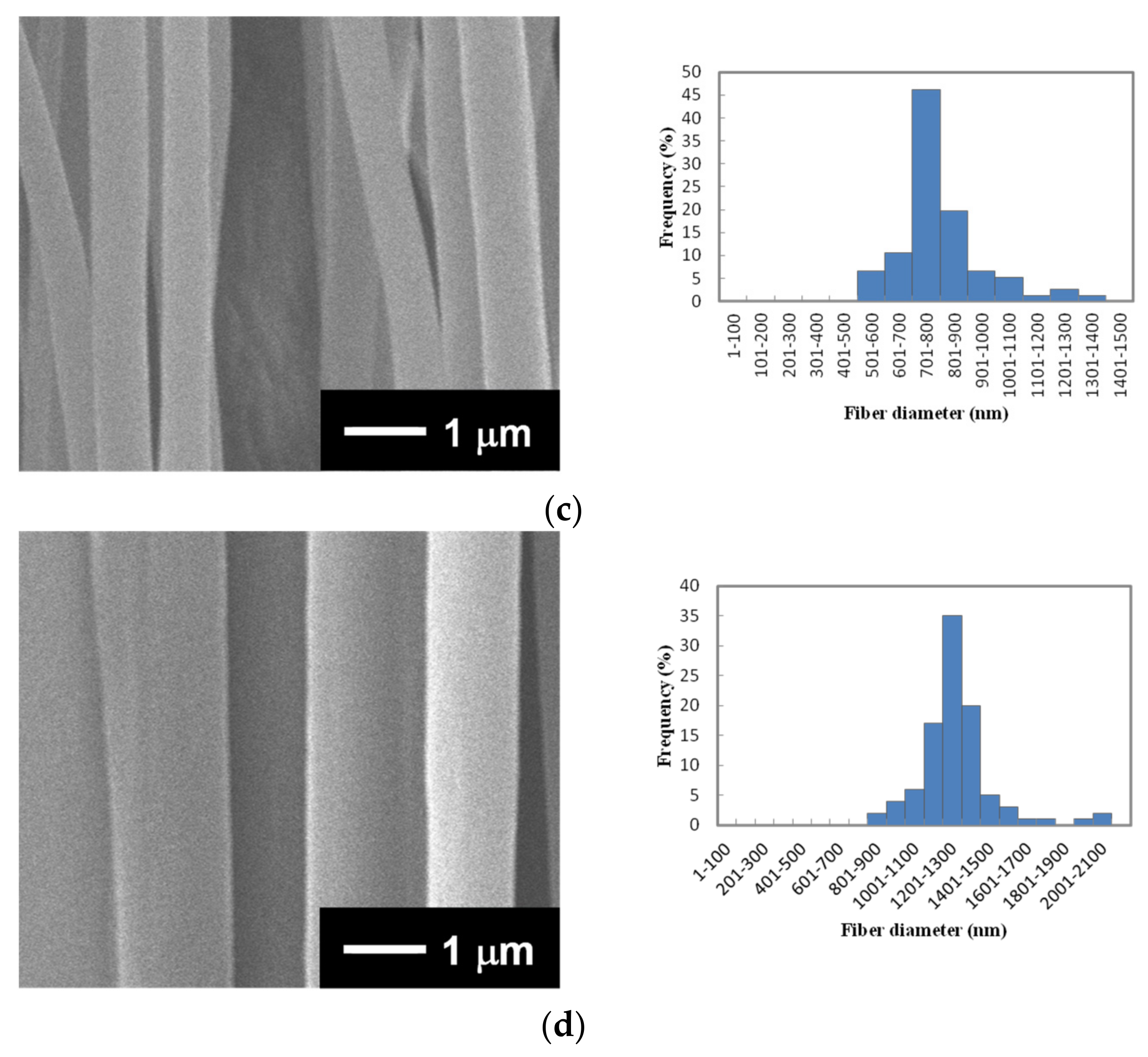
| Sample | Fiber Diameter | Tm [°C] | Xc [%] | ||
|---|---|---|---|---|---|
| [nm] | As-Spun | Hot-Pressed | As-Spun | Hot-Pressed | |
| NF1 | 228 ± 48 | 178 | 180 | 51 | 51 |
| NF2 | 538 ± 114 | 180 | 179 | 51 | 53 |
| NF3 | 823 ± 191 | 179 | 177 | 49 | 50 |
| NF4 | 1315 ± 364 | 178 | 178 | 52 | 52 |
| As-received PVDF a | N.A. | ― | 44 | ― | |
Disclaimer/Publisher’s Note: The statements, opinions and data contained in all publications are solely those of the individual author(s) and contributor(s) and not of MDPI and/or the editor(s). MDPI and/or the editor(s) disclaim responsibility for any injury to people or property resulting from any ideas, methods, instructions or products referred to in the content. |
© 2024 by the authors. Licensee MDPI, Basel, Switzerland. This article is an open access article distributed under the terms and conditions of the Creative Commons Attribution (CC BY) license (https://creativecommons.org/licenses/by/4.0/).
Share and Cite
Priangga Perdana Putra; Akasaka, S.; Konosu, Y.; Zhang, S.; Tanioka, A.; Matsumoto, H. Structure–Piezoelectric Property Relationships of Thin Films Composed of Electrospun Aligned Poly(vinylidene fluoride) Nanofibers. Nanomaterials 2024, 14, 491. https://doi.org/10.3390/nano14060491
Priangga Perdana Putra, Akasaka S, Konosu Y, Zhang S, Tanioka A, Matsumoto H. Structure–Piezoelectric Property Relationships of Thin Films Composed of Electrospun Aligned Poly(vinylidene fluoride) Nanofibers. Nanomaterials. 2024; 14(6):491. https://doi.org/10.3390/nano14060491
Chicago/Turabian StylePriangga Perdana Putra, Shuichi Akasaka, Yuichi Konosu, Shaoling Zhang, Akihiko Tanioka, and Hidetoshi Matsumoto. 2024. "Structure–Piezoelectric Property Relationships of Thin Films Composed of Electrospun Aligned Poly(vinylidene fluoride) Nanofibers" Nanomaterials 14, no. 6: 491. https://doi.org/10.3390/nano14060491