

Advancements in Transparent Conductive Oxides for Photoelectrochemical Applications


 , , and
Abstract
Highlights
- Doping can improve TCO’s electrical conductivity whilst minimizing any significant loss in their optical transmission.
- Further modification techniques increase the surface energy of TCO, reduce particles and defects, and improve electrical conductivity.
- TCO materials show promise for enhancing the efficiency and effectiveness of photoelectrochemical devices.
- Advancements for TCO materials lead to the development of photoelectrochemical conversion technology.
Abstract
1. Introduction
2. TCO Materials
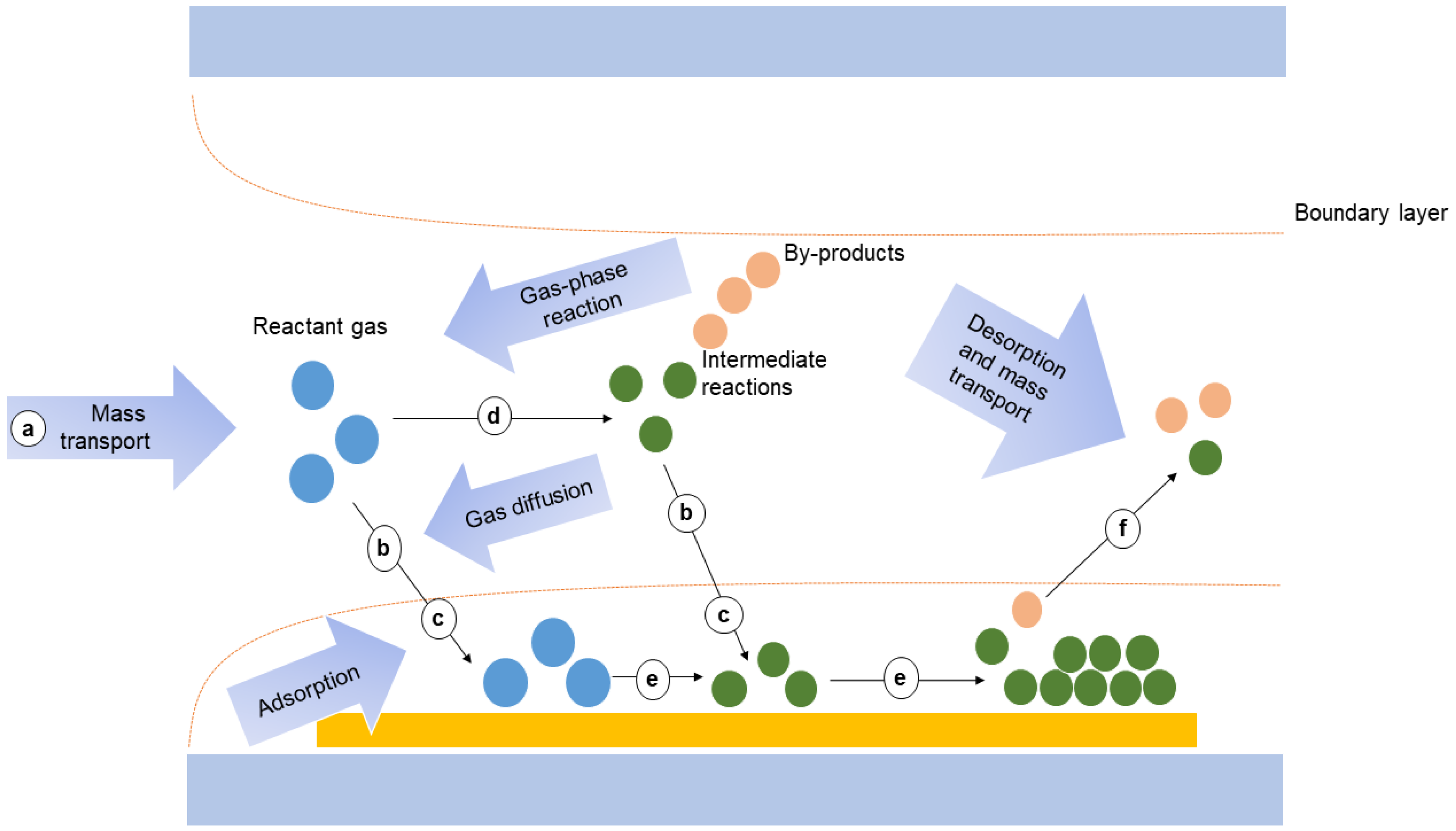
3. Fabrication of TCO Films
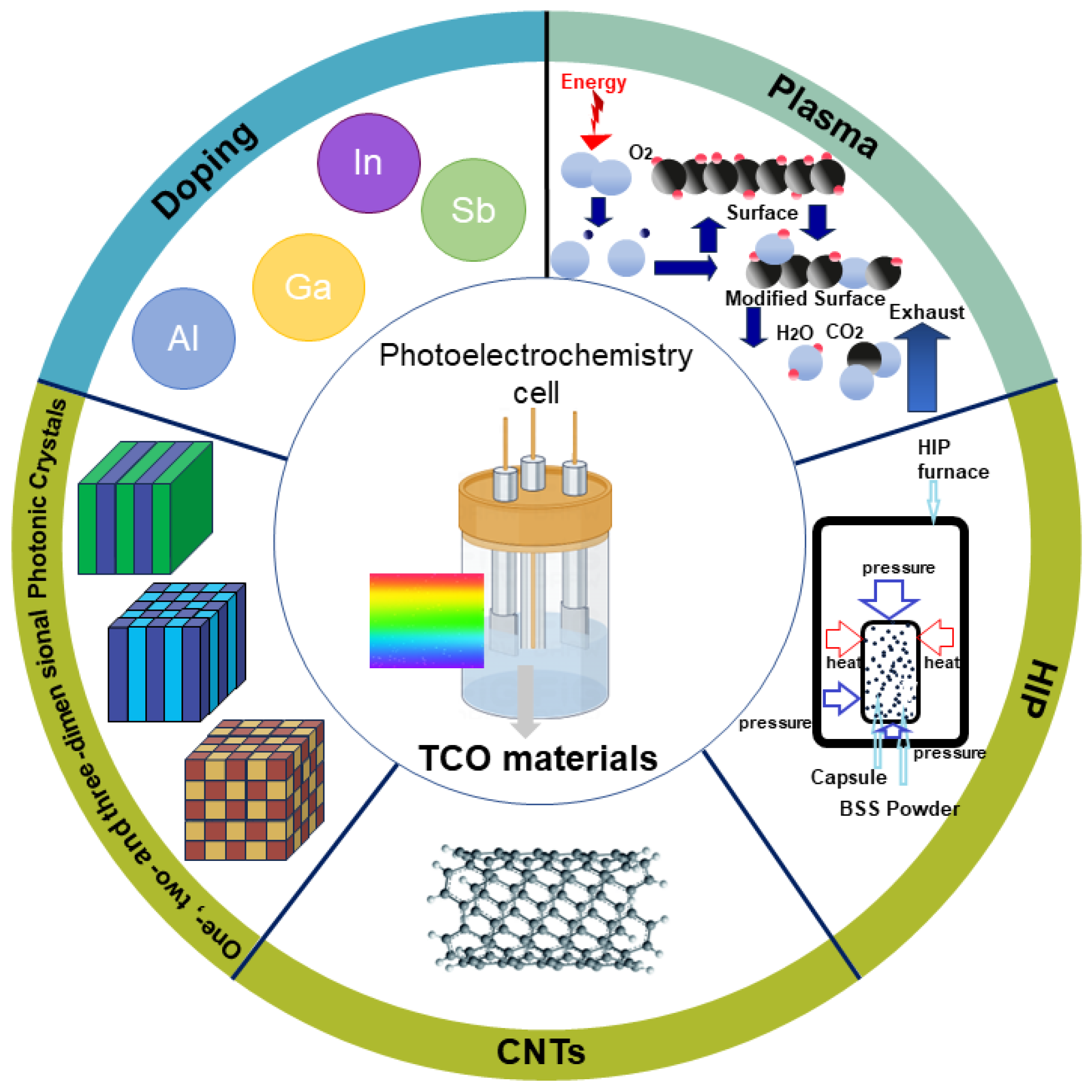
4. Modification Techniques for Improving the Properties of TCO Materials
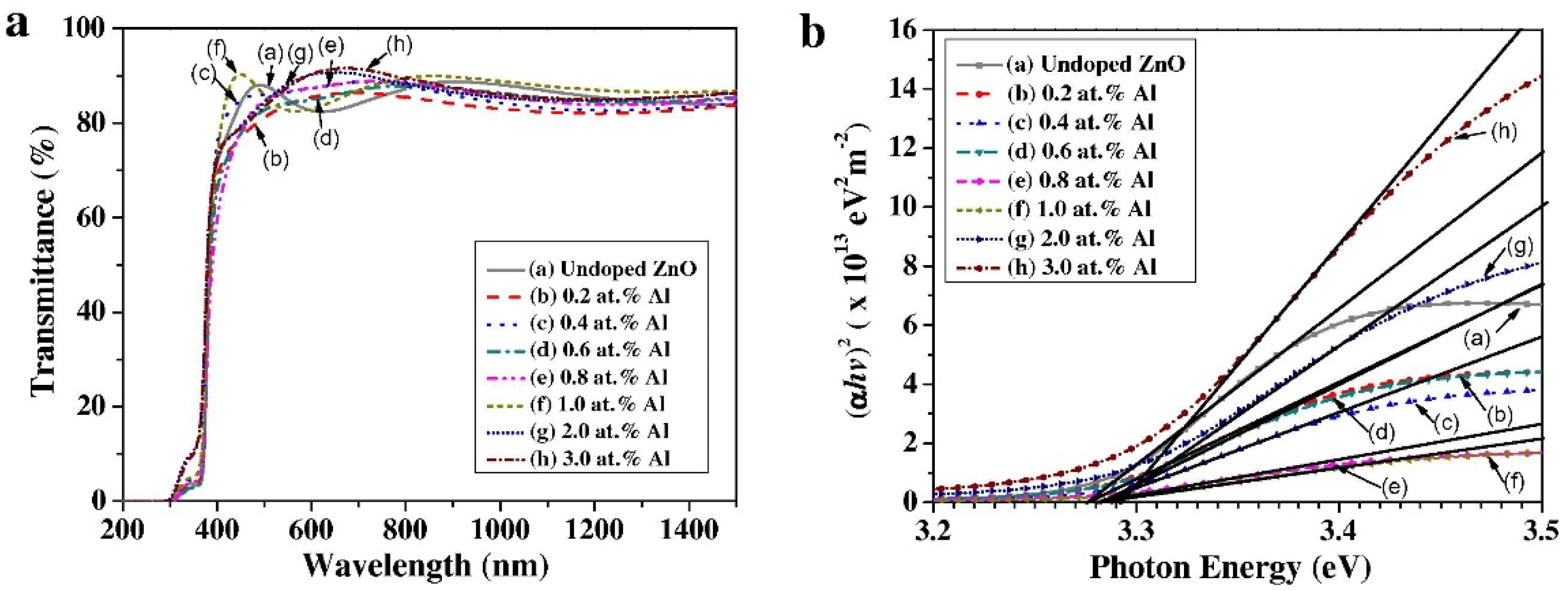
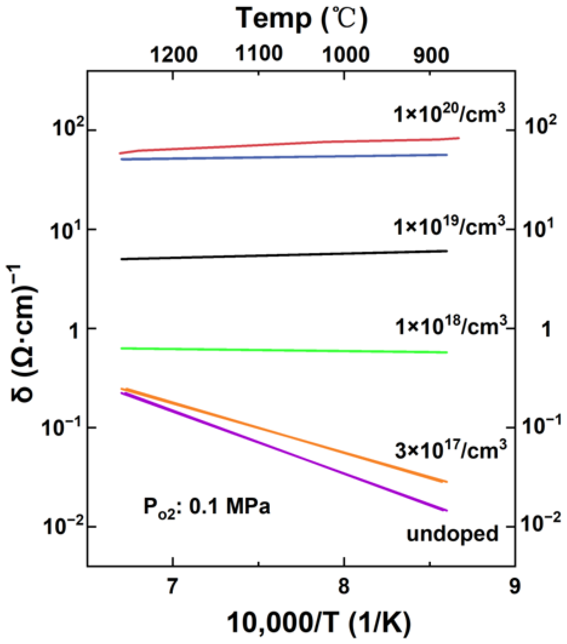
4.1. Element Doping

4.2. Plasma for TCO Materials
4.3. Other Treatments on TCO Materials
5. Conclusions and Future Prospect
- Enhancing transparency and conductivity: Further research is imperative to improve the transparency and conductivity of TCO materials through cost-effective, simple, efficient, and environmentally friendly methods. Current production processes involve expensive materials and intricate procedures, including high-temperature and high-pressure conditions, resulting in elevated production costs. Additionally, ensuring stability under harsh conditions such as acid and alkali corrosion, elevated temperatures, and high moisture levels remains a critical challenge;
- Formulating advanced theories: Advanced theories are essential to investigate reaction mechanisms and establish a comprehensive understanding of the structure–property relationships and carrier transfer mechanisms in TCO materials. Balancing performance indicators such as transparency, electrical conductivity, and mechanical strength during production is crucial but challenging. Developing advanced theories to customize the preparation process is vital for scaling up production;
- Integration of multiple modification strategies: Combining various modification strategi0es, including element doping, plasma treatment, hot isostatic pressing, and carbon nanotube depositing on TCO substrates, holds significant promise. These strategies aim to enhance conductivity and transparency, elevate the rate of PEC reactions, and contribute to environmentally friendly practices, aligning with global sustainability goals.
Author Contributions
Funding
Data Availability Statement
Acknowledgments
Conflicts of Interest
References
- Dincer, I. Renewable energy and sustainable development: A crucial review. Renew. Sust. Energ. Rev. 2000, 4, 157–175. [Google Scholar] [CrossRef]
- Omer, A.M. Energy, environment and sustainable development. Renew. Sust. Energ. Rev. 2008, 12, 2265–2300. [Google Scholar] [CrossRef]
- Zhao, H.; Yuan, Z.Y. Progress and Perspectives for Solar-Driven Water Electrolysis to Produce Green Hydrogen. Adv. Energy Mater. 2023, 13, 2300254. [Google Scholar] [CrossRef]
- Winer, I.; Shter, G.E.; Mann-Lahav, M.; Grader, G.S. Effect of solvents and stabilizers on sol–gel deposition of Ga-doped zinc oxide TCO films. J. Mate. Res. 2011, 26, 1309–1315. [Google Scholar] [CrossRef]
- Song, D.; Widenborg, P.; Chin, W.; Aberle, A.G. Investigation of lateral parameter variations of Al-doped zinc oxide films prepared on glass substrates by rf magnetron sputtering. Sol. Energy Mater. Sol. Cells 2002, 73, 1–20. [Google Scholar] [CrossRef]
- Macco, B.; Wu, Y.; Vanhemel, D.; Kessels, W.M.M. High mobility In2O3:H transparent conductive oxides prepared by atomic layer deposition and solid phase crystallization. Phys. Status Solidi Rapid Res. Lett. 2014, 8, 987–990. [Google Scholar] [CrossRef]
- Minami, T. Present status of transparent conducting oxide thin-film development for Indium-Tin-Oxide (ITO) substitutes. Thin Solid Films 2008, 516, 5822–5828. [Google Scholar] [CrossRef]
- Sohn, S.; Han, Y.S. Transparent conductive oxide (TCO) films for organic light emissive devices (OLEDs). Org. Light. Emit. Diode-Mater. Process Devices 2011, 233–274. [Google Scholar] [CrossRef]
- Qiu, T.; Akinoglu, E.M.; Luo, B.; Konarova, M.; Yun, J.; Gentle, I.R. Nanosphere lithography: A versatile approach to develop transparent conductive films for optoelectronic applications. Adv. Mater. 2022, 34, 2103842. [Google Scholar] [CrossRef]
- Sharma, M.; Chaudhary, D.; Dwivedi, N.; Sudhakar, S.; Kumar, S. Simulating the role of TCO materials, their surface texturing and band gap of amorphous silicon layers on the efficiency of amorphous silicon thin film solar cells. Silicon 2017, 9, 59–68. [Google Scholar] [CrossRef]
- Gong, J.; Sumathy, K.; Liang, J. A simplified electrical model of the dye-sensitised photoelectrochemical cell. Int. J. Sustain. Energy 2016, 35, 75–87. [Google Scholar] [CrossRef]
- Minami, T. Transparent conducting oxide semiconductors for transparent electrodes. Semicond. Sci. Technol. 2005, 20, S35. [Google Scholar] [CrossRef]
- Aïssa, B.; Abdallah, A.A.; Garcia, J.L. Field assessment of Transparent Conductive Oxides Stability Under Outdoor Conditions. In Proceedings of the 2022 IEEE 49th Photovoltaics Specialists Conference (PVSC), Philadelphia, PA, USA, 5–10 June 2000. [Google Scholar] [CrossRef]
- Aouaj, M.A.; Diaz, R.; Belayachi, A.; Rueda, F.; Abd-Lefdil, M. Comparative study of ITO and FTO thin films grown by spray pyrolysis. Mater. Res. Bull. 2009, 44, 1458–1461. [Google Scholar] [CrossRef]
- Khan, Z.R.; Shkir, M.; Ganesh, V.; AlFaify, S.; Yahia, I.S.; Zahran, H.Y. Linear and nonlinear optics of CBD grown nanocrystalline F doped CdS thin films for optoelectronic applications: An effect of thickness. J. Electron. Mater. 2018, 47, 5386–5395. [Google Scholar] [CrossRef]
- Fallah, H.R.; Ghasemi, M.; Hassanzadeh, A.; Steki, H. The effect of annealing on structural, electrical and optical properties of nanostructured ITO films prepared by e-beam evaporation. Mater. Res. Bull. 2007, 42, 487–496. [Google Scholar] [CrossRef]
- Morales-Masis, M.; Rucavado, E.; Monnard, R.; Barraud, L.; Holovský, J.; Despeisse, M.; Boccard, M.; Ballif, C. Highly conductive and broadband transparent Zr-doped In2O3 as front electrode for solar cells. IEEE J. Photovolt. 2018, 8, 1202–1207. [Google Scholar] [CrossRef]
- Shinde, S.S.; Shinde, P.S.; Bhosale, C.H.; Rajpure, K.Y. Optoelectronic properties of sprayed transparent and conducting indium doped zinc oxide thin films. J. Phys. D 2008, 41, 105109. [Google Scholar] [CrossRef]
- Markova, N.; Pikulev, V.; Berezina, O.; Pergament, A.; Kolobova, E. Spectral dependence of photocurrent of UV sensor based on In-Zn oxide nanofibers. In AIP Conference Proceedings; AIP Publishing: College Park, MA, USA, 2020. [Google Scholar] [CrossRef]
- Ma, J.; Ji, F.; Ma, H.; Li, S. Preparation and characterization of ZnO films by an evaporating method. J. Vac. Sci. Technol. A 1995, 13, 92–94. [Google Scholar] [CrossRef]
- Salavati-Niasari, M.; Davar, F.; Khansari, A. Nanosphericals and nanobundles of ZnO: Synthesis and characterization. J. Alloys Compd. 2011, 509, 61–65. [Google Scholar] [CrossRef]
- Liu, X.P.; Zhen, T.L.; Xiong, J.P. Effect of UV Radiation on Electrochemical Behavior of Polyurea Polyaspartic Ester Coating in 3.5% NaCl by EIS. Int. J. Electrochem. Sci. 2013, 8, 11723–11733. [Google Scholar] [CrossRef]
- Das, C.; Richter, M.; Tallarida, M.; Schmeißer, D. Electronic properties of atomic layer deposition films, anatase and rutile TiO2 studied by resonant photoemission spectroscopy. J. Phys. D Appl. Phys. 2016, 49, 275304. [Google Scholar] [CrossRef]
- Kaleemulla, S.; Reddy, A.S.; Uthanna, S.; Reddy, P.S. Physical properties of In2O3 thin films prepared at various oxygen partial pressures. J. Alloys Compd. 2009, 479, 589–593. [Google Scholar] [CrossRef]
- Liu, J.; Zhao, Y.; Zhang, J.N.; Ye, J.H.; Ma, X.N.; Ke, J. Construction of Cu2O/In2O3 hybrids with p–n heterojunctions for enhanced photocatalytic performance. J. Nanosci. Nanotechnol. 2019, 19, 7689–7695. [Google Scholar] [CrossRef] [PubMed]
- Pugalenthi, A.S.; Balasundaraprabhu, R.; Gunasekaran, V.; Muthukumarasamy, N.; Prasanna, S.; Jayakumar, S. Effect of thickness on the structural, optical and electrical properties of RF magnetron sputtered GZO thin films. Mater. Sci. Semicond. Process. 2015, 29, 176–182. [Google Scholar] [CrossRef]
- Wang, H.; Sun, Y.; Fang, L.; Wang, L.; Chang, B.; Sun, X.; Ye, L. Growth and characterization of high transmittance GZO films prepared by sol-gel method. Thin Solid Films 2016, 615, 19–24. [Google Scholar] [CrossRef]
- Anand, V.; Sakthivelu, A.; Kumar, K.D.A.; Valanarasu, S.; Ganesh, V.; Shkir, M.; Kathalingam, A.; AlFaify, S. Novel rare earth Gd and Al co-doped ZnO thin films prepared by nebulizer spray method for optoelectronic applications. Superlattices Microstruct. 2018, 123, 311–322. [Google Scholar] [CrossRef]
- Challali, F.; Mendil, D.; Touam, T.; Chauveau, T.; Bockelée, V.; Sanchez, A.G.; Chelouche, A.; Besland, M.P. Effect of RF sputtering power and vacuum annealing on the properties of AZO thin films prepared from ceramic target in confocal configuration. Mat. Sci. Semicond. Proc. 2020, 118, 105217. [Google Scholar] [CrossRef]
- Kawska, A.; Duchstein, P.; Hochrein, O.; Zahn, D. Atomistic mechanisms of ZnO aggregation from ethanolic solution: Ion association, proton transfer, and self-organization. Nano Lett. 2008, 8, 2336–2340. [Google Scholar] [CrossRef] [PubMed]
- Kim, K.W.; Choi, N.J.; Kim, K.B.; Kim, M.; Lee, S.N. Growth and characterization of nonpolar (10-10) ZnO transparent conductive oxide on semipolar (11–22) GaN-based light-emitting diodes. J. Alloys Compd. 2017, 666, 88. [Google Scholar] [CrossRef]
- Liu, W.H.; Shieu, F.S.; Hsiao, W.T. AZO photocatalytic coating deposited by plasma thermal spraying with shell-type feedstock powder. J. Eur. Ceram. Soc. 2017, 37, 2857–2869. [Google Scholar] [CrossRef]
- Yao, T.; An, X.; Han, H.; Chen, J.Q.; Li, C. Photoelectrocatalytic materials for solar water splitting. Adv. Energy Mater. 2018, 8, 1800210. [Google Scholar] [CrossRef]
- Mamat, M.H.; Sahdan, M.Z.; Khusaimi, Z.; Ahmed, A.Z.; Abdullah, S.; Rusop, M. Influence of doping concentrations on the aluminum doped zinc oxide thin films properties for ultraviolet photoconductive sensor applications. Opt. Mater. 2010, 32, 696–699. [Google Scholar] [CrossRef]
- Govatsi, K.; Syrrokostas, G.; Yannopoulos, S.N.; Neophytides, S.G. Optimization of aluminum doped ZnO nanowires for photoelectrochemical water splitting. Electrochim. Acta 2021, 392, 138995. [Google Scholar] [CrossRef]
- Elhamali, O.S.; Akhil, M.N.; Abusabee, K.M.; Kalfagiannis, N.; Koutsogeorgis, D. Environmental stability evaluation of aluminium doped zinc oxide (azo) transparent electrodes deposited at low temperature for solar cells. J. Sol. Energy Sustain. Dev. 2022, 11, 1–12. [Google Scholar] [CrossRef]
- Bouznit, Y.; Henni, A. Enhanced photoelectrochemical performance of Al-doped ZnO thin films prepared by co-spray technique. Mat. Sci. Semicon. Proc. 2020, 118, 105208. [Google Scholar] [CrossRef]
- Cheong, K.Y.; Muti, N.; Ramanan, S.R. Electrical and optical studies of ZnO: Ga thin films fabricated via the sol–gel technique. Thin Solid Films 2002, 410, 142–146. [Google Scholar] [CrossRef]
- Kono, A.; Nagai, T.; Shoji, F. Contribution to carrier densities of the oxygen vacancy in a low-resistivity tin-doped indium oxide film by the hot-cathode plasma sputtering method. Mater. Lett. 2010, 64, 622–624. [Google Scholar] [CrossRef]
- Tseng, S.F.; Hsiao, W.T.; Huang, K.C.; Chiang, D.; Chen, M.F.; Chou, C.P. Laser scribing of indium tin oxide (ITO) thin films deposited on various substrates for touch panels. Appl. Surf. Sci. 2010, 257, 1487–1494. [Google Scholar] [CrossRef]
- Senthilkumar, V.; Senthil, K.; Vickraman, P. Microstructural, electrical and optical properties of indium tin oxide (ITO) nanoparticles synthesized by co-precipitation method. Mater. Res. Bull. 2012, 47, 1051–1056. [Google Scholar] [CrossRef]
- Cao, W.; Li, J.; Chen, H.; Xue, J. Transparent electrodes for organic optoelectronic devices: A review. J. Photonics Energy 2014, 4, 40990–41018. [Google Scholar] [CrossRef]
- Akanda, M.R.; Osman, A.M.; Nazal, M.K.; Aziz, M.A. Recent advancements in the utilization of indium tin oxide (ITO) in electroanalysis without surface modification. J. Electrochem. Soc. 2020, 167, 037534. [Google Scholar] [CrossRef]
- Wang, T.; Lu, K.; Xu, Z.; Lin, Z.; Ning, H.; Qiu, T.; Yang, Z.; Zheng, H.; Yao, R.; Peng, J. Recent developments in flexible transparent electrode. Crystals 2021, 11, 511. [Google Scholar] [CrossRef]
- Cirocka, A.; Zarzeczańska, D.; Wcisło, A. Good Choice of Electrode Material as the Key to Creating Electrochemical Sensors—Characteristics of Carbon Materials and Transparent Conductive Oxides (TCO). Materials 2021, 14, 4743. [Google Scholar] [CrossRef] [PubMed]
- Benck, J.D.; Pinaud, B.A.; Gorlin, Y.; Jaramillo, T.F. Substrate selection for fundamental studies of electrocatalysts and photoelectrodes: Inert potential windows in acidic, neutral, and basic electrolyte. PLoS ONE 2014, 9, e107942. [Google Scholar] [CrossRef]
- Zhu, B.L.; Peng, H.; Tao, Y.; Wu, J.; Shi, X.W. Highly transparent conductive F-doped SnO2 films prepared on polymer substrate by radio frequency reactive magnetron sputtering. Thin Solid Films 2022, 756, 139360. [Google Scholar] [CrossRef]
- Zhou, Y.; Liu, Z.; He, C.; Yin, C. Evolution of defects and charge carrier transport mechanism in fluorine-doped tin oxide thin films upon thermal treatment. J. Appl. Phys. 2021, 130, 135702. [Google Scholar] [CrossRef]
- van Mol, A.M.B.; Chae, Y.; McDaniel, A.H.; Allendorf, M.D. Chemical vapor deposition of tin oxide: Fundamentals and applications. Thin Solid Films 2005, 502, 72–78. [Google Scholar] [CrossRef]
- Yang, J.L.; An, S.J.; Park, W.I.; Yi, G.C.; Choi, W. Photocatalysis using ZnO thin films and nanoneedles grown by metal–organic chemical vapor deposition. Adv. Mater. 2004, 16, 1661–1664. [Google Scholar] [CrossRef]
- Terasako, T.; Yura, S.; Azuma, S.; Shimomura, S.; Shirakata, S.; Yagi, M. Comparative study on structural and optical properties of ZnO films grown by metalorganic molecular beam deposition and metalorganic chemical vapor deposition. J. Vac. Sci. Technol. B 2009, 27, 1609–1614. [Google Scholar] [CrossRef]
- Elen, K.; Capon, B.; De Dobbelaere, C.; Dewulf, D.; Peys, N.; Detavernier, C.; Hardy, A.; Van Bael, M.K. Transparent conducting oxide films of group V doped titania prepared by aqueous chemical solution deposition. Thin Solid Films 2014, 555, 33–38. [Google Scholar] [CrossRef]
- Kadari, A.S.; Ech-Chergui, A.N.; Aïssa, B.; Mukherjee, S.K.; Benaioun, N.; Zakaria, Y.; Zekri, A.; Reda, C.M.; Mehdi, A.; Rabea, R.; et al. Growth and characterization of transparent vanadium doped zinc oxide thin films by means of a spray pyrolysis process for TCO application. J. Sol Gel Sci. Technol. 2022, 103, 691–703. [Google Scholar] [CrossRef]
- Jahn, R.; Löbmann, P. Microstructure and performance of AZO thin films prepared by sol–gel processing. J. Sol Gel Sci. Technol. 2013, 66, 120–125. [Google Scholar] [CrossRef]
- Socol, M.; Preda, N.; Rasoga, O.; Costas, A.; Stanculescu, A.; Breazu, C.; Gherendi, F.; Socol, G. Pulsed Laser Deposition of Indium Tin Oxide Thin Films on Nanopatterned Glass Substrates. Coatings 2019, 9, 19. [Google Scholar] [CrossRef]
- Kim, D.H.; Heo, J.H.; Kwak, D.J.; Sung, Y.M. Synthesis of TCO-free Dye-sensitized Solar Cells with Nanoporous Ti Electrodes Using RF Magnetron Sputtering Technology. J. Electr. Eng. Technol. 2010, 5, 146–150. [Google Scholar] [CrossRef][Green Version]
- Liu, X.; Cao, L.; Guo, Z.; Li, Y.; Gao, W.; Zhou, L. A review of perovskite photovoltaic materials’ synthesis and applications via chemical vapor deposition method. Materials 2019, 12, 3304. [Google Scholar] [CrossRef] [PubMed]
- Hazbun, R.; Hart, J.; Hickey, R.; Ghosh, A.; Fernando, N.; Zollner, S.; Adam, T.N.; Kolodzey, J. Silicon epitaxy using tetrasilane at low temperatures in ultra-high vacuum chemical vapor deposition. J. Cryst. Growth 2016, 444, 21–27. [Google Scholar] [CrossRef]
- Lin, L.; Deng, B.; Sun, J.; Peng, H.; Liu, Z. Bridging the gap between reality and ideal in chemical vapor deposition growth of graphene. Chem. Rev. 2018, 118, 9281–9343. [Google Scholar] [CrossRef] [PubMed]
- Bozzo, S.; Lazzari, J.L.; Coudreau, C.; Ronda, A.; d’Avitaya, F.A.; Derrien, J.; Mesters, S.; Hollaender, B.; Gergaud, P.; Thomas, O. Chemical vapor deposition of silicon–germanium heterostructures. J. Cryst. Growth 2000, 216, 171–184. [Google Scholar] [CrossRef]
- Faÿ, S.; Steinhauser, J.; Oliveira, N.; Vallat-Sauvain, E.; Ballif, C. Opto-electronic properties of rough LP-CVD ZnO: B for use as TCO in thin-film silicon solar cells. Thin Solid Films 2007, 515, 8558–8561. [Google Scholar] [CrossRef]
- Meier, J.; Kroll, U.; Dubail, S.; Golay, S.; Fay, S.; Dubail, J.; Shah, A. Efficiency enhancement of amorphous silicon pin solar cells by LP-CVD ZnO. In Proceedings of the Conference Record of the Twenty-Eighth IEEE Photovoltaic Specialists Conference-2000 (Cat. No. 00CH37036), Anchorage, AK, USA, 15–22 September 2000. [Google Scholar] [CrossRef][Green Version]
- Kashyap, A.; Singh, N.K.; Soni, M.; Soni, A. Deposition of thin films by chemical solution-assisted techniques. In Chemical Solution Synthesis for Materials Design and Thin Film Device Applications; Elsevier: Amsterdam, The Netherlands, 2021; Chapter 3; pp. 79–117. [Google Scholar] [CrossRef]
- Dagkaldiran, Ü.; Gordijn, A.; Finger, F.; Yates, H.M.; Evans, P.; Shell, D.W.; Remes, Z.; Vanecek, M. Amorphous silicon solar cells made with SnO2: F TCO films deposited by atmospheric pressure CVD. Mater. Sci. Eng. B 2009, 159, 6–9. [Google Scholar] [CrossRef]
- Leng, J.; Wang, Z.; Wang, J.; Wu, H.H.; Yan, G.; Li, X.; Guo, H.; Liu, Y.; Zhang, Q.; Guo, Z. Advances in nanostructures fabricated via spray pyrolysis and their applications in energy storage and conversion. Chem. Soc. Rev. 2019, 48, 3015–3072. [Google Scholar] [CrossRef]
- Rubloff, G.W.; Bordonaro, D.T. Integrated processing for microelectronics science and technology. IBM J. Res. Dev. 1992, 36, 233–276. [Google Scholar] [CrossRef]
- Miccoli, I.; Spampinato, R.; Marzo, F.; Prete, P.; Lovergine, N. DC-magnetron sputtering of ZnO:Al films on (00.1)Al2O3 substrates from slip-casting sintered ceramic targets. Appl. Surf. Sci. 2014, 313, 418–423. [Google Scholar] [CrossRef]
- Ide, T.; Hossain, M.A.; Nakamura, Y.; Ohtsu, Y. Rotational cross-shaped magnetized radio-frequency sputtering plasma source for uniform circular target utilization. J. Vac. Sci. Technol. A 2017, 35, 061312. [Google Scholar] [CrossRef]
- Giménez, S.; Bisquert, J. Photoelectrochemical Solar Fuel Production, From Basic Principle to Advanced Devices; Springer: Cham, Switzerland, 2016; p. 559. [Google Scholar] [CrossRef]
- Schmidt, J.; Cuevas, A. Electronic properties of light-induced recombination centers in boron-doped Czochralski silicon. J. Appl. Phys. 1999, 86, 3175–3180. [Google Scholar] [CrossRef]
- Hurma, T.; Caglar, M. Effect of anionic fluorine incorporation on structural, optical and electrical properties of ZnO nanocrystalline films. Mater. Sci. Semicond. Process. 2020, 110, 104949. [Google Scholar] [CrossRef]
- Hafdallah, A.; Ynineb, F.; Aida, M.S.; Attaf, N. In doped ZnO thin films. J. Alloys Compd. 2011, 509, 7267–7270. [Google Scholar] [CrossRef]
- Das, K.A.; Misra, P.; Ajimsha, R.S.; Bose, A.; Joshi, S.C.; Phase, D.M.; Kukreja, L.M. Studies on temperature dependent semiconductor to metal transitions in ZnO thin films sparsely doped with Al. J. Appl. Phys. 2012, 112, 103706. [Google Scholar] [CrossRef]
- Miyazaki, M.; Sato, K.; Mitsui, A.; Nishimura, H. Properties of Ga-doped ZnO films. J. Non Cryst. Solids 1997, 218, 323–328. [Google Scholar] [CrossRef]
- Keskenler, E.F.; Turgut, G.; Doğan, S. Investigation of structural and optical properties of ZnO films co-doped with fluorine and ind0.ium. Superlattices Microstruct. 2012, 52, 107–115. [Google Scholar] [CrossRef]
- Baik, D.G.; Cho, S.M. Application of sol-gel derived films for ZnO/n-Si junction solar cells. Thin Solid. Films 1999, 354, 227–231. [Google Scholar] [CrossRef]
- Zhou, Z.; Zou, M.; Xu, Y.; Lan, J.; Liu, C.; Ahmad, A.; Lin, Y.H.; Nan, C.W. High thermoelectric performance of high-mobility Ga-doped ZnO films via homogenous interface design. J. Am. Ceram. Soc. 2021, 104, 3992–3999. [Google Scholar] [CrossRef]
- Wang, R.; Sleight, A.W.; Cleary, D. High Conductivity in Gallium-Doped Zinc Oxide Powders. Chem. Mater. 1996, 8, 433–439. [Google Scholar] [CrossRef]
- Muchuweni, E.; Sathiaraj, T.S.; Nyakotyo, H. Effect of gallium doping on the structural, optical and electrical properties of zinc oxide thin films prepared by spray pyrolysis. Ceram. Int. 2016, 42, 10066–10070. [Google Scholar] [CrossRef]
- Dey, K. High Mobility and Highly Transparent Cerium Doped Indium Oxide Films Deposited by Magnetron Sputtering for Photovoltaic Applications. Master’s Thesis, National University of Singapore, Singapore, 23 July 2018. [Google Scholar]
- Rajni, K.S.; Raguram, T. Doped Semiconductor as photoanode. In Interfacial Engineering in Functional Materials for Dye-Sensitized Solar Cells; Wiley: New Yok, NY, USA, 2019. [Google Scholar] [CrossRef]
- Dien, E.; Laurent, J.M.; Smith, A. Comparison of optical and electrical characteristics of SnO2-based thin films deposited by pyrosol from different tin precursors. J. Eur. Ceram. Soc. 1999, 19, 787–789. [Google Scholar] [CrossRef]
- Su, K.; Mao, Z.; Yang, Z.; Zhang, J. Preparation and characterization of PVC/CsxWO3 composite film with excellent near-infrared light shielding and high visible light transmission. J. Vinyl Addit. Technol. 2021, 27, 356–366. [Google Scholar] [CrossRef]
- Floriano, E.A.; Scalvi, L.V.A.; Sambrano, J.R.; de Andrade, A. Decay of photo-induced conductivity in Sb-doped SnO2 thin films, using monochromatic light of about bandgap energy. Appl. Surf. Sci. 2013, 267, 164–168. [Google Scholar] [CrossRef]
- Mazloom, J.; Ghodsi, F.E.; Gholami, M. Fiber-like stripe ATO (SnO2: Sb) nanostructured thin films grown by sol–gel method: Optical, topographical and electrical properties. J. Alloys Compd. 2013, 579, 384–393. [Google Scholar] [CrossRef]
- Samanta, S.; Paramanik, B.; Das, D. Structural characteristics, impedance spectroscopy, ac-conductivity and dielectric loss studies on RF-magnetron sputtered F doped ZnO (FZO) thin films. Ceram. Int. 2022, 48, 31370–31380. [Google Scholar] [CrossRef]
- Das, A.K.; Ajimsha, R.S.; Kukreja, L.M. Quantum corrections to temperature dependent electrical conductivity of ZnO thin films degenerately doped with Si. Appl. Phys. Lett. 2014, 104, 042112. [Google Scholar] [CrossRef]
- Frotes, G.M. Anionic Segregation of Chloride and Fluoride Doped-Nano ZnO: Microstructure Evolution, Electrical Conductivity and Photocatalysis. Ph.D. Thesis, University of São Paulo, Cidade Universitária, São Paulo, Brazil, 30 September 2022. [Google Scholar]
- Qasim, A.K.; Jamil, L.A.; Qiao, C. Enhanced Photoelectrochemical Water Splitting of Hydrothermally-Grown ZnO and Yttrium-doped ZnO NR Arrays. IOP Conf. Ser. Mater. Sci. Eng. 2018, 454, 012033. [Google Scholar] [CrossRef]
- Maertens, A.; Margueron, S.; Genty, F.; Kuprenaite, S.; Abrutis, A.; Legrani, O. Elaboration of In2O3–ZnO Thin Films for Mid-Infrared Transparent Electrode Applications. J. Nanoelectron. Optoelectron. 2015, 10, 295–300. [Google Scholar] [CrossRef]
- Gupta, R.K.; Ghosh, K.; Mishra, S.R.; Kahol, P.K. Structural, optical and electrical characterization of highly conducting Mo-doped In2O3 thin films. Appl. Surf. Sci. 2008, 254, 4018–4023. [Google Scholar] [CrossRef]
- Feng, X.; Ren, S.; Li, K.; Zhang, R.; Chen, J.; Li, Y.; Jiang, Y.; He, Z.; Zhu, J.; Meng, W.; et al. Ultra-Tiny Sb-Doped SnO2 Nanoparticles as a Superior Catalyst for Vanadium Redox Reactions. J. Electrochem. Soc. 2020, 167, 100522. [Google Scholar] [CrossRef]
- Liu, X.M.; Wu, S.L.; Chu, P.K.; Zheng, J.; Li, S.L. Characteristics of nano Ti-doped SnO2 powders prepared by sol–gel method. Mater. Sci. Eng. A 2006, 426, 274–277. [Google Scholar] [CrossRef]
- Senoo, Y.; Kakinuma, K.; Uchida, M.; Uchida, M.; Dekia, S.; Watanabe, M. Improvements in electrical and electrochemical properties of Nb-doped SnO2−δ supports for fuel cell cathodes due to aggregation and Pt loading. RSC Adv. 2014, 4, 32180–32188. [Google Scholar] [CrossRef]
- Mulmi, D.D.; Sekiya, T.; Kamiya, N.; Kurita, S.; Murakami, Y.; Kodaira, T. Optical and electric properties of Nb-doped anatase TiO2 single crystal. J. Phys. Chem. Solids 2004, 65, 1181–1185. [Google Scholar] [CrossRef]
- Aydoğu, H.S.; Çabuk, G.; Çoban, M.B. The Effects of Different Ga Doping on Structural, Optical and Electrical Properties of CdO Films. Süleyman Demirel Üniversitesi Fen Bilim. Enstitüsü Derg. 2019, 23, 140–147. [Google Scholar] [CrossRef]
- Velusamy, P.; Babu, R.R.; Ramamurthi, K.; Elangovan, E.; Viegas, J.; Sridharan, M. Gas sensing and opto-electronic properties of spray deposited cobalt doped CdO thin films. Sens. Actuator B Chem. 2018, 255, 871–883. [Google Scholar] [CrossRef]
- Ahmadi, M.; Anaghizi, S.J.; Asemi, M.; Ghanaatshoar, M. Plasma-treated room temperature synthesized CuCrO2/Au/CuCrO2 on Polyethylene terephthalate: Towards a high-performance flexible p-type transparent conductor. Thin Solid. Films 2021, 723, 138582. [Google Scholar] [CrossRef]
- Major, S.; Kumar, S.; Bhatnagar, M.; Chopra, K.L. Effect of hydrogen plasma treatment on transparent conducting oxides. Appl. Phys. Lett. 1986, 49, 394–396. [Google Scholar] [CrossRef]
- Sun, D. Surface modification of natural fibers using plasma treatment. In Biodegradable Green Compos; Wiley: New York, NY, USA, 2016; pp. 18–39. [Google Scholar] [CrossRef]
- Uematsu, K.; Kato, Z.; Uchida, N.; Saito, K. Eletrical Conductivity of Antimony-Doped Tin Dioxide Prepared by Hot Isostatic Pressing. J. Am. Ceram. Soc. 1987, 70, 142–143. [Google Scholar] [CrossRef]
- Basiuk, E.V.; Ramírez-Calera, I.J.; Meza-Laguna, V.; Abarca-Morales, E.; Pérez-Rey, L.A.; Re, M.; Prete, P.; Lovergine, N.; Álvarez-Zauco, E.; Basiuk, V. Solvent-free functionalization of carbon nanotube buckypaper with amines. Appl. Surf. Sci. 2015, 357, 1355–1368. [Google Scholar] [CrossRef]
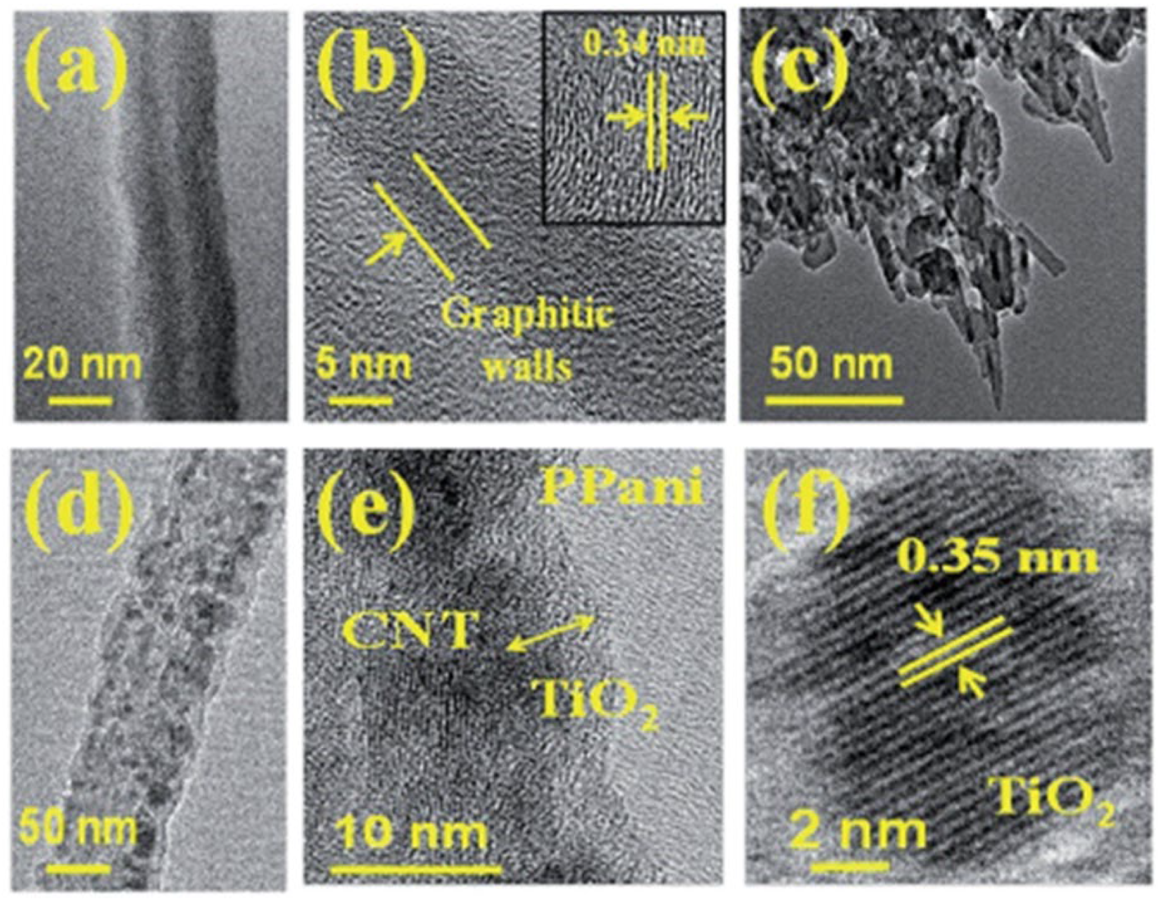
- Baro, M.; Hussain, A.A.; Pal, A.R. Enhanced light sensing performance of a hybrid device developed using as-grown vertically aligned multiwalled carbon nanotubes on TCO substrates. RSC Adv. 2014, 87, 46970–46975. [Google Scholar] [CrossRef]
- Maiti, U.N.; Lee, W.J.; Lee, J.M.; Oh, Y.; Kim, J.Y.; Kim, J.E.; Shim, J.; Han, T.H.; Kim, S.O. 25th anniversary article: Chemically modified/doped carbon nanotubes & graphene for optimized nanostructures & nanodevices. Adv. Mater. 2013, 26, 40–67. [Google Scholar] [CrossRef]
- Zhang, M. Ordered Transparent Conductive Oxides (TCOs) for Applications to Photoelectrochemistry. Ph.D. Thesis, University of York, York, UK, 21 October 2016. [Google Scholar]
- Wang, K.; Ke, X.; Wang, W.; Tu, C.; Luo, D.; Zhang, M. The impacts of fluorine-doped tin oxide photonic crystals on a cadmium sulfide-based photoelectrode for improved solar energy conversion under lower incidence. Catalysts 2022, 10, 1252. [Google Scholar] [CrossRef]


| TCO Material | Transparency | Conductivity | Thermal Stability | Chemical Stability | Eg |
|---|---|---|---|---|---|
| Fluorine-doped tin oxide (FTO) | High (80–90%) | Good (cm−1) [14] | Excellent | Relatively stable to strong acids and alkalis | Approx. 3.5–4 eV [15] |
| Indium tin oxide (ITO) | High (80–90%) | Good (cm−1) [16] | Ordinary | Easily corroded under strong acids and alkalis | Approx. 3.5–4 eV [17] |
| Indium zinc oxide (IZO) | High (80–90%) | cm−1) [18] | Excellent | Easily corroded under strong acids and alkalis | Approx. 3.5–4 eV [19] |
| Zinc oxide (ZnO) | High (80–90%) | cm−1) [20] | Excellent | Corrosion-resistant to strong acids and alkalis | Approx. 3.3 eV [21] |
| Titanium dioxide (TiO2) | Medium (60–80%) | cm−1) [22] | Excellent | Relatively stable to strong acids and alkalis | Approx. 3.0–3.2 eV (anatase), approx. 3.7 eV (rutile) [23] |
| Indium oxide (In2O3) | High (80–90%) | cm−1) [24] | Excellent | Corrosion-resistant to strong acids and alkalis | Approx. 2.8–3.0 eV [25] |
| Gallium-doped zinc oxide (GZO) | High (80–90%) | cm−1) [26] | Excellent | Easily corroded under strong acids and alkalis | Approx. 3.3 eV [27] |
| Aluminum-doped zinc oxide (AZO) | High (80–90%) | cm−1) [28] | Excellent | Corrosion-resistant to strong acids and alkalis | Approx. 3.3 eV [29] |
| TCO Material | Transparency | Conductivity | Thermal Stability | Chemical Stability |
|---|---|---|---|---|
| F-doped ZnO | High (>90%) | cm−1 [86] | High | Medium |
| Si-doped ZnO | High (>90%) | cm−1 [87] | High | Medium |
| Cl-doped ZnO | High (>90%) | cm−1 [88] | High | Medium |
| Y-doped ZnO | High (>90%) | cm−1 [89] | High | Medium |
| Zn-doped In2O3 | High (>90%) | cm−1 [90] | High | Medium |
| Mo-doped In2O3 | High (>90%) | cm−1 [91] | High | Low |
| Sb-doped SnO2 | High (>90%) | cm−1 [92] | High | Low |
| Ti-doped SnO2 | High (>90%) | cm−1 [93] | High | High |
| Nb-doped SnO2 | High (>90%) | cm−1 [94] | High | High |
| Nb-doped TiO2 | High (90%) | Non-conductive~cm−1 [95] | High | Medium |
| Ga-doped CdO | High (93%) | cm−1 [96] | Medium | High |
| Co-doped CdO | Medium (85%) | cm−1 [97] | Medium | Medium |
Disclaimer/Publisher’s Note: The statements, opinions and data contained in all publications are solely those of the individual author(s) and contributor(s) and not of MDPI and/or the editor(s). MDPI and/or the editor(s) disclaim responsibility for any injury to people or property resulting from any ideas, methods, instructions or products referred to in the content. |
© 2024 by the authors. Licensee MDPI, Basel, Switzerland. This article is an open access article distributed under the terms and conditions of the Creative Commons Attribution (CC BY) license (https://creativecommons.org/licenses/by/4.0/).
Share and Cite
Wen, H.; Weng, B.; Wang, B.; Xiao, W.; Liu, X.; Wang, Y.; Zhang, M.; Huang, H. Advancements in Transparent Conductive Oxides for Photoelectrochemical Applications. Nanomaterials 2024, 14, 591. https://doi.org/10.3390/nano14070591
Wen H, Weng B, Wang B, Xiao W, Liu X, Wang Y, Zhang M, Huang H. Advancements in Transparent Conductive Oxides for Photoelectrochemical Applications. Nanomaterials. 2024; 14(7):591. https://doi.org/10.3390/nano14070591
Chicago/Turabian StyleWen, He, Bo Weng, Bing Wang, Wenbo Xiao, Xiao Liu, Yiming Wang, Menglong Zhang, and Haowei Huang. 2024. "Advancements in Transparent Conductive Oxides for Photoelectrochemical Applications" Nanomaterials 14, no. 7: 591. https://doi.org/10.3390/nano14070591
APA StyleWen, H., Weng, B., Wang, B., Xiao, W., Liu, X., Wang, Y., Zhang, M., & Huang, H. (2024). Advancements in Transparent Conductive Oxides for Photoelectrochemical Applications. Nanomaterials, 14(7), 591. https://doi.org/10.3390/nano14070591