Abstract
Significant progress has been made in two-dimensional material-based sensing devices over the past decade. Organic vapor sensors, particularly those using graphene and transition metal dichalcogenides as key components, have demonstrated excellent sensitivity. These sensors are highly active because all the atoms in the ultra-thin layers are exposed to volatile compounds. However, their selectivity needs improvement. We propose a novel gas-sensing device that addresses this challenge. It consists of two side-by-side sensors fabricated from the same active material, few-layer molybdenum disulfide (MoS₂), for detecting volatile organic compounds like alcohol, acetone, and toluene. To create a dual-channel sensor, we introduce a simple step into the conventional 2D material sensor fabrication process. This step involves treating one-half of the few-layer MoS₂ using ultraviolet–ozone (UV-O3) treatment. The responses of pristine few-layer MoS₂ sensors to 3000 ppm of ethanol, acetone, and toluene gases are 18%, 3.5%, and 49%, respectively. The UV-O3-treated few-layer MoS₂-based sensors show responses of 13.4%, 3.1%, and 6.7%, respectively. This dual-channel sensing device demonstrates a 7-fold improvement in selectivity for toluene gas against ethanol and acetone. Our work sheds light on understanding surface processes and interaction mechanisms at the interface between transition metal dichalcogenides and volatile organic compounds, leading to enhanced sensitivity and selectivity.
Keywords:
2D materials; TMDs; MoS2; Gas sensor; volatile organic compounds; VOC; surface functionalization; UV ozone 1. Introduction
Environmental pollution, caused in part by the Industrial Revolution, continues to have a detrimental impact on our planet. One of the significant pollution sources is volatile organic compounds (VOCs), which are produced by various human activities from paint manufacturing to pharmaceutical industries and from hydrocarbon fuel burning to refrigerants [1]. VOCs also have direct negative health effects on humans, such as eyes, nose, and throat irritation, respiratory problems, nausea, and damage to the central nervous system and other organs [2,3]. It is also reported that these gases can cause cancer [4]. VOCs can cause ground-level ozone formation through atmospheric photochemical reactions with NOx, harming other living organisms and the environment [5]. Due to these significant concerns, it is critical to measure and monitor VOCs both indoors and outdoors.
In order to detect the VOCs, there are many existing III-V or II-VI group semiconductor- [6] and polymer-based gas sensors [7], with the active materials being copper(II) oxide (CuO) [8], copper(I) oxide (Cu2O) [9], zinc oxide (ZnO) [10], titanium dioxide (TiO2) [11], tin (IV) oxide (SnO2) [12], and indium oxide (In2O3) [13]. Beyond these materials, two-dimensional (2D) materials have emerged as promising candidates for sensing applications in recent years due to their high surface-to-volume ratio and the presence of dangling bonds on their surfaces and edges, making them ideal materials for physisorption- and chemisorption-based sensors. Apart from graphene [14,15,16], there are a variety of 2D semiconductors used for gas sensing [17], such as molybdenum disulfide (MoS2) [18,19], molybdenum diselenide (MoSe2) [20], molybdenum ditelluride (MoTe2) [21], tungsten disulfide (WS2) [22], tungsten diselenide (WSe2) [23], and germanium selenide (GeSe) [24]. Suh et al. showed that a pristine MoS2-based sensor at 110 °C has a response to 500 ppm ethanol gas with 25% responsivity [25], and Chen et al. reported that a MoS2 gas sensor detected 40 ppm ethanol, acetone, toluene, and hexane gases with responses of 11%, 12%, 6%, and 4%, respectively [26].
While achieving high sensitivity is important in gas sensor development, the primary challenge is to improve the selectivity of sensors to specific gases in a mixture of gases [27]. To improve selectivity, there are several proposals for complex active materials or sensor structures. For example, Yan et al. investigated the selectivity of ethanol gas on a MoS2 nanosheet decorated with SnO2 nanoparticles. They reported that the response of the sensor to 500 ppm ethanol gas at 280 °C is 160%, which is higher than its response to ammonia, formaldehyde, and acetone gases [28]. Chen et al. investigated the selectivity of a MoS2 gas sensor decorated with Au nanoparticles to enhance the sensor response from 12% to 32% compared to the pristine MoS2 for acetone gas [26]. Sing and Sharma demonstrated the high responsivity of a MoS2/WO3 composite structure for hydrogen sulfide and ethanol gases and reported a gas response of 17% for 5 ppm ethanol gas at 260 °C and 15% for 0.5 ppm hydrogen sulfide gas at 320 °C [29]. Verma and Yadav showed good selectivity with a WO3/WS2 heterostructure gas sensor for acetone gas at 132.5 and 17 at 1 and 1000 ppm concentrations compared to other gases such as ethanol, ammonia, formaldehyde, methanol, toluene, water, xylene, and ethylene glycol [30]. Hussain et al. investigated the selectivity of WSe2 nanosheets and WSe2/reduced graphene oxide hybrid sensors and reported that the hybrid sensor has a response of 5.5% for 100 ppm ethanol at 180 °C while the WSe2 sensor has a 2.75 times lower response. Additionally, they investigated the sensors’ selectivity for ethanol compared to other gases such as methanol, toluene, isopropyl alcohol, ammonia, and acetone [31]. Nanorod-decorated nanosheets, including vanadium oxide (V2O5) and samarium (III) oxide (Sm2O3), have also been employed in toluene sensors as well as acetone sensors and showed good selectivity and sensitivity [32,33].
In this study, instead of using complex or hybrid active material systems, we propose a dual-channel MoS2 gas sensor for VOCs consisting of two sensors in the same active material by modifying half of the MoS2 nanosheet via a simple step of ultraviolet–ozone (UV-O3) exposure. Therefore, the device is composed of a pristine and a UV-O3-treated MoS2 sensing element on the same chip. In our previous study [34], we have shown that an appropriate UV-O3 treatment causes a p-type doping effect in the MoS2 as a result of the substitution and adsorption of oxygen radicals (O, O2, and O3). The UV-O3 treatment in this study will provide a simple mechanism to regulate the free electron density in the active sensing material, leading to an improved selectivity for polar gas molecules. Sensor fabrication and characterization techniques are presented in the experimental section. The sensing performance and different mechanisms between pristine and UV-O3-treated sensors are discussed in the results and discussion section.
2. Experimental Details
2.1. Surface Characterization
Bulk single-crystal MoS2 was purchased from HQ Graphene. The Scotch tape mechanical exfoliation method was used to obtain few-layer MoS2 flakes. We first pressed the Scotch tape repeatedly onto the bulk material, and then peeled it off slowly. The process was repeated with fresh tape until flakes of the desired thickness were obtained. We then placed the flakes on clean glass substrates to perform surface characterizations before and after UV-O3 treatment. The water contact angle (WCA) is a crucial parameter used to characterize the wettability of a surface by water. We employed the sessile drop method to measure the WCA of the clean Borofloat® glass (PI-KEM, UK) surface and the MoS2 flakes surface at a macroscopic level. As the size of a single flake is limited, we prepared a sample with a high density of few-layer MoS2 flakes covering an area much larger than the water droplet (2 microliters). A high-resolution camera was used to capture the images of the droplet profile. We measured the WCAs before and after 4 min UV-O3 treatment.
Electrostatic force microscopy (EFM imaging was performed using an atomic force microscope in tapping mode (XE100, Park System, Suwon, Republic of Korea) with a conductive tip (NSC14/Cr-Au). The tip bias was set to 1 V and the electrostatic-force-induced phase-shift signal was acquired at a height of 10 nm from the surface.
2.2. Device Fabrication
The Scotch tape and polydimethylsiloxane (PDMS)-assisted mechanical exfoliation method was used to obtain few-layer MoS2 flakes. Using a microscope, we identified flakes with the desired number of layers on PDMS (Gel-pak, Hayward, CA, USA). The flake was then transferred from PDMS to a SiO2 (300 nm)-on-Si substrate with pre-patterned electrodes. The post-transfer sample was then coated with a resist layer of polymethyl methacrylate (PMMA, Allresist GmbH, Strasberg, Germany) to allow a window to be opened using the electron beam lithography process (EBL, FIE Versa3D Dual Beam, Hillsboro, OR, USA). Half of the 5-layer flake was exposed to air. This area of the MoS2 nanosheet was exposed to UV-O3 (Ossila, Sheffield, UK) for 4 min. The remaining PMMA resist was then removed in acetone. The electrode fingers were patterned on the sample by EBL with a bilayer resist, MMA/PMMA (Allresist GmbH, Strasberg, Germany), and Au/Cr (60 nm/10 nm) were deposited as the contact electrodes. A lift-off process was carried out in warm acetone. The fabricated sensor was mounted onto a ceramic chip holder with wires bonded for electrical characterization.
2.3. Photoluminescence and Raman Spectroscopy Measurements
Micro-photoluminescence (micro-PL) and micro-Raman measurements were carried out using a custom-built micro spectroscopy set-up, equipped with a thermoelectric cooled CCD (Newton BEX2-DD, Andor, Oxford Instruments, UK) and two gratings (300 and 1800 grooves/mm) in a spectrometer (Shamrock 500i, Andor). To optically excite the samples, a 532 nm CW laser (Gem532, Novanta Photonics, Taunton, UK) was used, and the excitation laser beam was focused to a spot that was 0.8 m in diameter on the samples placed on an XYZ translation stage via a 100x NIR objective (NA = 0.7). Spectra from the samples were collected via the same objective.
2.4. Gas-Sensing Setup
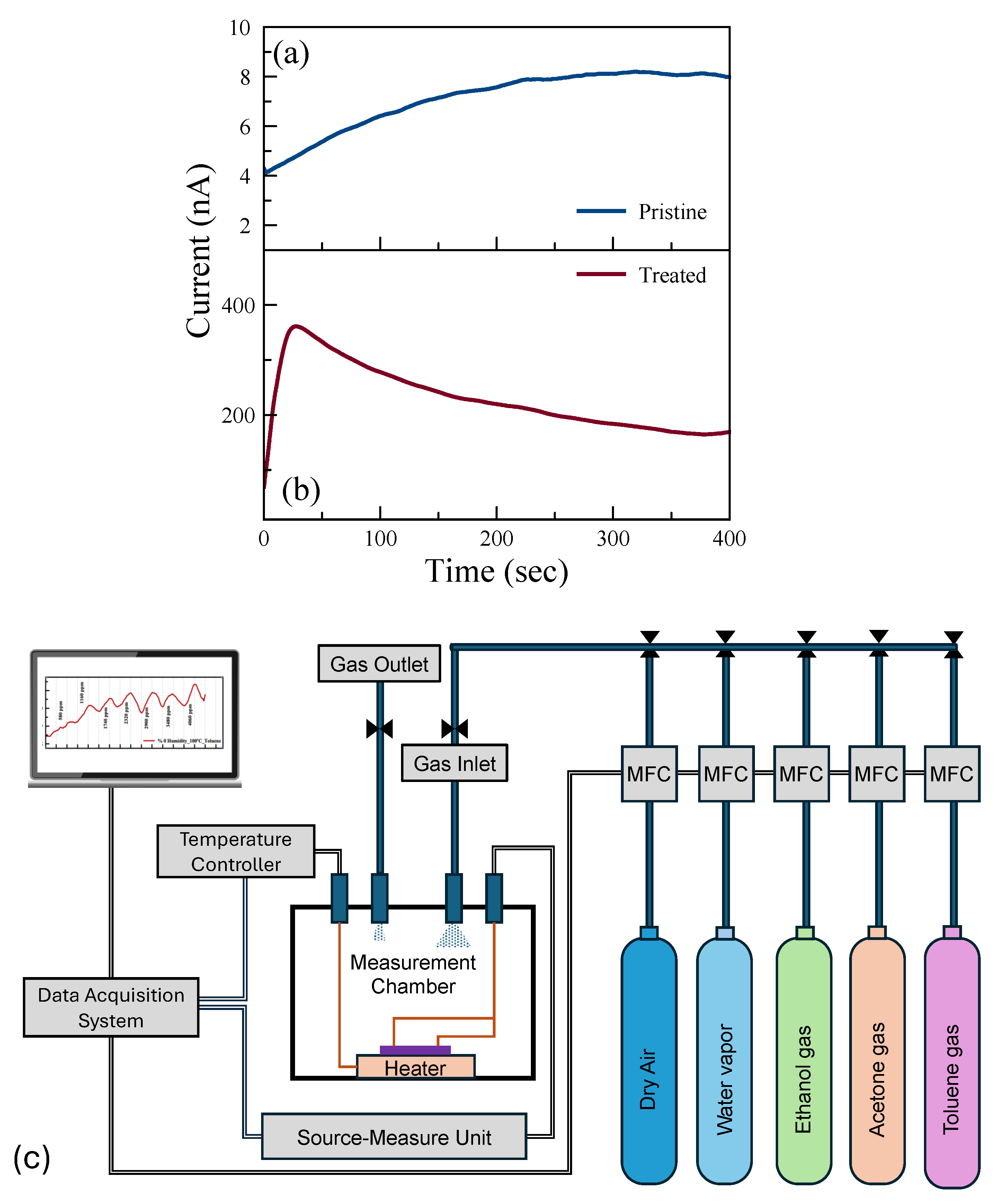
The VOC vapor was generated from cooled bubblers that were immersed in a thermally controlled bath, with synthetic air as the carrier gas. The gas stream saturated with the VOC analyte was then diluted with pure synthetic air to achieve the desired gas concentration. The total gas flow rate was set to 300 sccm by the computer-controlled mass flow controllers. The current–time characteristics of the gas sensors were measured under a constant bias of 1 V using a KEITHLEY 6517B Electrometer. A LakeShore 340 (Lake Shore Cryotronics, Westerville, OH, USA) temperature controller was used to control the ambient temperature. All the gas-sensing experiments were carried out by introducing the VOC target gas mixed with dry air for 10 min followed by a flow of pure dry air for 10 min in each cycle. Gas-sensing experiments were carried out by monitoring the current change of the sensors with a constant voltage supply (1 V). The response of the sensor was calculated based on the resistivity changes of the active material so that it could be compared independently of the device geometry (with different channel widths and lengths). The response is defined as R = where and represent the resistivities of the gas before and after contact with the sensor, respectively. The resistivity of the sensor is defined as , where R, w, and l represent resistance, contact width, and channel length, respectively [35].
3. Results and Discussion
3.1. Surface Characterization
We carried out WCA measurements and EFM imaging to characterize the surface of few-layer MoS2 before and after the UV-O3 treatment. Before the UV-O3 treatment, we observed that the WCAs are very different between a blank substrate (Borofloat® glass, 29° ± 2°) and a glass substrate covered with MoS2 flakes (78° ± 15°), as shown in Figure 1a,c, indicating that the blank glass substrate is much more hydrophilic than the MoS2 surface, which is consistent with the literature [36]. The large uncertainty in the WCA values originated from the variation in flake density over a large area of the sample. After a 4 min UV-O3 treatment, the WCA increased by 15% for the MoS2 sample (becoming slightly more hydrophobic) but decreased by 14% for the blank reference sample (slightly more hydrophilic); see Figure 1b,d. UV-O3 treatment is known to make glass surfaces more hydrophilic by introducing hydroxyl (OH) groups that attract water molecules. The mild increase in hydrophobicity on the MoS2 surface can be attributed to the oxidation of the surface [37,38].
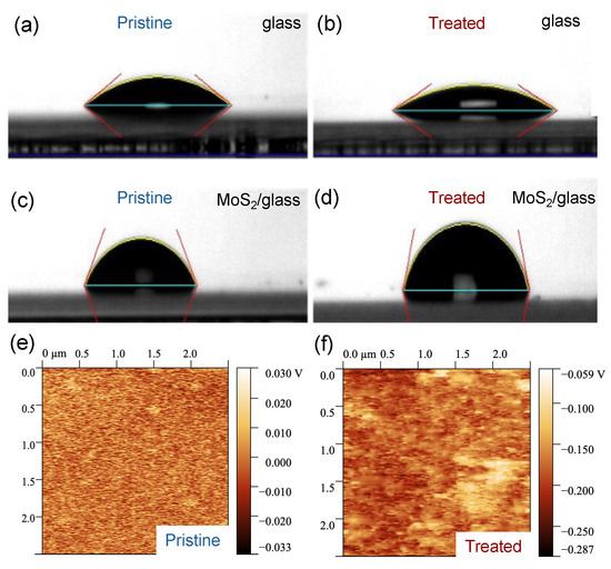
Figure 1.
Surface characterization before and after UV-O3 treatment. (a–d) The water contact angles (WCA) were measured on a blank Borofloat® glass and a Borofloat® glass with a high density of few-layer MoS2 flakes before (a,c) and after (b,d) a 4 min UV-O3 treatment, respectively; (e,f) are the electrostatic force microscopy (EFM) images of the 5 L MoS2 flake surface before and after UV-O3 treatment, respectively.
EFM is an electrical mode in AFM to map variations in the sample’s electric field and reveal information about the surface potential and charge distribution. The surface potential is obtained relative to the tip potential. In our EFM measurements, we kept the tip potential and the distance from the tip to the surface constant and obtained surface potential mapping and the average surface potential from the active region of the sensing devices. The average surface potential changes from 0.094 mV to −112.5 mV after a 4 min UV-O3 treatment; see Figure 1e,f. This reduction in the surface potential is due to the reduction in the Fermi level of the MoS2 flake, resulting in p-type characteristics [39].
3.2. Photoluminescence and Raman Spectroscopy of MoS2
The layer number of the flake was further confirmed based on the peak wavelength of the PL spectrum. A PL peak wavelength at 890 nm indicates that the flake is a five-layer (5 L) MoS2, see the highlighted area in Figure 2a (I). In our previous study, we observed that 4 min of UV-O3 exposure time was optimal to produce p-type-doped MoS2 while maintaining above 80% of the initial PL intensity [34]. Therefore, half of the active material was treated for 4 min while the other side was kept pristine under the resist, see Figure 2a (IV), in order to create two channels in the same material for sensing. Figure 2b,c show the PL and Raman spectra of the pristine and the UV-O3-treated MoS2, respectively. The PL spectra of two sides of the material were used as a control indicator of whether the UV-O3 treatment degraded the material or not. With maintaining 70% of the initial PL intensity, it can be concluded there is no structural degradation in the 4 min treated material. On the other hand, the comparison of the Raman spectra between the pristine and treated materials was used as an indicator if the treated material indeed turned into being p-type-doped. The Raman spectrum of MoS2 is characterized by two main vibration modes, E2g and A1g, representing the in-plane and out-of-plane vibrations, respectively [40]. It is known that the E2g mode is sensitive to the strain while the A1g vibration mode is sensitive to the doping effect [40,41,42]. Kang et al. and Shi et al., in different studies, showed that changes in the line width and blueshifts (toward the higher frequency) of the A1g vibration mode are indications of the p-type doping effect in MoS2 [41,43]. The Raman spectrum in Figure 2c shows 0.8 cm−1 of blueshift in the A1g vibration mode, which can be attributed to the p-type doping effect in MoS2. After the PL and Raman examinations, the electrodes were fabricated to achieve two sensing channels in the same device.
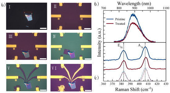
Figure 2.
(a) Optical microscope images (with a scale bar of 50 ) of the sensor in different fabrication steps: I. As-exfoliated few-layer MoS2 flake on polydimethylsiloxane (PDMS) with the 5-layer area highlighted with red dotted lines; II. Contact electrodes fabricated on SiO2-on-Si substrate with a 200 200 clear window for transferring 2D materials; III. After transferring the few-layer MoS2 flake onto SiO2-on-Si substrate; IV. After opening a window in the PMMA resist layer on half of the 5-layer MoS2 for the UV-O3 treatment, V. After patterning the electrode fingers to connect the MoS2 flake and the prefabricated contact pads in the MMA/PMMA resist; VI. Final device after metallization and lift-off process; (b) PL and (c) Raman spectra of the pristine (blue) and the UV-O3-treated (red) MoS2.
3.3. Sensing Performance
The current–time (I-t) characteristics were investigated to examine the saturation time, i.e., time before the current saturates with the applied voltage. Figure 3a,b show the room-temperature I-t characteristics of pristine and treated sensors, respectively. The p-type doping effect due to the UV-O3 treatment results in reduced contact resistance, and hence the measured current increases 50 times after the treatment. Although there is a difference in the magnitude of the current for these two sensing channels, the current saturates after 5 min of applied voltage in both channels. This saturation time was taken into consideration in the sensing experiments.

Figure 3.
Current–time (with a constant bias of 1 V applied) plots of (a) pristine and (b) UV-O3-treated MoS2, respectively, and (c) a schematic illustration of the gas measurement system.
Gas measurements were carried out with the following flow sequence, with the gas flow system illustrated in Figure 3c: 10 min flow of dry air, followed by 10 min flow of target gas mixed with dry air, and then 10 min flow of dry air followed by a flow of a different concentration of gas mixture. In this study, we aimed to show how post-growth functionalization of 2D materials can affect their gas-sensing performance. To understand the mechanism behind the change in performance, we eliminated all other environmental/external effects, such as 2D material layer thicknesses and humidity [44]. We examined the sensing performance at room temperature (RT) and 100 °C. The response of the sensors for each gas was measured with seven different concentrations in the range of 300 ppm and 15,000 ppm. The individual range was chosen based on their occupational environment gas exposure limit. Figure 4 shows the real-time monitoring of the current change of the pristine MoS2 gas sensor with varying gas concentrations at RT and 100 °C. While there is no response in the sensors for VOC gases at RT, reasonable responses were observed in the pristine sensor to ethanol, acetone, and toluene at 100 °C.
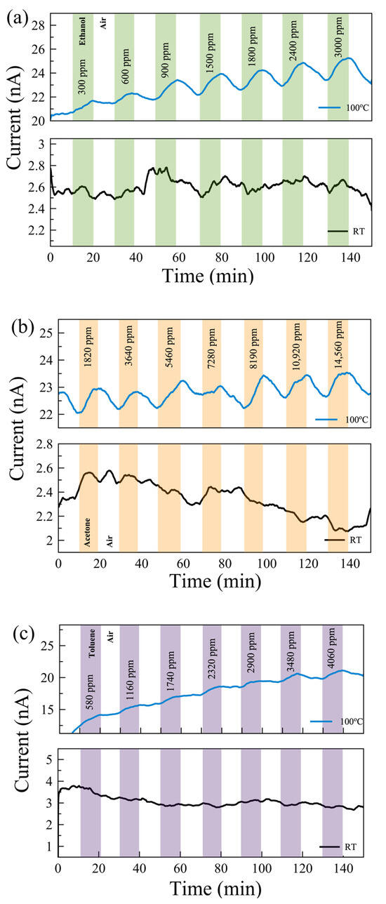
Figure 4.
Real-time monitoring of current change in a few-layer pristine MoS2-based gas sensor with varying gas concentrations of (a) ethanol, (b) acetone, and (c) toluene gases at 100 °C (top) and room temperature (RT, bottom).
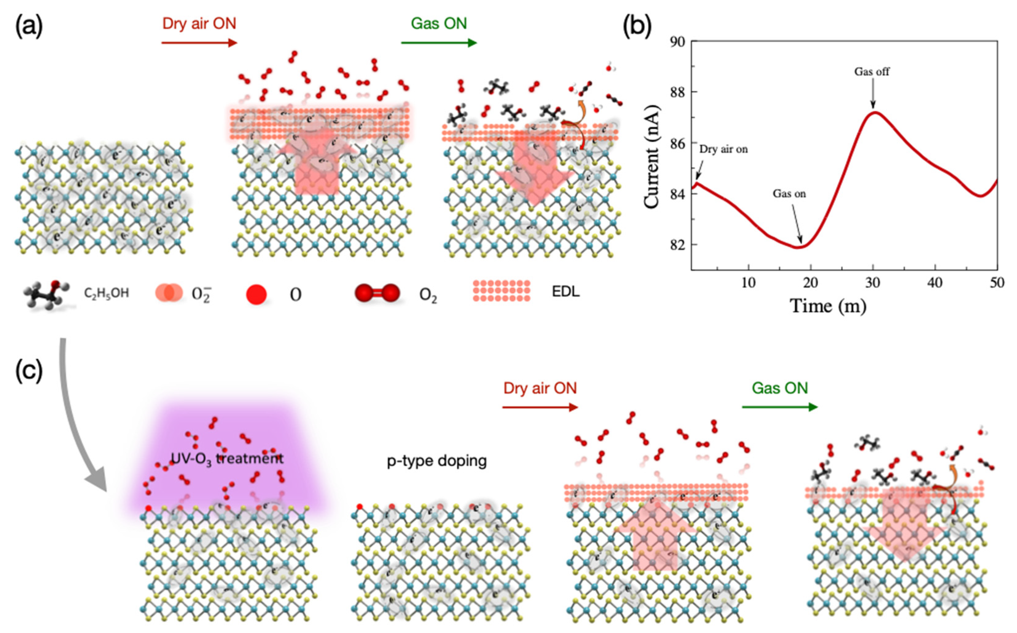
The pristine MoS2 used in this study is intrinsically n-doped. The main gas-sensing mechanism of the pristine MoS2 sensors is the same as any n-type bulk semiconductor-based sensor. In an n-type semiconductor where electrons are the majority charge carriers, the oxygen molecules in the air are physically adsorbed, by trapping free electrons, onto the surface, resulting in space charge layers that are called electron depletion layers (EDLs). Because the physically bonded oxygen reacts with sensing molecules and forms chemical bonds, the resistance of the sensor reduces. The types of chemisorbed ionized-oxygen species (O−, O2−, or O2−) are largely affected by the working temperature as seen in Equations (1)–(4) [45].
O2(gas)→O2(ads)
O2(ads) + e− → O2− (ads) (<150 °C)
O2− (ads) + e− → 2O− (ads) (150 °C–400 °C)
O− (ads) + e− → O2− (ads) (>400 °C)
When a pristine MoS2 sensor is operated at 100 °C, the O2− ion plays a more important role in detecting VOCs. The sensing mechanism in the pristine MoS2 sensor is illustrated in Figure 5.
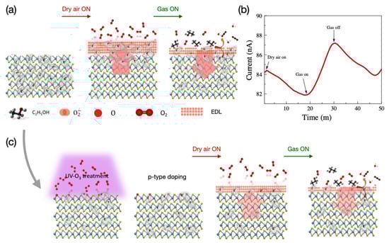
Figure 5.
(a) Illustration of the sensing mechanism, (b) response of the pristine MoS2-based gas sensor to dry air and ethanol gas at 100 °C, and (c) illustration of the sensing mechanism of UV-O3-treated sensor.
Ethanol, acetone, and toluene gases react with surface oxygen ions. The interaction mechanism of the chemical reactions at 100 °C is given by Equations (5)–(7) for ethanol, acetone, and toluene, respectively.
C2H5OH(g) + 3O2− (ads) →3H2O(g) + 2CO2(g) + 3e−
CH3COCH3(g) + 4O2− (ads) →3H2O(g) + 2CO2(g) + 4e−
C7H8(g) + 9O2− (ads) → 7CO2(g) + 4H2O(g) + 9e−
As a result of these reactions, different amounts of CO2, H2O, and numbers of electrons are generated with the presence of ethanol, acetone, and toluene, respectively. The removal of O2− ions from the surfaces due to reactions with the target gas, for example, ethanol, causes a thinner EDL region and a decrement in the potential barrier, which results in an increment in the sensor current as shown in Figure 6. The trend of different responses to different gases follows the amount of required O2− for each gas molecule; see Equations (5)–(7). Therefore, we can conclude that the response of the sensors was dependent on the thickness of EDLs [11,46].
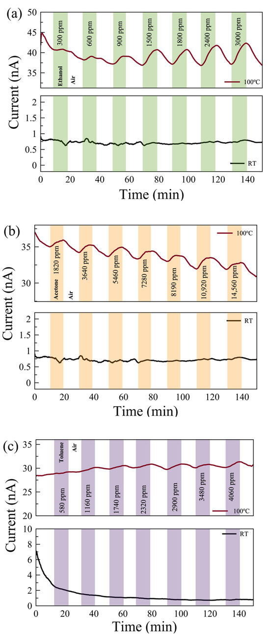
Figure 6.
The responses of UV-O3-treated few-layer MoS2 gas sensors exposed to (a) ethanol, (b) acetone, and (c) toluene gases at 100 °C (top) and at RT (bottom). The background drifts in the current values are due to the carriers stabilizing in the sensor.
Figure 6 shows the real-time monitoring of the current change in a few-layer UV-O3-treated MoS2 sensor with varying gas concentrations at RT and 100 °C. Reasonable responses are observed for ethanol and acetone at 100 °C compared to no notable response at RT. The limits of detection (LODs) are estimated to be <300 ppm, <1500 ppm, and <500 ppm for ethanol, acetone, and toluene, respectively. Characterizing the dual-channel sensors at a wider range of temperatures may offer further improvement in sensitivity and selectivity, which can be investigated in future work. The responses of the pristine few-layer MoS₂ sensors to 3000 ppm ethanol, acetone, and toluene gases at 100 °C are 18%, 3.5%, and 49%, respectively. The UV-O3-treated MoS₂ sensors show responses of 13.4%, 3.1%, and 6.7%, respectively. Therefore, such a dual-channel sensing device demonstrates a 7-fold improvement in selectivity for toluene against ethanol and acetone. Due to the toluene molecules requiring two to three times more O2− (ads) ions to react with compared to the ethanol and acetone molecules (see Equations (5)–(7)), the response to toluene gas is expected to be affected much more significantly by the different EDL layers formed on top of the active surface before and after the UV-O3 treatment compared to the other two gases, resulting in an enhanced selectivity for toluene.
It has been revealed that UV-O3 treatment leads to the formation of S-O bonds in the MoS2. The O− ions can also exist at interstitial sites and S-vacancies [47]. The physical and oxygen-mediated chemical bonds in the UV-O3-treated sensors result in a p-type characteristic in the MoS2. Therefore, UV-O3-treated sensors showed a reduced response to toluene compared to acetone and ethanol due to its large molecular structure and more ionized oxygen required to bind (Equation (7)). Figure 7 shows the comparison of the responses for the pristine and UV-O3-treated MoS2 sensors. The response of the UV-O3-treated sensor reduces for all VOCs except acetone at higher concentrations. This reduction is attributed to switching the type of the free carriers from electron-dominant to hole-dominant, resulting in a reduction in the dynamic EBL thickness of the sensor surface during the operation. To achieve a better resolution and higher sensitivity, a larger number of sensing channels can be pursued, inspired by the structure proposed by Rabchinskii et. al. [16], with large area flakes or wafer-scale MoS2 grown by chemical vapour deposition. Furthermore, the layer-thickness-dependent sensitivity can be explored in future studies.
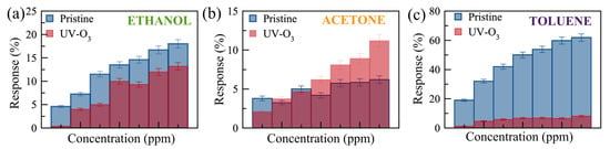
Figure 7.
Comparison of the responses to (a) ethanol (300 to 3000 ppm, with error bars of 5%), (b) acetone (1820–14,560 ppm, with error bars of 8%), and (c) toluene (580–4060 ppm, with error bars of 6%) gases for pristine (blue) and UV-O3-treated (red) few-layer MoS2 gas sensors. The error bars were obtained from the resistivity trends of 4 different devices.
4. Conclusions
We have designed and fabricated a few-layer MoS2-based dual-channel gas sensor platform for volatile organic compounds, including ethanol, acetone, and toluene. The multi-pixelated sensor platform consists of two sensors side by side made from the same material. While one-half of the material is kept as pristine, i.e., an electron-dominant sensor, the other half of the material is treated by UV-O3 to obtain a hole-dominant sensor. UV-O3 treatment is used to control the free electron density in the active material and change the thickness of the electron depletion layers. Other techniques such as oxygen plasma or annealing in air or an O2 environment can also be employed for the same purpose, but we believe that UV-O3 treatment is more reliable and reproducible. The responses of pristine MoS2 gas sensors to 3000 ppm of ethanol, acetone, and toluene gases were found to be 18%, 3.5%, and 49%, and those of UV-O3-treated sensors were 13.4%, 3.1%, and 6.7%, respectively, with 0% humidity at 100 °C. The proposed double-channel sensor system reveals excellent selectivity to toluene, which can be further integrated in future work.
Author Contributions
Conceptualization, F.S.; methodology, E.K., G.A., Y.K.B., C.T., Y.W. and F.S.; validation, A.E., Y.W. and F.S.; formal analysis, E.K., A.E., Y.W. and F.S.; investigation, E.K., G.A., C.T., Y.W. and F.S.; resources, C.T., A.E., Y.W. and F.S.; data curation, A.E., Y.W. and F.S.; writing—original draft preparation, E.K. and F.S.; writing—review and editing, A.E., Y.W. and F.S.; visualization, F.S.; supervision, Y.W. and F.S.; project administration, F.S.; funding acquisition, A.E., Y.W. and F.S. All authors have read and agreed to the published version of the manuscript.
Funding
This research was funded by the Royal Academy of Engineering (Research Fellowship awarded to Y.W., RF/201718/17131), the Scientific Research Projects Coordination Unit of Istanbul University (FBA-2023-39412, FBG-2022-38573, FBG-2021-37896), the Scientific and Technological Research Council of Turkey (TUBITAK) project (121F169).
Data Availability Statement
The authors declare that all the data and code supporting the findings of this study are available within the article, or upon request from the corresponding author.
Conflicts of Interest
The authors declare no conflict of interest.
References
- Kansal, A. Sources and Reactivity of NMHCs and VOCs in the Atmosphere: A Review. J. Hazard. Mater. 2009, 166, 17–26. [Google Scholar] [CrossRef] [PubMed]
- Peng, G.; Tisch, U.; Adams, O.; Hakim, M.; Shehada, N.; Broza, Y.Y.; Billan, S.; Abdah-Bortnyak, R.; Kuten, A.; Haick, H. Diagnosing Lung Cancer in Exhaled Breath Using Gold Nanoparticles. Nat. Nanotechnol. 2009, 4, 669–673. [Google Scholar] [CrossRef] [PubMed]
- Kim, N.H.; Choi, S.J.; Yang, D.J.; Bae, J.; Park, J.; Kim, I.D. Highly Sensitive and Selective Hydrogen Sulfide and Toluene Sensors Using Pd Functionalized WO3 Nanofibers for Potential Diagnosis of Halitosis and Lung Cancer. Sens. Actuators B Chem. 2014, 193, 574–581. [Google Scholar] [CrossRef]
- Zhao, Q.; Li, Y.; Chai, X.; Xu, L.; Zhang, L.; Ning, P.; Huang, J.; Tian, S. Interaction of Inhalable Volatile Organic Compounds and Pulmonary Surfactant: Potential Hazards of VOCs Exposure to Lung. J. Hazard. Mater. 2019, 369, 512–520. [Google Scholar] [CrossRef] [PubMed]
- Pinto, D.M.; Blande, J.D.; Souza, S.R.; Nerg, A.M.; Holopainen, J.K. Plant Volatile Organic Compounds (Vocs) in Ozone (O3) Polluted Atmospheres: The Ecological Effects. J. Chem. Ecol. 2010, 36, 22–34. [Google Scholar] [CrossRef] [PubMed]
- Mirzaei, A.; Leonardi, S.G.; Neri, G. Detection of Hazardous Volatile Organic Compounds (VOCs) by Metal Oxide Nanostructures-Based Gas Sensors: A Review. Ceram. Int. 2016, 42, 15119–15141. [Google Scholar] [CrossRef]
- Tomić, M.; Šetka, M.; Vojkůvka, L.; Vallejos, S. Vocs Sensing by Metal Oxides, Conductive Polymers, and Carbon-Based Materials. Nanomaterials 2021, 11, 552. [Google Scholar] [CrossRef] [PubMed]
- Xia, S.; Zhu, H.; Cai, H.; Zhang, J.; Yu, J.; Tang, Z. Hydrothermally Synthesized CuO Based Volatile Organic Compound Gas Sensor. RSC Adv. 2014, 4, 57975–57982. [Google Scholar] [CrossRef]
- Wang, N.; Zhou, Y.; Chen, K.; Wang, T.; Sun, P.; Wang, C.; Chuai, X.; Zhang, S.; Liu, X.; Lu, G. Double Shell Cu2O Hollow Microspheres as Sensing Material for High Performance N-Propanol Sensor. Sens. Actuators B Chem. 2021, 333, 129540. [Google Scholar] [CrossRef]
- Al-Hardan, N.H.; Abdullah, M.J.; Abdul Aziz, A.; Ahmad, H.; Low, L.Y. ZnO Thin Films for VOC Sensing Applications. Vacuum 2010, 85, 101–106. [Google Scholar] [CrossRef]
- Seekaew, Y.; Wisitsoraat, A.; Phokharatkul, D.; Wongchoosuk, C. Room Temperature Toluene Gas Sensor Based on TiO2 Nanoparticles Decorated 3D Graphene-Carbon Nanotube Nanostructures. Sens. Actuators B Chem. 2019, 279, 69–78. [Google Scholar] [CrossRef]
- Li, B.; Zhou, Q.; Peng, S.; Liao, Y. Recent Advances of SnO2-Based Sensors for Detecting Volatile Organic Compounds. Front. Chem. 2020, 8, 321. [Google Scholar] [CrossRef] [PubMed]
- Dong, H.; Liu, Y.; Li, G.; Wang, X.; Xu, D.; Chen, Z.; Zhang, T.; Wang, J.; Zhang, L. Hierarchically Rosette-like In2O3 Microspheres for Volatile Organic Compounds Gas Sensors. Sens. Actuators B Chem. 2013, 178, 302–309. [Google Scholar] [CrossRef]
- Jang, A.R.; Lim, J.E.; Jang, S.; Kang, M.H.; Lee, G.; Chang, H.; Kim, E.K.; Park, J.K.; Lee, J.O. Ag2S Nanoparticles Decorated Graphene as a Selective Chemical Sensor for Acetone Working at Room Temperature. Appl. Surf. Sci. 2021, 562, 150201. [Google Scholar] [CrossRef]
- Rabchinskii, M.K.; Sysoev, V.V.; Glukhova, O.E.; Brzhezinskaya, M.; Stolyarova, D.Y.; Varezhnikov, A.S.; Solomatin, M.A.; Barkov, P.V.; Kirilenko, D.A.; Pavlov, S.I.; et al. Guiding Graphene Derivatization for the On-Chip Multisensor Arrays: From the Synthesis to the Theoretical Background. Adv. Mater. Technol. 2022, 7, 2101250. [Google Scholar] [CrossRef]
- Rabchinskii, M.K.; Sysoev, V.V.; Varezhnikov, A.S.; Solomatin, M.A.; Struchkov, N.S.; Stolyarova, D.Y.; Ryzhkov, S.A.; Antonov, G.A.; Gabrelian, V.S.; Cherviakova, P.D.; et al. Toward On-Chip Multisensor Arrays for Selective Methanol and Ethanol Detection at Room Temperature: Capitalizing the Graphene Carbonylation. ACS Appl. Mater. Interfaces 2023, 15, 28370–28386. [Google Scholar] [CrossRef]
- Donarelli, M.; Ottaviano, L. 2D Materials for Gas Sensing Applications: A Review on Graphene Oxide, MoS2, WS2 and Phosphorene. Sensors 2018, 18, 3638. [Google Scholar] [CrossRef]
- Zheng, W.; Xu, Y.; Zheng, L.; Yang, C.; Pinna, N.; Liu, X.; Zhang, J. MoS2 Van Der Waals p–n Junctions Enabling Highly Selective Room-Temperature NO2 Sensor. Adv. Funct. Mater. 2020, 30, 435. [Google Scholar] [CrossRef]
- Kumar, S.; Mirzaei, A.; Kumar, A.; Hoon Lee, M.; Ghahremani, Z.; Kim, T.U.; Kim, J.Y.; Kwoka, M.; Kumar, M.; Sub Kim, S.; et al. Nanoparticles Anchored Strategy to Develop 2D MoS2 and MoSe2 Based Room Temperature Chemiresistive Gas Sensors. Coord. Chem. Rev. 2024, 503, 215657. [Google Scholar] [CrossRef]
- Jaiswal, J.; Das, A.; Chetry, V.; Kumar, S.; Chandra, R. NO2 Sensors Based on Crystalline MoSe2 Porous Nanowall Thin Films with Vertically Aligned Molecular Layers Prepared by Sputtering. Sens. Actuators B Chem. 2022, 359, 131552. [Google Scholar] [CrossRef]
- Wang, J.; Zeng, W.; Zhou, Q. Research Status of Gas Sensing Performance of MoTe2-Based Gas Sensors: A Mini Review. Front. Chem. 2022, 10, 950974. [Google Scholar] [CrossRef] [PubMed]
- Järvinen, T.; Lorite, G.S.; Peräntie, J.; Toth, G.; Saarakkala, S.; Virtanen, V.K.; Kordas, K. WS2 and MoS2 Thin Film Gas Sensors with High Response to NH3 in Air at Low Temperature. Nanotechnology 2019, 30, 405501. [Google Scholar] [CrossRef] [PubMed]
- Guo, R.; Han, Y.; Su, C.; Chen, X.; Zeng, M.; Hu, N.; Su, Y.; Zhou, Z.; Wei, H.; Yang, Z. Ultrasensitive Room Temperature NO2 Sensors Based on Liquid Phase Exfoliated WSe2 Nanosheets. Sens. Actuators B Chem. 2019, 300, 127013. [Google Scholar] [CrossRef]
- Afzal, A.M.; Iqbal, M.Z.; Dastgeer, G.; Nazir, G.; Mumtaz, S.; Usman, M.; Eom, J. WS2/GeSe/WS2 Bipolar Transistor-Based Chemical Sensor with Fast Response and Recovery Times. ACS Appl. Mater. Interfaces 2020, 12, 39524–39532. [Google Scholar] [CrossRef]
- Suh, J.M.; Shim, Y.S.; Kwon, K.C.; Jeon, J.M.; Lee, T.H.; Shokouhimehr, M.; Jang, H.W. Pd- and Au-Decorated MoS2 Gas Sensors for Enhanced Selectivity. Electron. Mater. Lett. 2019, 15, 368–376. [Google Scholar] [CrossRef]
- Chen, W.Y.; Yen, C.C.; Xue, S.; Wang, H.; Stanciu, L.A. Surface Functionalization of Layered Molybdenum Disulfide for the Selective Detection of Volatile Organic Compounds at Room Temperature. ACS Appl. Mater. Interfaces 2019, 11, 34135–34143. [Google Scholar] [CrossRef]
- Volatile Organic Compounds Emissions. Available online: https://www.epa.gov/sites/production/files/2018-07/documents/nei2014v2_tsd_05jul2018.pdf (accessed on 1 March 2024).
- Yan, H.; Song, P.; Zhang, S.; Yang, Z.; Wang, Q. Dispersed SnO2 Nanoparticles on MoS2 Nanosheets for Superior Gas-Sensing Performances to Ethanol. RSC Adv. 2015, 5, 79593–79599. [Google Scholar] [CrossRef]
- Singh, S.; Sharma, S. Temperature-Based Selective Detection of Hydrogen Sulfide and Ethanol with MoS2/WO3 Composite. ACS Omega 2022, 7, 6075–6085. [Google Scholar] [CrossRef] [PubMed]
- Verma, A.; Yadav, B.C. 2D/2D Nanostructured System Based on WO3/WS2 for Acetone Sensor and Breath Analyzer. ACS Appl. Nano Mater. 2023, 6, 5493–5507. [Google Scholar] [CrossRef]
- Hussain, A.; Lakhan, M.N.; Soomro, I.A.; Ahmed, M.; Hanan, A.; Maitlo, A.A.; Zehra, I.; Liu, J.; Wang, J. Preparation of Reduced Graphene Oxide Decorated Two-Dimensional WSe2 Nanosheet Sensor for Efficient Detection of Ethanol Gas. Physica E Low. Dimens. Syst. Nanostruct. 2023, 147, 115574. [Google Scholar] [CrossRef]
- Srivastava, S.; Singh, A.; Sahz, M.A.; Yadav, B.C.; Pandey, N.K. Development of V2O5@GO (1D/2D) Nanohybrid Based Chemiresistor for Low-Trace of Toluene. Sens. Actuators B Chem. 2024, 400, 134817. [Google Scholar] [CrossRef]
- Jamnani, S.R.; Moghaddam, H.M.; Leonardi, S.G.; Neri, G.; Ferlazzo, A. VOCs Sensing Properties of Samarium Oxide Nanorods. Ceram. Int. 2024, 50, 403–411. [Google Scholar] [CrossRef]
- Sarcan, F.; Armstrong, A.J.; Bostan, Y.K.; Kus, E.; McKenna, K.P.; Erol, A.; Wang, Y. Ultraviolet-Ozone Treatment: An Effective Method for Fine-Tuning Optical and Electrical Properties of Suspended and Substrate-Supported MoS2. Nanomaterials 2023, 13, 3034. [Google Scholar] [CrossRef] [PubMed]
- Sarcan, F. ZnO Nanoparticles-Based Vacuum Pressure Sensor. Nanotechnology 2020, 31. [Google Scholar] [CrossRef]
- Kozbial, A.; Gong, X.; Liu, H.; Li, L. Understanding the Intrinsic Water Wettability of Molybdenum Disulfide (MoS2). Langmuir 2015, 31, 8429–8435. [Google Scholar] [CrossRef]
- Jung, C.; Yang, H.I.; Choi, W. Effect of Ultraviolet-Ozone Treatment on MoS2 Monolayers: Comparison of Chemical-Vapor-Deposited Polycrystalline Thin Films and Mechanically Exfoliated Single Crystal Flakes. Nanoscale Res. Lett. 2019, 14, 278. [Google Scholar] [CrossRef]
- Sovizi, S.; Angizi, S.; Ahmad Alem, S.A.; Goodarzi, R.; Taji Boyuk, M.R.R.; Ghanbari, H.; Szoszkiewicz, R.; Simchi, A.; Kruse, P. Plasma Processing and Treatment of 2D Transition Metal Dichalcogenides: Tuning Properties and Defect Engineering. Chem. Rev. 2023, 123, 13869–13951. [Google Scholar] [CrossRef] [PubMed]
- Kim, C.J.; Lee, D.; Lee, H.S.; Lee, G.; Kim, G.S.; Jo, M.H. Vertically Aligned Si Intrananowire P-n Diodes by Large-Area Epitaxial Growth. Appl. Phys. Lett. 2009, 94, 173105. [Google Scholar] [CrossRef]
- Iqbal, M.W.; Shahzad, K.; Akbar, R.; Hussain, G. A Review on Raman Finger Prints of Doping and Strain Effect in TMDCs. Microelectron. Eng. 2020, 219, 111152. [Google Scholar] [CrossRef]
- Shi, Y.; Huang, J.K.; Jin, L.; Hsu, Y.T.; Yu, S.F.; Li, L.J.; Yang, H.Y. Selective Decoration of Au Nanoparticles on Monolayer MoS2 Single Crystals. Sci. Rep. 2013, 3, 1839. [Google Scholar] [CrossRef]
- Sarcan, F.; Fairbairn, N.J.; Zotev, P.; Severs-Millard, T.; Gillard, D.J.; Wang, X.; Conran, B.; Heuken, M.; Erol, A.; Tartakovskii, A.I.; et al. Understanding the Impact of Heavy Ions and Tailoring the Optical Properties of Large-Area Monolayer WS2 Using Focused Ion Beam. NPJ 2D Mater. Appl. 2023, 7, 23. [Google Scholar] [CrossRef]
- Kang, D.H.; Shim, J.; Jang, S.K.; Jeon, J.; Jeon, M.H.; Yeom, G.Y.; Jung, W.S.; Jang, Y.H.; Lee, S.; Park, J.H. Controllable Nondegenerate P-Type Doping of Tungsten Diselenide by Octadecyltrichlorosilane. ACS Nano 2015, 9, 1099–1107. [Google Scholar] [CrossRef] [PubMed]
- Yang, H.; Cai, S.; Wu, D.; Fang, X. Humidity-Dependent Characteristics of Few-Layer MoS2 Field Effect Transistors. Adv. Electron. Mater. 2020, 6, 659. [Google Scholar] [CrossRef]
- Hermawan, A.; Asakura, Y.; Inada, M.; Yin, S. One-Step Synthesis of Micro-/Mesoporous SnO2 Spheres by Solvothermal Method for Toluene Gas Sensor. Ceram. Int. 2019, 45, 15435–15444. [Google Scholar] [CrossRef]
- Mirzaei, A.; Kim, J.H.; Kim, H.W.; Kim, S.S. Resistive-Based Gas Sensors for Detection of Benzene, Toluene and Xylene (BTX) Gases: A Review. J. Mater. Chem. C Mater. 2018, 6, 4342–4370. [Google Scholar] [CrossRef]
- Burman, D.; Ghosh, R.; Santra, S.; Kumar Ray, S.; Kumar Guha, P. Role of Vacancy Sites and UV-Ozone Treatment on Few Layered MoS2 Nanoflakes for Toxic Gas Detection. Nanotechnology 2017, 28, 435502. [Google Scholar] [CrossRef]


Disclaimer/Publisher’s Note: The statements, opinions and data contained in all publications are solely those of the individual author(s) and contributor(s) and not of MDPI and/or the editor(s). MDPI and/or the editor(s) disclaim responsibility for any injury to people or property resulting from any ideas, methods, instructions or products referred to in the content. |
© 2024 by the authors. Licensee MDPI, Basel, Switzerland. This article is an open access article distributed under the terms and conditions of the Creative Commons Attribution (CC BY) license (https://creativecommons.org/licenses/by/4.0/).