Abstract
We analyze theoretically an InGaN/GaN n-i-p diode with a single quantum well supporting only one bound state. The bottom parts of the diode, namely the first barrier and the quantum well, are heavily n-doped with silicon at 5 × 1019 cm−3 to ensure a high electron concentration in the well. The voltage drop in the diode occurs in the second AlGaN barrier, which is undoped, and structure ends with a p-doped GaN. The band structure of the diode is calculated by a Schrodinger–Poisson drift-diffusion solver. Next, we calculate the absorption from the bound state in the well to the “continuum” above the well. We show the oscillatory behavior of the spectrum, with the amplitude decreasing with more negative voltage applied to the diode. Oscillations are due to interferences of the wavefunctions between the edges of the well and the slope of the potential barrier.
1. Introduction
Intersubband transitions in quantum wells form the basis of Quantum Well Infrared Photodetectors (QWIPs) and Quantum Cascade Lasers, operating in the infrared [1]. These transitions occur for TM polarized light (perpendicular to the plane of the well so the samples require special preparation). For wider wells (supporting several bound states), the dominant transition is usually from the ground state to the first excited state. For narrow wells supporting only one bound state, the transitions to the continuum above the well become important. There is a rich literature describing the “above-barrier resonances” in various GaInAs/AlGaAs structures for wells close to the surface of the sample [2,3], double-barrier quantum wells [4,5] etc. These resonances occur due to interference of the continuum wavefunctions reflected from different potential discontinuities. Another class of “above barrier resonances” can be created by the presence of an electric field in the barrier. Electroabsorption in narrow GaAs quantum wells has been theoretically discussed in Refs. [6,7], and some experimental results were shown in Ref. [8]. The difficulties with experimental observation of the above-barrier electroabsorption resonances in arsenide structures were related to a fairly small effective mass of electrons (0.067m0 for GaAs), relatively weak fields (10–40 kV/cm) required for strong resonances, and wide barriers (over 50 nm) required between the wells. Since the rapid development of nitride devices, there have been many investigations of intersubband transitions, first in GaN/AlGaN quantum wells [9,10,11,12] and later in InGaN/GaN quantum wells [13,14,15]. The effective mass of electrons is much higher in nitrides (0.2m0 in GaN) and very strong electric fields can appear both in the wells and in the barriers (a few MV/cm). On the other hand, nitride quantum wells suffer from composition and width fluctuations which lead to much broader linewidths, both in the interband and in intersubband transitions. However, relatively narrow linewidths in intersubband absorption (38 meV) have been reported for GaN/AlGaN structures grown on nonpolar substrates [16].
In the present paper, we propose an n-i-p diode structure with a narrow InGaN quantum well (heavily doped) and with a strong electric field in the undoped barrier. This design provides much better conditions for observing absorption resonances than a quantum well in an external electric field. We calculate the potential profile of the structure under different external voltages using a one-dimensional drift-diffusion solver. The applied voltage allows us to tune the electric field in the undoped AlGaN barrier. Then, we calculate the absorption spectra from the ground state to the “continuum” above the quantum well. These spectra reveal the above-barrier resonances whose height and spacing changes with the applied voltage.
2. The Sample and Computational Methods
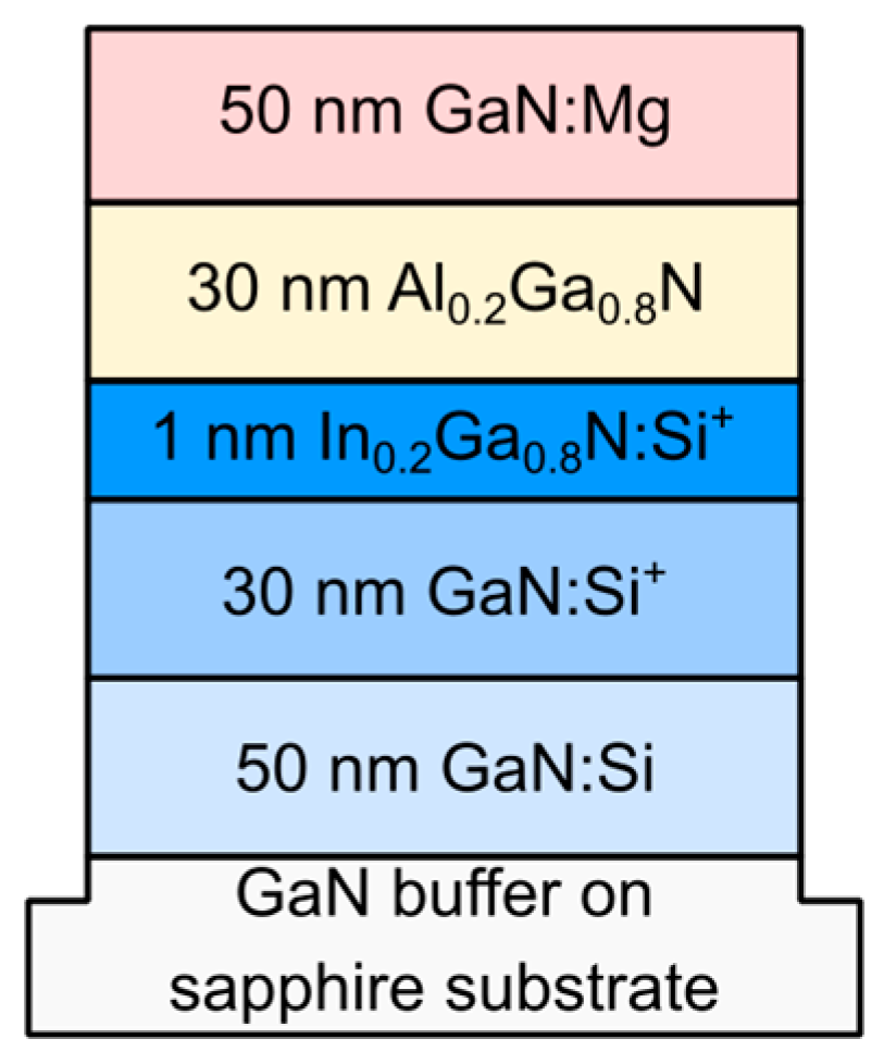
The schematic structure of proposed diode is shown in Figure 1. The structure starts with a 50 nm wide GaN:Si layer doped at 5 × 1018 cm−3. Next, a 30 nm GaN barrier and 1 nm In0.2Ga0.8N quantum well are placed, both heavily n-type doped at 5 × 1019 cm−3. Subsequently, there is an undoped Al0.2Ga0.8N barrier (undoped, 30 nm wide) followed by 50 nm p-type GaN:Mg doped at 5 × 1018 cm−3. All the layers are assumed to be coherently strained and lattice-matched to GaN. The InGaN well is subject to about 1.8% in-plane compressive strain. The AlGaN barrier is subject to 0.5% in-plane tensile strain. The structure is set to be Ga-polar (0001), resulting in the formation of polarization charges at the interfaces. The diode can be grown on a sapphire substrate with a few micrometer thick GaN buffer layer, and then the p-type and n-type contacts are placed on top to enable the diode to be polarized by the external voltage. However, this voltage is kept below the turn-on voltage of the diode, thus we do not expect the device to heat up due to high current flow. Moreover, we do not expect significant heating of the diode during illumination by an infrared light, if placed on a proper heatsink.
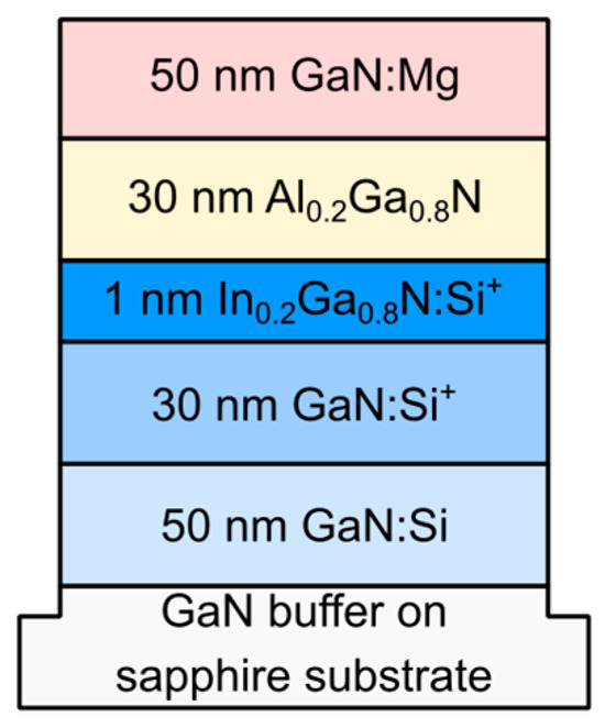
Figure 1.
Composition and doping profile of our proposed diode.
The band structure and potential profile of the proposed n-i-p diode has been calculated with a one-dimensional Poisson–Schrodinger solver developed by Wu [17,18]. The Poisson equation which has been numerically solved (together with the Schrodinger equation) is as follows:
where εr(z) is the relative dielectric permittivity, V(z) is the potential that is calculated as a result of successive iterations, and ρ(z) is the charge distribution in the structure. The charge distribution function is calculated from the electron density and the distribution of donors and acceptors in the structure. In simulations, we chose silicon (Si) as a donor and magnesium (Mg) as an acceptor for doping. The activation energies of those dopants are 25 meV for Si and 180 meV for Mg, respectively. The default material database has been used based on Refs. [19,20,21], and crucial material parameters can be found in Supplementary Materials.
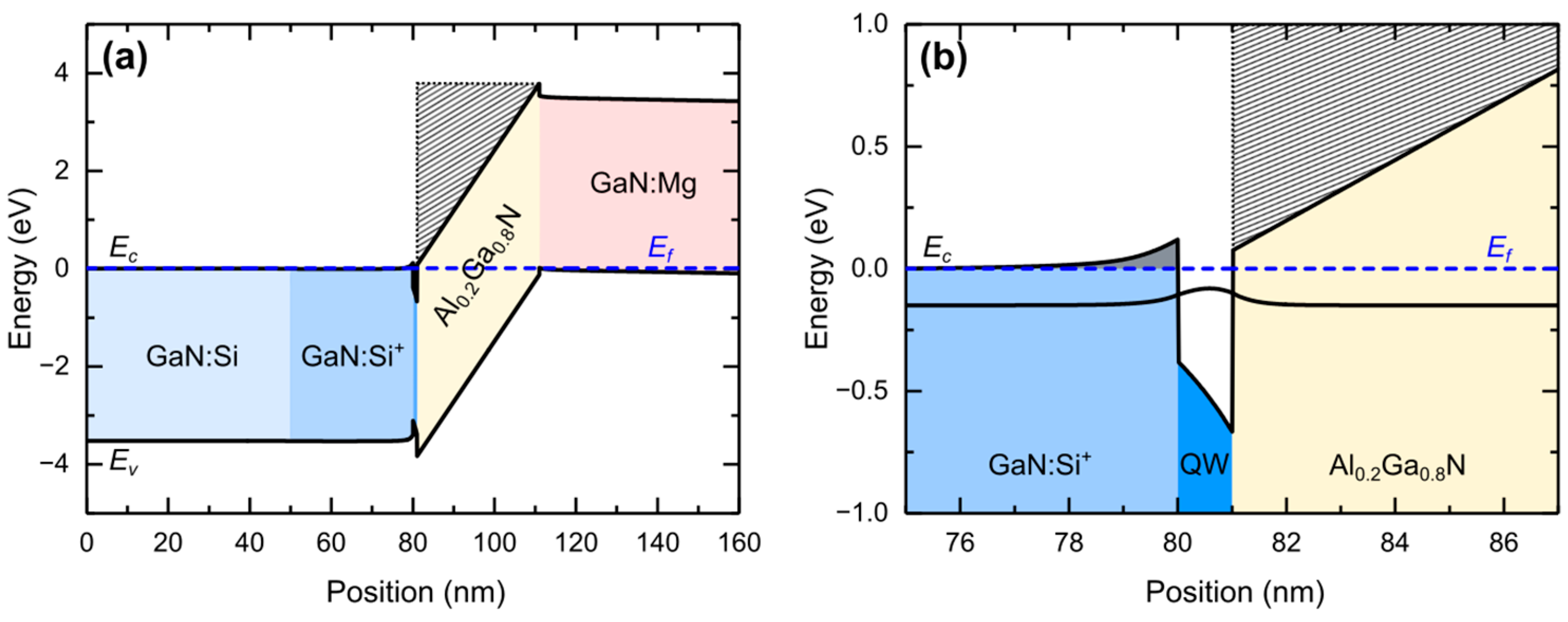
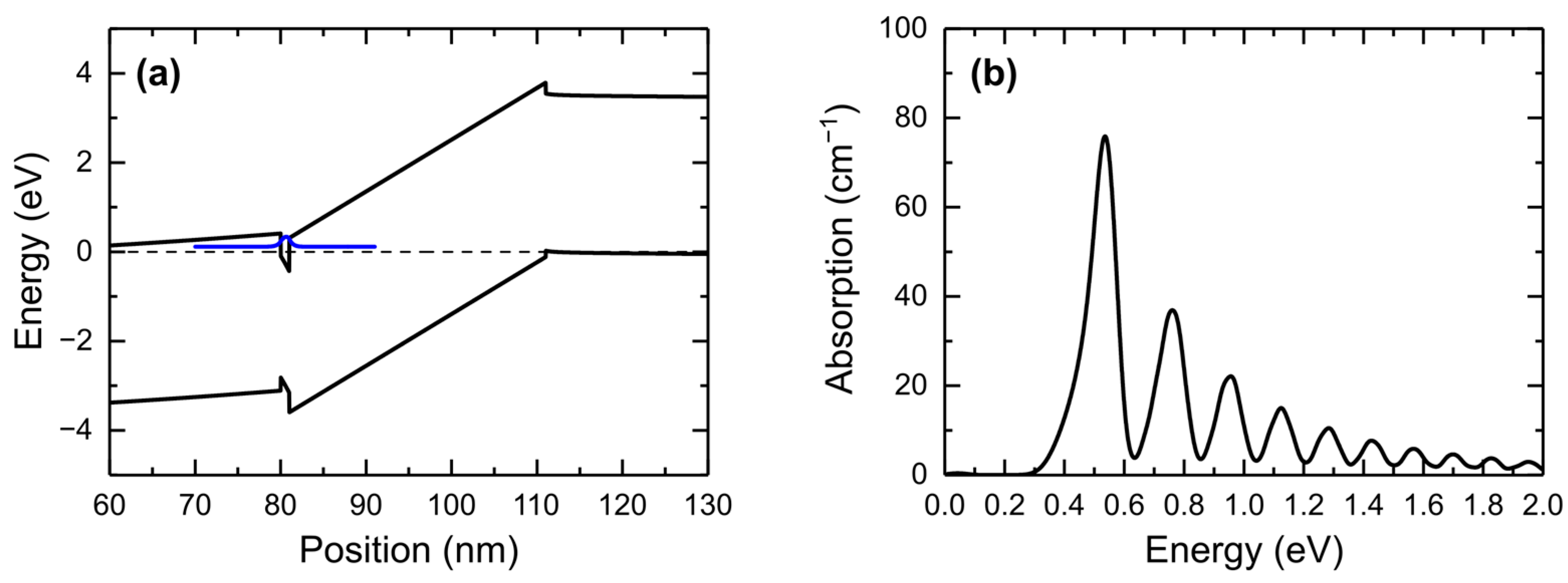
The band structure calculated for V = 0 V is shown in Figure 2a. The expanded region of the quantum well and barriers is shown in Figure 2b. Due to heavy doping in the left barrier and in the well, the built-in voltage of the n-i-p junction is mainly deposited in the undoped (right-hand) AlGaN barrier. The two-dimensional concentration of electrons in the well is determined as 8 × 1012 cm−2.

Figure 2.
(a) Band structure profile of the diode at 0 V obtained from the simulation and (b) expanded region of the quantum well and barriers. The Fermi level Ef is shown with dashed blue line. The hatched region above the right-hand barrier creates a triangular “well” which is the source of resonances in the “continuum”. The small barrier on the left-hand side (shown in grey color) perturbs the onset of “continuum”. The probability density of the ground state is shown in (b).
The idea leading to the choice of the above structure was to have a quantum well with only one bound state and the “continuum” for E > 0. In fact, the “continuum” in our structure is not infinite but bound in space by the buffer layer and the sapphire substrate. Therefore, we place an infinite barrier at z = 0 in Figure 2 so that the “continuum” extends between this barrier and the slope of the right-hand AlGaN barrier. The extension of the energy range of the “continuum” is limited by the height of the right-hand barrier in Figure 2, so it decreases with increasing positive bias. As it turns out, the results do not change if the infinite barrier is placed at z = 0, 10, 20, or 30 nm. Therefore, to speed up calculations, the infinite barrier was set at z = 30 nm. The additional barrier on the left-hand side of the well (colored in grey in Figure 2b in between 78 and 80 nm) perturbs the continuum but it is relatively small.
To calculate the absorption from the ground state to the continuum, we take into account the region between z = 30 and z = 110 nm. In this region, the Schrodinger equation (with the Duke Hamiltonian [22]) is solved numerically using the algorithm described in [23]:
where m(z) is the effective mass along the z direction, and V(z) is the potential obtained from the one-dimensional Poisson–Schrodinger solver. After calculating the wavefunctions, it is possible to determine the absorption using the Fermi golden rule as follows:
with , where e is the electron charge, is the refractive index, and is the matrix element corresponding to the transition between state i and state j. Similar calculation can be found in Refs. [24,25,26]. In the case of the intersubband transitions, the matrix element is nonzero for polarization along z, as follows:
In the considered case, the only occupied state is the ground state in the well, so the transitions are calculated from the state i = 1 to the excited states j > 1. In the plane of the quantum well, the states are plane waves (labeled by wavevector k) with parabolic dispersion, as shown in the following:
where m is the effective mass taken as 0.15m0 for the ground state (in the In0.2Ga0.8N well) and as 0.21m0 for the continuum states (which are mainly localized in the GaN barrier). This means that the transition energy depends on k and the summation over k states involves different one-dimensional states in the continuum.
The occupation of the ground state is governed by the Fermi function as follows:
where is the Fermi level, kB is the Boltzmann constant, and T is the temperature. We introduce level broadening [26,27,28] (caused by composition and width fluctuations in an InGaN well) by replacing delta function in Equation (3) with a Gaussian of a 40 meV half-width. We neglect the many-body effects [29,30,31,32], and we do not employ advanced DFT calculations [33,34]. Many-body effects due to Coulomb interactions (like excitonic effects) typically lead to corrections on the order of 10 meV, especially in the presence of a strong electric field in the well. In the presented scenario, electron–electron interactions can be omitted without significant impact. While the many-body effects may modify the absorption values, they do not alter the overall shape and the calculated position of absorption/gain curves [30]. Calculations excluding many-body effects remain in good agreement with the experimental results [35]. The many-body effects can induce excitonic phenomena [36] or other quasi-particle interactions such as polaritons [37] and plasmons [38], which significantly affect absorption spectra in two-dimensional materials or other non-classical semiconductors. However, in narrow InGaN quantum wells [29], these effects are small. As demonstrated in the next section, the absorption spectrum in our structure exhibits broad (100 meV) peaks due to the oscillatory behavior of the matrix elements. Under such conditions, the influence of electron–electron interactions (typically in the range of 10 meV) can be confidently disregarded.
3. Results
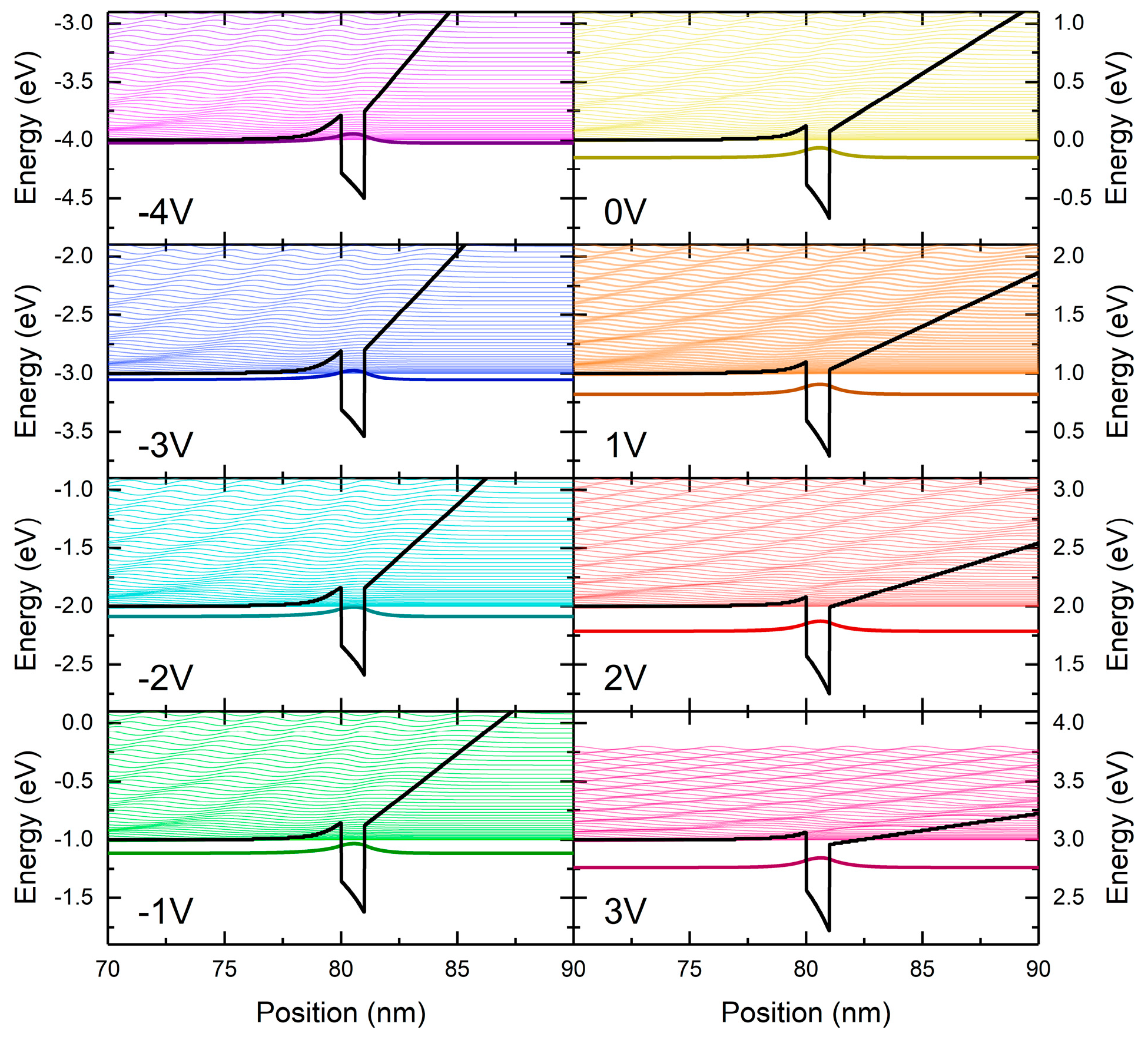
The band structure profile shown in Figure 2 was used as input for calculating eigenstates, both within the well and in the continuum above it. An infinite barrier was added at z0 to obtain discrete states in the continuum, and we normalized them within this “box.” For the z0 values of 30 nm and below, the absorption spectra do not change significantly. Therefore, we chose z0 = 30 nm to achieve a reliable continuum simulation with not too many eigenstates (for numerical reasons). For z0 = 30 nm, the calculation of eigenstates and eigenfunctions was performed in the range within the continuum above the well determined by the AlGaN barrier. Some of the calculated wavefunctions are shown in Figure 3 for voltages from −4 V to 3 V applied to the diode. The field in the well increases while the field in the right barrier decreases with increasing voltage. Accordingly, the distance from the ground state to the onset of the continuum increases.
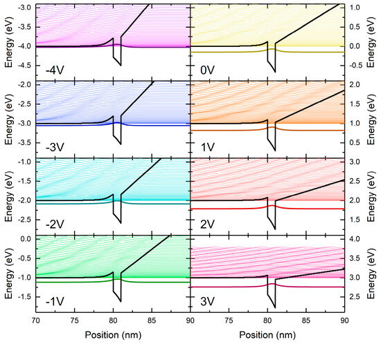
Figure 3.
The conduction band profile and the wavefunctions for different voltages applied to the diode. At 3 V, the “continuum” range above the well is reduced.
The absorption spectra for different voltages applied to the diode are shown in Figure 4. We observe a series of peaks, with decreasing separation and width with increasing voltage. The continuum range decreases for positive voltages since it is limited by the energy range corresponding to the right-hand barrier (see Figure 1). This is why we present the results up to V = 2 V since, as can be seen in Figure 3, the “continuum” range for V = 3 V becomes reduced (below 1 eV).
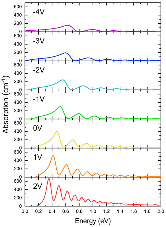
Figure 4.
Absorption spectra of the diode for different applied voltages.
In order to understand the origin of the spectra in Figure 4, we calculated separately the momentum matrix element (given in Equation (4)) and the density of the states measured from the ground state to the continuum. These are the two main factors affecting the absorption spectrum (Equation (3)). To facilitate comparison, the momentum matrix element and the density of states were normalized to dimensionless values by dividing them by their maximum value within the given range. These two quantities are presented as a function of the transition energy from the ground state to a given state in the “continuum”. The density of the states was calculated as the sum of the contributions from the individual transitions, which were defined as δ functions in Equation (3) and broadened to become Gaussians with a 40 meV half-width. The results are shown in Figure 5. The momentum matrix element (red lines) oscillates, and its maxima approach the continuum edge with increasing voltage. The maxima of the matrix element correspond approximately to bound states in the triangular well shown in Figure 2, i.e., the triangular quantum well with an infinite left-hand barrier and linear potential slope as the right-hand barrier (shown by bars in Figure 5). The downward shift of the red maxima with increasing voltage is simply due to the lowering of bound states in a triangular well with decreasing field. The density of states (black line) moves in the opposite direction with increasing bias, since the binding energy of the ground state increases with increasing bias (Figure 3). The absorption spectrum is dominated by the shift in the momentum matrix element, while the density of states produces the low-energy “tail” in the spectrum. Therefore, the resonances in the continuum are due to interferences of the wavefunctions reflected by the potential discontinuities at the edges of the quantum well and the reflection from the right-hand barrier. In order to increase the potential discontinuity at the right-hand edge of the well, we chose to have an AlGaN barrier in our diode.
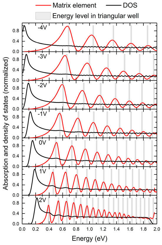
Figure 5.
Momentum matrix element (red lines) and density of states (black lines) as a function of energy (calculated from the energy of the ground state) for different voltages applied to the diode. Bars show the position of bound states in a triangular “well” denoted in Figure 1.
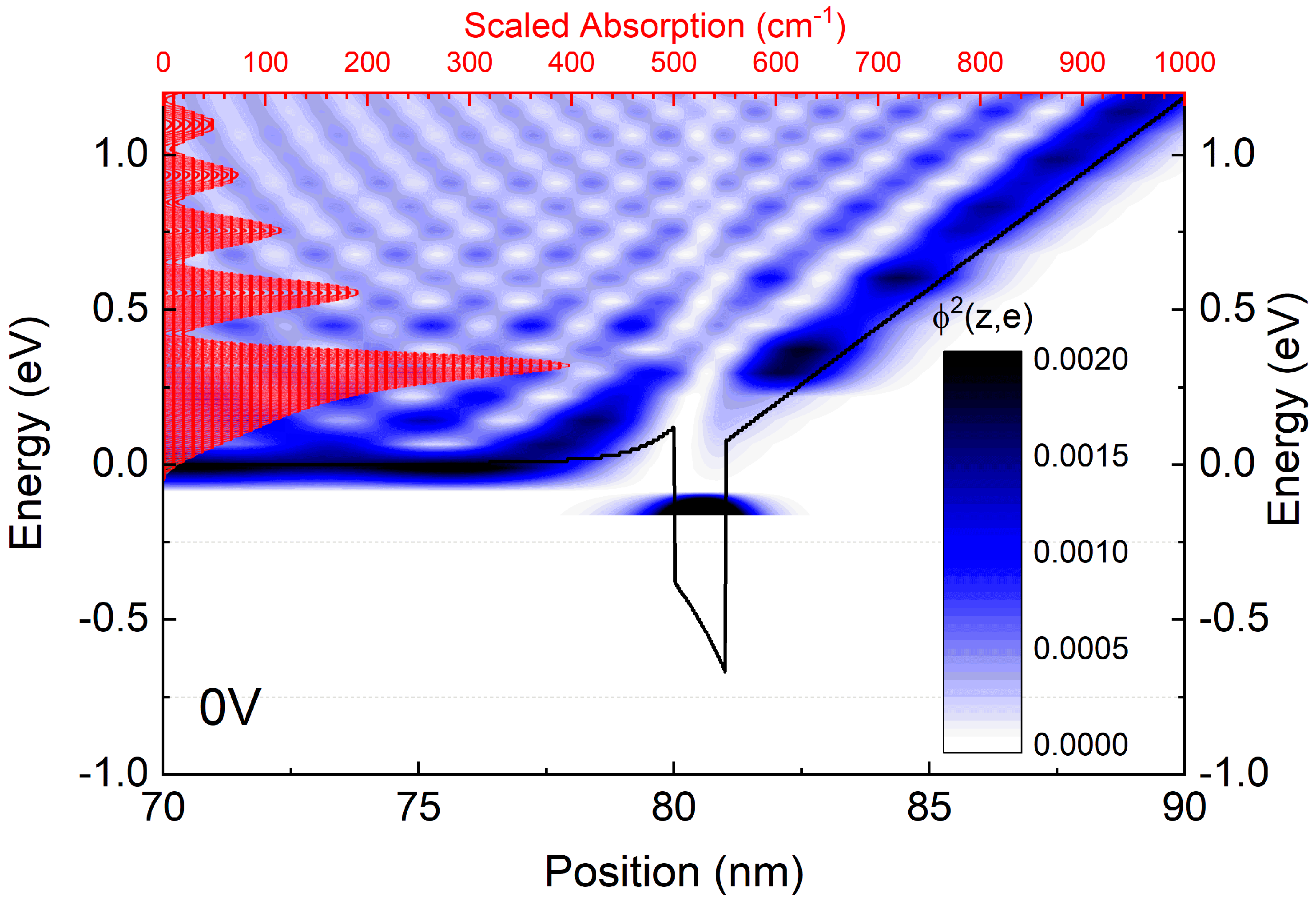
Figure 6 illustrates the probability density Φ2 plotted within the band profile for electrons in the case of V = 0. The probability is depicted using a color gradient from white through blue to black, depending on position and energy. The highest probability is observed within the quantum well. In the continuum, several regions within the triangular well exhibit increased probability. This result is compared with the previously calculated absorption, shown in red on the same figure as a bar chart. The absorption was rescaled (accounting for the difference from the ground state) to demonstrate that the transitions to the continuum correspond to the regions with the highest probability.

Figure 6.
The probability density, shown as a color map depending on position and energy, calculated for V = 0. The black line represents the conduction band profile, while the red bar chart displays the rescaled absorption coefficient.
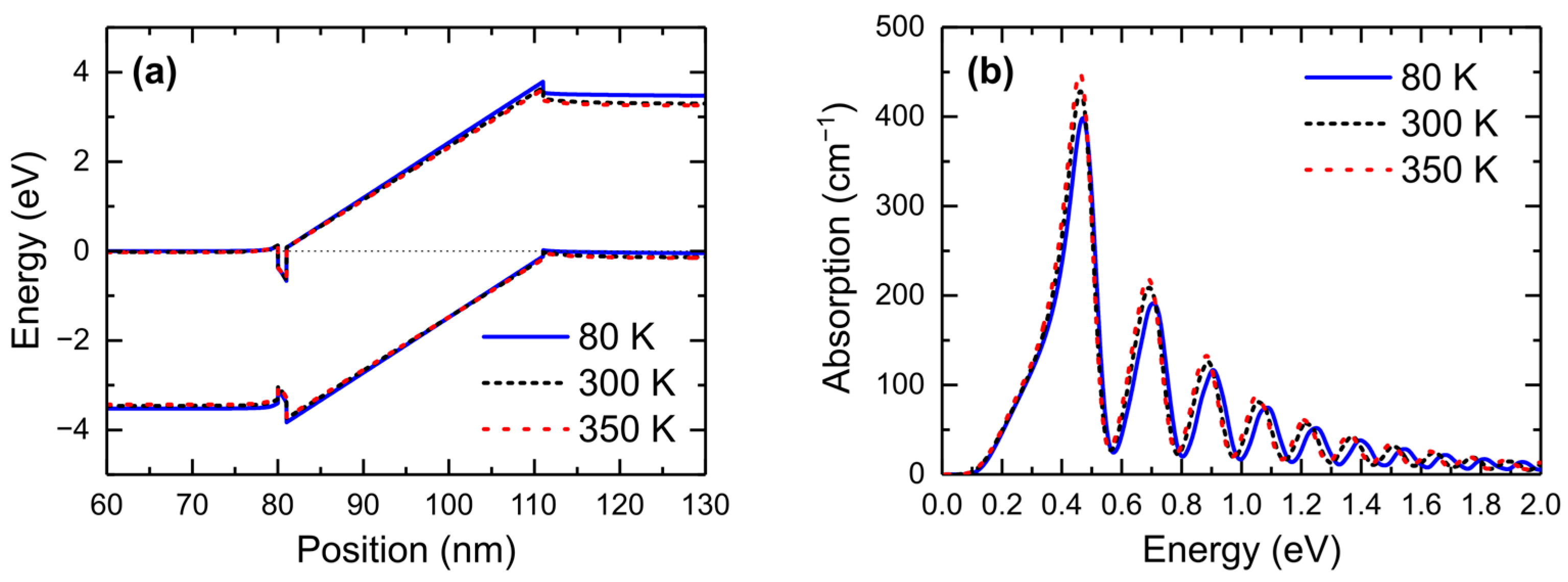
In the next step, we calculated the band structure and absorption spectra for V = 0 at the following three different temperatures: T = 80 K, T = 300 K, and T = 350 K (Figure 7). The three spectra turned out to be almost identical. This is because the dominant factor determining the broadening of the spectra is the momentum matrix element (given in Equation (4)) as can be seen by comparing Figure 4 and Figure 5. This implies that the possible heating of the sample by the light beam would not affect the oscillations in absorption.
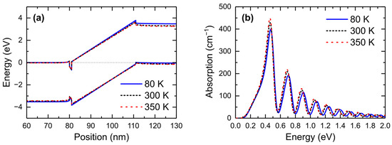
Figure 7.
(a) Band structure and (b) absorption spectra of n-i-p diode at 0 V and 80 K, 300 K, and 350 K, respectively.
Our proposed diode structure assumes very heavy doping in the left barrier and in the well. We checked the effect of much lower Si doping, namely 1017 cm−3 both in the left-hand barrier and in the quantum well. The potential profile and absorption spectra are shown in Figure 8. The left barrier becomes tilted and the concentration of electrons in the well is much lower than for the 1019 cm−3 doping. The oscillations are similar in terms of the period and width of the peaks, but the amplitude is about six times lower.
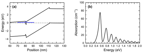
Figure 8.
(a) Band structure and (b) absorption spectra of structure with Si doping at 1017 cm−3 in the quantum well and left-hand side barrier at 80 K and 0 V. The square of the bound state wave function in the quantum well is marked with a blue line.
The additional calculation in the case of a nonpolar structure did not show absorption oscillations since the ground state in the well became resonant, so the electrons were not truly bound. Perhaps a deeper well (by increasing the indium content) or even more doping is needed to bind the ground state in a nonpolar quantum well.
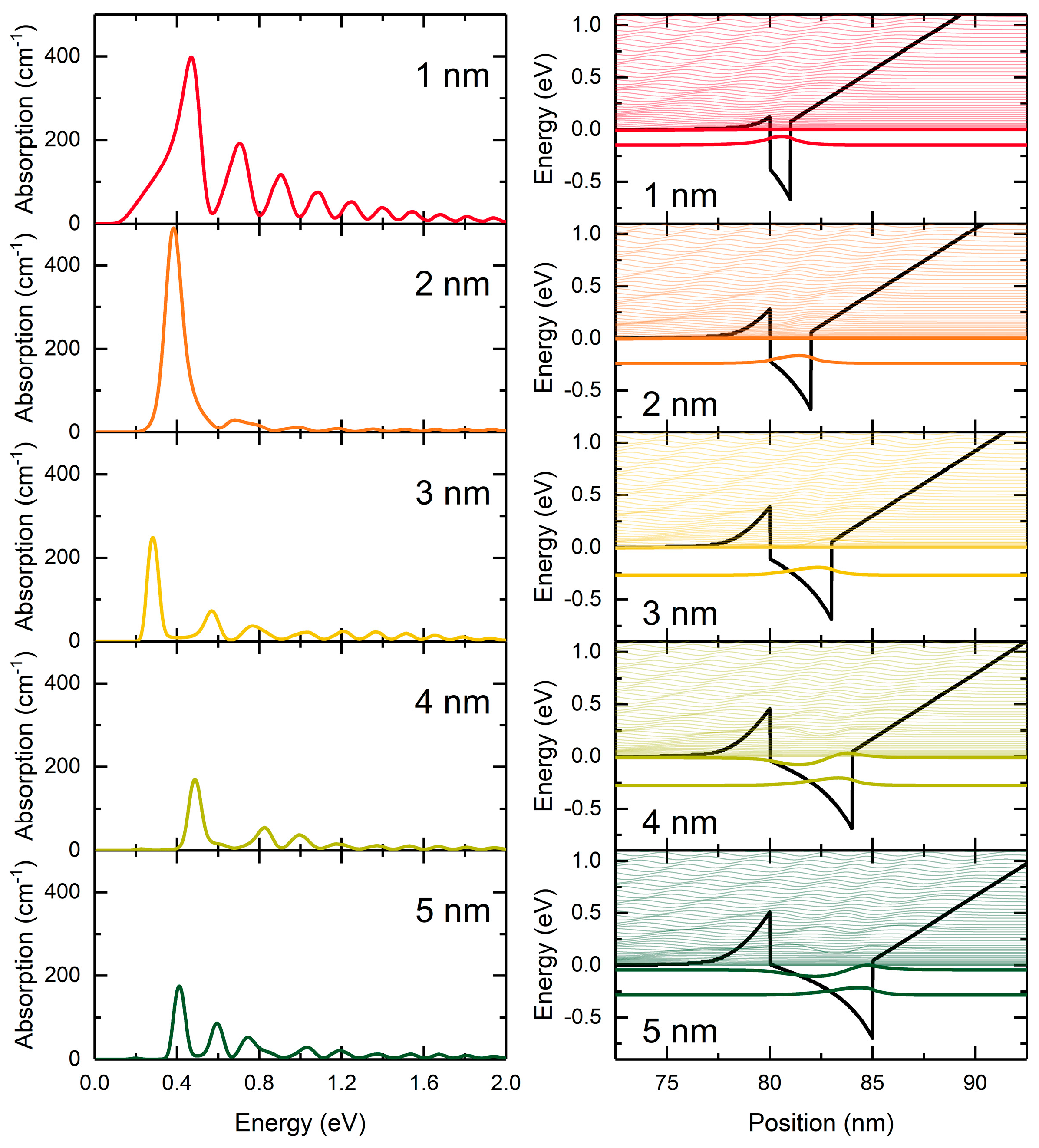
We also checked how the absorption of our diode changed when we increased the well width in Figure 2. In Figure 9, we plot the absorption spectra (at V = 0) for single wells of increasing widths, together with the corresponding potential profiles. The highest absorption peak is observed for a well width of 2 nm, although the oscillations diminish rapidly. This behavior of the absorption coefficient stems from the calculated matrix element. The results indicate that the peak positions and widths primarily reflect the energy dependence of the matrix element. For wider wells, the intensity of the lines decreases. The left-hand barrier (colored with grey in Figure 2) increases with the increasing well width. Above the 4 nm well thickness, the second bound state appears in the well. This leads to the nonmonotonic dependence of the first peaks in the sequence (both in terms of intensity and position). Notably, the strongest absorption lines are observed for well widths of up to 3 nm.
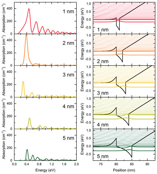
Figure 9.
Absorption spectra for the diode from Figure 2 (at V = 0) for different widths of the In0.2Ga0.8N well and corresponding band profiles and wavefunctions.
4. Summary and Conclusions
We propose an InGaN/AlGaN diode structure which should enable the observation of oscillations in absorption from the ground state to the continuum. This is a better system for observing absorption oscillations than a single quantum well in an external electric field. Our calculation employs a semi-classical drift-diffusion/Poisson–Schrodinger solver for determining the band structure.
The case of InGaN/AlGaN quantum wells differs from the previously studied GaAs/AlGaAs structures due to higher effective mass and high built-in fields. However, the absorption from the ground state in a narrow well to the continuum above reveals similar oscillations as in GaAs wells. Resonances result from the interference of wavefunctions reflected from the edges of the well and from the right-hand side potential barrier. The absorption oscillations are the most pronounced for well widths below 3 nm, for which there is exactly one bound state. The amplitude and period of the oscillations can be tuned by an external voltage. The amplitude is greatest while the period is smallest for positive voltages of 2 V, that is, below the turn-on voltage of the n-i-p diode. Oscillations do not depend on temperature, as they mainly follow the maxima of the matrix element of momentum.
Supplementary Materials
The following supporting information can be downloaded at: https://www.mdpi.com/article/10.3390/nano15030174/s1, Table S1: Material database used in one dimensional Poisson-Schrodinger solver developed by Wu [17,18] based on Refs. [19,20,21].
Author Contributions
Conceptualization, W.T., M.G.-K. and M.Ż.; methodology, M.G.-K. and W.T.; software, M.G.-K. and M.Ż.; validation, W.T.; investigation, M.G.-K. and M.Ż.; writing—original draft preparation, W.T. and M.G.-K.; writing—review and editing, M.Ż.; visualization, M.Ż.; supervision, W.T.; All authors have read and agreed to the published version of the manuscript.
Funding
This work was supported by National Science Centre, Poland, grant no. 2023/49/N/ST7/03786.
Data Availability Statement
Dataset available on request from the authors.
Conflicts of Interest
The authors declare no conflicts of interest. The funders had no role in the design of the study; in the collection, analyses, or interpretation of data; in the writing of the manuscript; or in the decision to publish the results.
References
- Liu, H.C.; Capasso, F. Intersubband Transitions in Quantum Wells: Physics and Device Applications I; Semiconductors and Semimetals; Academic Press: San Diego, CA, USA, 2000; Volume 62. [Google Scholar]
- Fafard, S. Energy levels in quantum wells with capping barrier layer of finite size: Bound states and oscillatory behavior of the continuum states. Phys. Rev. B 1992, 46, 4659–4666. [Google Scholar] [CrossRef] [PubMed]
- Fafard, S.; Fortin, E.; Roth, A.P. Effects of an electric field on the continuum energy levels in InGaAs/GaAs quantum wells terminated with thin cap layers. Phys. Rev. B 1993, 47, 8089–10595. [Google Scholar] [CrossRef]
- Colocci, M.; Martinez-Pastor, J.; Gurioli, M. Above-barrier resonant transitions in AlGaAs/A1As/GaAs heterostructures. Phys. Rev. B 1993, 48, 8089–8094. [Google Scholar] [CrossRef] [PubMed]
- Lee, C.D.; Son, J.S.; Leem, J.Y.; Noh, S.K.; Kyu-Seok Lee Lee, C.; Hwang, I.S.; Park, H.Y. Direct observation of above-barrier quasibound states in InGaAs/AlAs/GaAs quantum wells. Phys. Rev. B 1996, 54, 1541–1544. [Google Scholar] [CrossRef] [PubMed]
- Trzeciakowski, W.; Gurioli, M. Electric-field effects in semiconductor quantum wells. Phys. Rev. B 1991, 44, 3880–3890. [Google Scholar] [CrossRef] [PubMed]
- Kuo, D.M.-T.; Chang, Y.-C. Intersubband electroabsorption spectra of semiconductor quantum wells. J. Appl. Phys. 2000, 87, 2936–2940. [Google Scholar] [CrossRef]
- Vorob’ev, L.E.; Zibik, E.A.; Firsov, D.A.; Shalygin, V.A.; Nashchekina, O.N.; Saidashev, I.I. Modulation of optical absorption of GaAs/AlGaAs quantum wells in a transverse electric field. Semiconductors 1998, 32, 754–756. [Google Scholar] [CrossRef]
- Gmachl, C.; Ng, H.M.; Cho, A.Y. Intersubband absorption in GaN/AlGaN multiple quantum wells in the wavelength range of λ∼1.75–4.2 μm. Appl. Phys. Lett. 2000, 77, 334–336. [Google Scholar] [CrossRef]
- Machhadani, H.; Kandaswamy, P.; Sakr, S.; Vardi, A.; Wirtmüller, A.; Nevou, L.; Guillot, F.; Pozzovivo, G.; Tchernycheva, M.; Lupu, A.; et al. GaN/AlGaN intersubband optoelectronic devices. New J. Phys. 2009, 11, 125023. [Google Scholar] [CrossRef]
- Hofstetter, D.; Baumann, E.; Giorgetta, F.R.; Théron, R.; Wu, H.; Schaff, W.J.; Dawlaty, J.; George, P.A.; Eastman, L.F.; Rana, F.; et al. Intersubband transition-based processes and devices in AlN/GaN-based heterostructures. Proc. IEEE 2010, 98, 1234–1248. [Google Scholar] [CrossRef]
- Beeler, M.; Trichas, E.; Monroy, E. III-nitride semiconductors for intersubband optoelectronics: A review. Semicond. Sci. Technol. 2013, 28, 074022. [Google Scholar] [CrossRef]
- Gładysiewicz, M.; Kudrawiec, R. Random approach to determine the broadening of intersubband and interband transitions in (In)GaN/Al(In)N quantum wells. J. Phys. Condens. Matter 2010, 22, 485801. [Google Scholar] [CrossRef]
- Yıldırım, H.; Aslan, B. Intersubband transitions in InGaN/InGaN/GaN staggered quantum wells. J. Appl. Phys. 2014, 115, 164306. [Google Scholar] [CrossRef]
- Chen, G.; Wang, X.Q.; Rong, X.; Wang, P.; Xu, F.J.; Tang, N.; Qin, Z.X.; Chen, Y.H.; Shen, B. Intersubband Transition in GaN/InGaN Multiple Quantum Wells. Sci. Rep. 2015, 5, 11485. [Google Scholar] [CrossRef]
- Monavarian, M.; Xu, J.; Fireman, M.N.; Nookala, N.; Wu, F.; Bonef, B.; Qwah, K.S.; Young, E.C.; Belkin, M.A.; Speck, J.S. Structural and optical properties of nonpolar m- and a-plane GaN/AlGaN heterostructures for narrow-linewidth mid-infrared intersubband transitions. Appl. Phys. Lett. 2020, 116, 201103. [Google Scholar] [CrossRef]
- Wu, Y.-R.; Chiu, C.; Chang, C.-Y.; Yu, P.; Kuo, H.-C. Size-Dependent Strain Relaxation and Optical Characteristics of InGaN/GaN Nanorod LEDs. IEEE J. Sel. Top. Quantum Electron. 2009, 15, 1226–1233. [Google Scholar] [CrossRef]
- Wu, Y.-R.; Shivaraman, R.; Wang, K.-C.; Speck, J.S. Analyzing the physical properties of InGaN multiple quantum well light emitting diodes from nano scale structure. Appl. Phys. Lett. 2012, 101, 083505. [Google Scholar] [CrossRef]
- Ambacher, O.; Majewski, J.; Miskys, C.; Link, A.; Hermann, M.; Eickhoff, M.; Stutzmann, M.; Bernardini, F.; Fiorentini, V.; Tilak, V.; et al. Pyroelectric properties of Al(In)GaN/GaN hetero- and quantum well structures. J. Phys. Condens. Matter 2002, 14, 3399. [Google Scholar] [CrossRef]
- Vurgaftman, I.; Meyer, J.R. Band parameters for nitrogen-containing semiconductors. J. Appl. Phys. 2003, 94, 3675–3696. [Google Scholar] [CrossRef]
- Chuang, S.L.; Chang, C.S. k·p method for strained wurtzite semiconductors. Phys. Rev. B 1996, 54, 2491. [Google Scholar] [CrossRef] [PubMed]
- BenDaniel, D.J.; Duke, C.B. Space-Charge Effects on Electron Tunneling. Phys. Rev. B 1966, 152, 683–692. [Google Scholar] [CrossRef]
- Salejda, W.; Tyc, M.; Andrzejewski, J.; Kubisa, M.; Misiewicz, J.; Just, M.; Ryczko, K. New Numerical Matrix Methods of Solving the Quasi-One-Dimensional Effective-Mass Equation. Acta Phys. Pol. A 1999, 95, 881–896. [Google Scholar] [CrossRef]
- Gładysiewicz, M.; Kudrawiec, R.; Muzioł, G.; Turski, H.; Skierbiszewski, C. Theoretical and Experimental Studies on Material Gain for Wide Polar InGaN Quantum Well-Mechanism Leading to Electric Field Screening and Lasing. Adv. Phys. Res. 2023, 2, 2200107. [Google Scholar] [CrossRef]
- Gladysiewicz, M.; Skierbiszewski, C.; Kudrawiec, R. Material Gain in Polar GaInN and AlGaN Quantum Wells: How to Overcome the ‘Dead’ Width for Light Emitters in These QW Systems? IEEE J. Sel. Top. Quantum Electron. 2022, 28, 1501509. [Google Scholar] [CrossRef]
- Jarema, M.; Gladysiewicz, M.; Janicki, L.; Zdanowicz, E.; Turski, H.; Muziol, G.; Skierbiszewski, C.; Kudrawiec, R. Inhomogeneous broadening of optical transitions observed in photoluminescence and modulated reflectance of polar and non-polar InGaN quantum wells. J. Appl. Phys. 2020, 127, 035702. [Google Scholar] [CrossRef]
- Baranowski, M.; Janicki, L.; Gladysiewicz, M.; Welna, M.; Latkowska, M.; Misiewicz, J.; Marona, L.; Schiavon, D.; Perlin, P.; Kudrawiec, R. Direct evidence of photoluminescence broadening enhancement by local electric field fluctuations in polar InGaN/GaN quantum wells. Jpn. J. Appl. Phys. 2018, 57, 9. [Google Scholar]
- Jarema, M.; Gladysiewicz, M.; Zdanowicz, E.A.; Bellet-Amalric, E.; Monroy, E.; Kudrawiec, R. On intrinsic Stokes shift in wide GaN/AlGaN polar quantum wells. Semicond. Sci. Technol. 2019, 34, 075021. [Google Scholar] [CrossRef]
- Chow, W.; Kira, M.; Koch, S.W. Microscopic theory of optical nonlinearities and spontaneous emission lifetime in group-III nitride quantum wells. Phys. Rev. B 1999, 60, 1947–1952. [Google Scholar] [CrossRef]
- Bin-He, W. Transient Intersubband Optical Absorption in Double Quantum Well Structure. Commun. Theor. Phys. 2005, 43, 759–764. [Google Scholar] [CrossRef]
- Ndebeka-Bandou, C.; Carosella, F.; Ferreira, R.; Wacker, A.; Bastard, G. Free carrier absorption and inter-subband transitions in imperfect heterostructures. Semicond. Sci. Technol. 2014, 29, 023001. [Google Scholar] [CrossRef]
- Smith, R.P.; Funk, A.C.; Mirin, R.P.; Cundiff, S.T.; Steiner, J.T.; Schafer, M.; Kira, M.; Koch, S.W. Extraction of Many-Body Configurations from Nonlinear Absorption in Semiconductor Quantum Wells. Phys. Rev. Lett. 2010, 104, 247401. [Google Scholar] [CrossRef] [PubMed]
- Sfuncia, G.; Nicotra, G.; Giannazzo, F.; Pécz, B.; Gueorguiev, G.K.; Kakanakova-Georgieva, A. 2D graphitic-like gallium nitride and other structural selectivity in confinement at the graphene/SiC interface. CrystEngComm 2023, 25, 5810. [Google Scholar] [CrossRef]
- Filho, M.A.M.; Hsiao, C.-L.; dos Santos, R.B.; Hultman, L.; Birch, J.; Gueorguiev, G.K. Self-Induced Core–Shell InAlN Nanorods: Formation and Stability Unraveled by Ab Initio Simulations. ACS Nanosci. Au 2023, 3, 84–93. [Google Scholar] [CrossRef]
- Scheibenzuber, W.G.; Schwarz, U.T.; Sulmoni, L.; Carlin, J.-F.; Castiglia, A.; Grandjean, N. Bias-dependent absorption coefficient of the absorber section in GaN-based multisection laser diodes. Appl. Phys. Lett. 2010, 97, 181103. [Google Scholar] [CrossRef]
- Yang, Z.-H.; Ullrich, C.A. Direct calculation of exciton binding energies with time-dependent density-functional theory. Phys. Rev. B 2013, 87, 195204. [Google Scholar] [CrossRef]
- Baeten, M.; Wouters, M. Many-body effects of a two-dimensional electron gas on trion-polaritons. Phys. Rev. B 2015, 91, 115313. [Google Scholar] [CrossRef]
- Hwang, E.H.; Throckmorton, R.E.; Sarma, S.D. Plasmon-pole approximation for many-body effects in extrinsic graphene. Phys. Rev. B 2018, 98, 195140. [Google Scholar] [CrossRef]


Disclaimer/Publisher’s Note: The statements, opinions and data contained in all publications are solely those of the individual author(s) and contributor(s) and not of MDPI and/or the editor(s). MDPI and/or the editor(s) disclaim responsibility for any injury to people or property resulting from any ideas, methods, instructions or products referred to in the content. |
© 2025 by the authors. Licensee MDPI, Basel, Switzerland. This article is an open access article distributed under the terms and conditions of the Creative Commons Attribution (CC BY) license (https://creativecommons.org/licenses/by/4.0/).