
Structural and Transport Properties of Thin InAs Layers Grown on InxAl1−xAs Metamorphic Buffers

 , ,
, ,  and
and
Abstract
1. Introduction
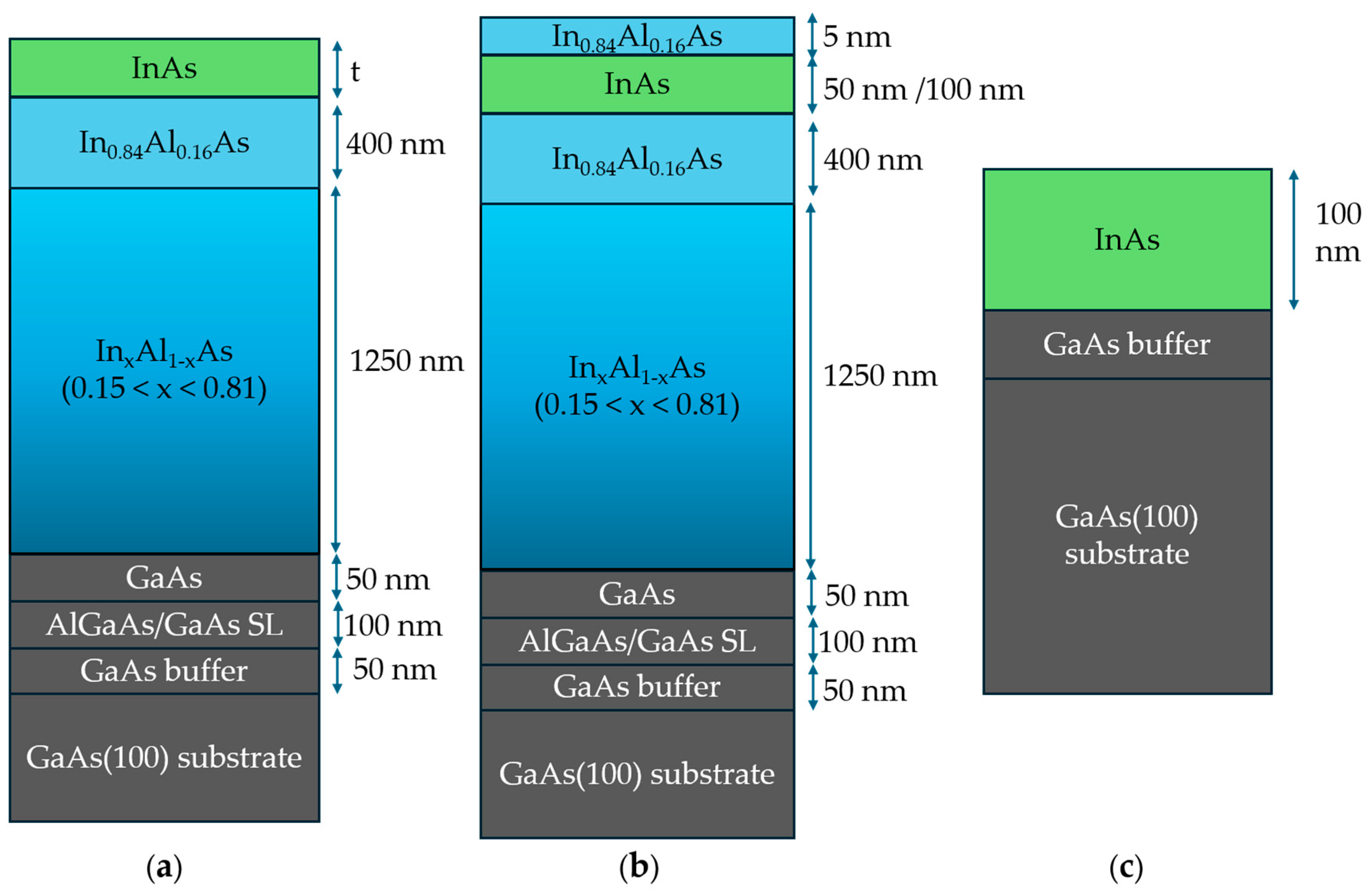
2. Materials and Methods
3. Results and Discussion
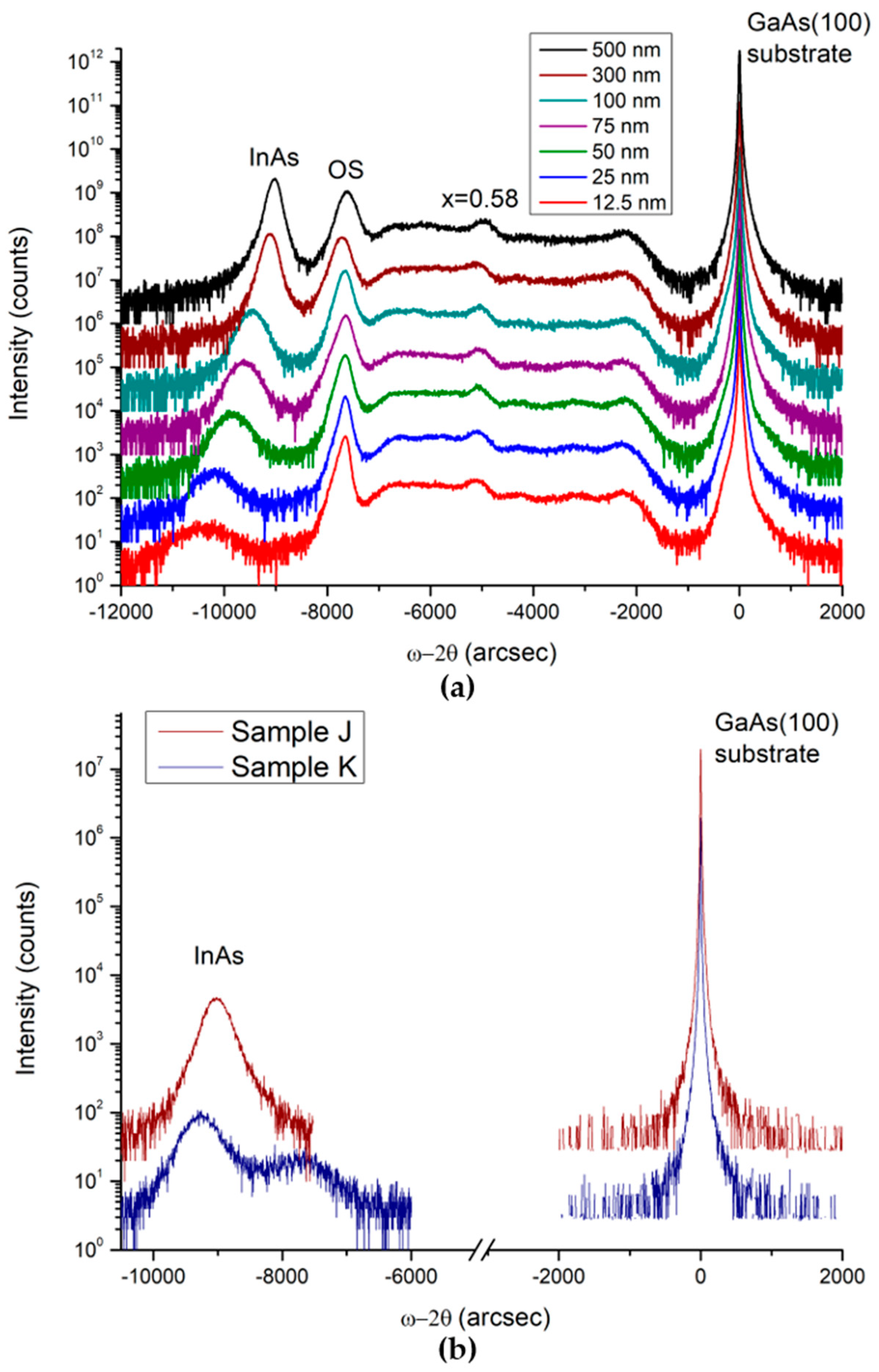
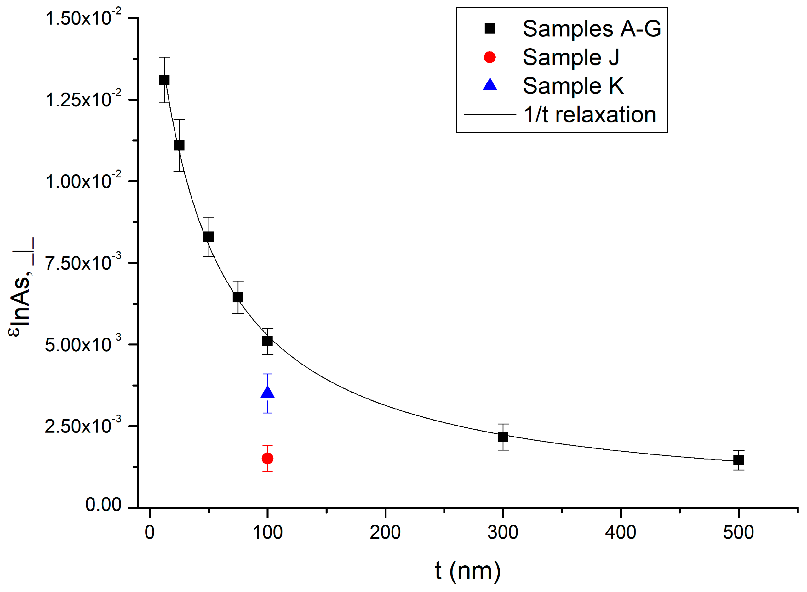
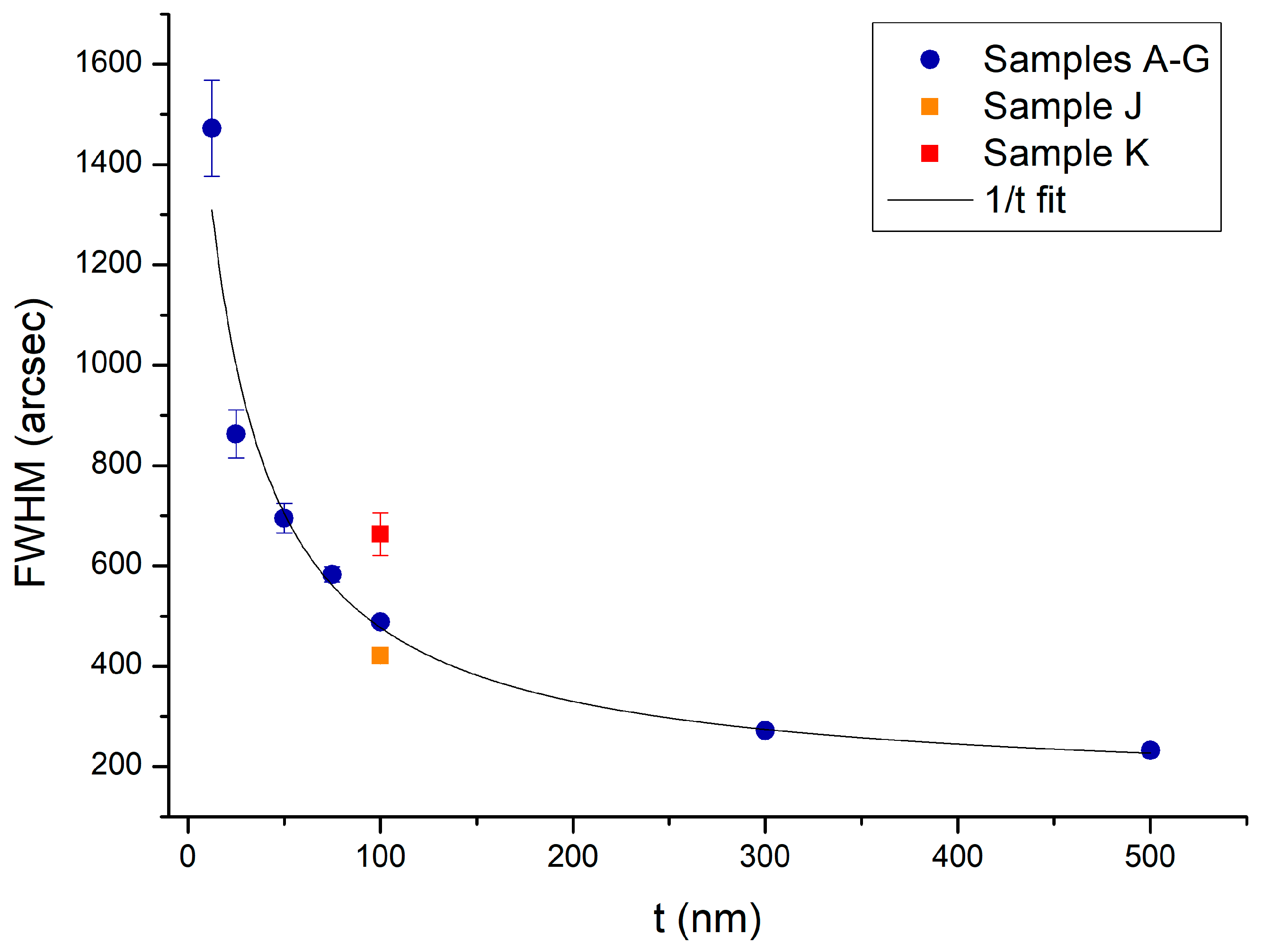
3.1. Structural Properties
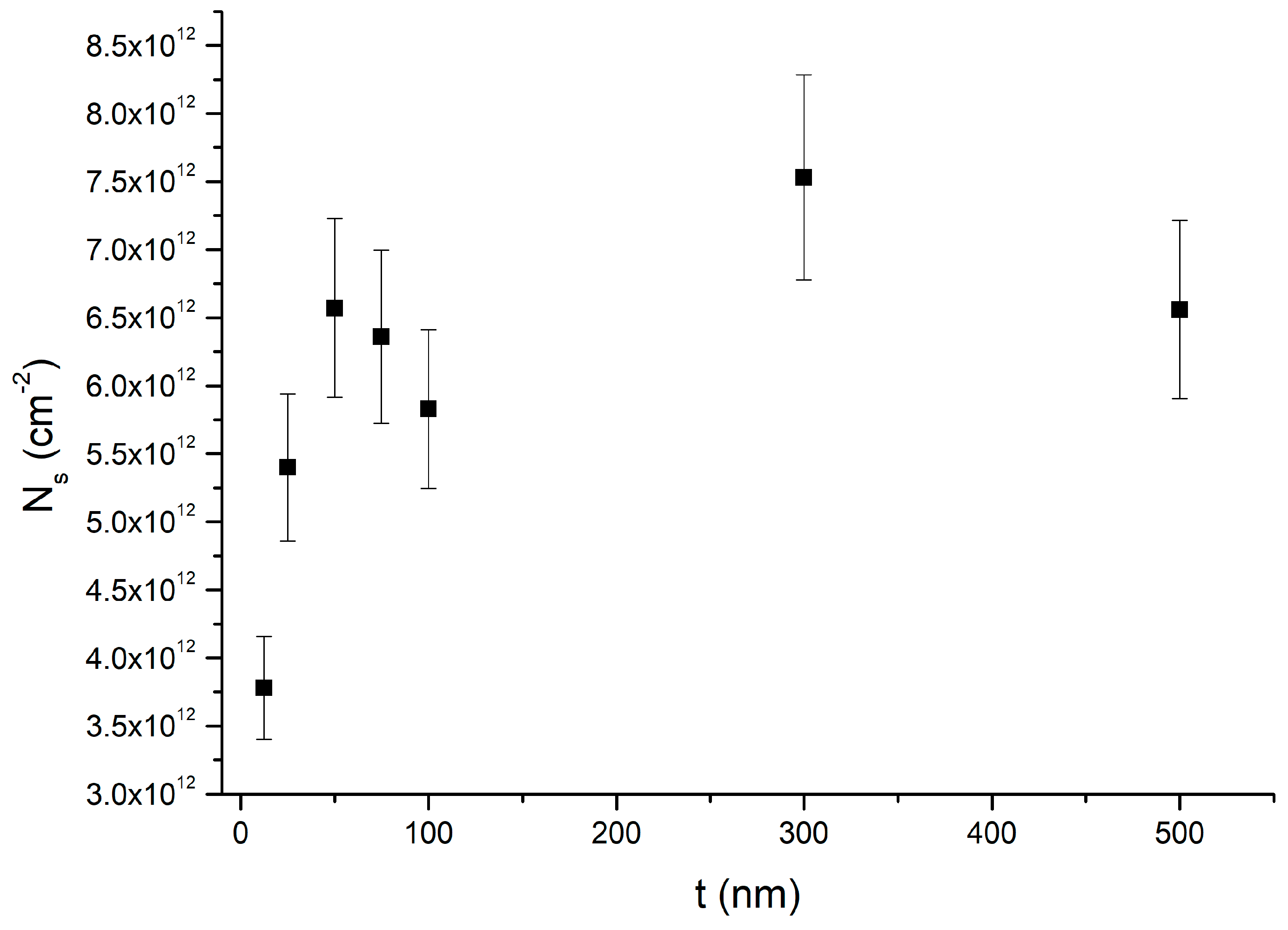
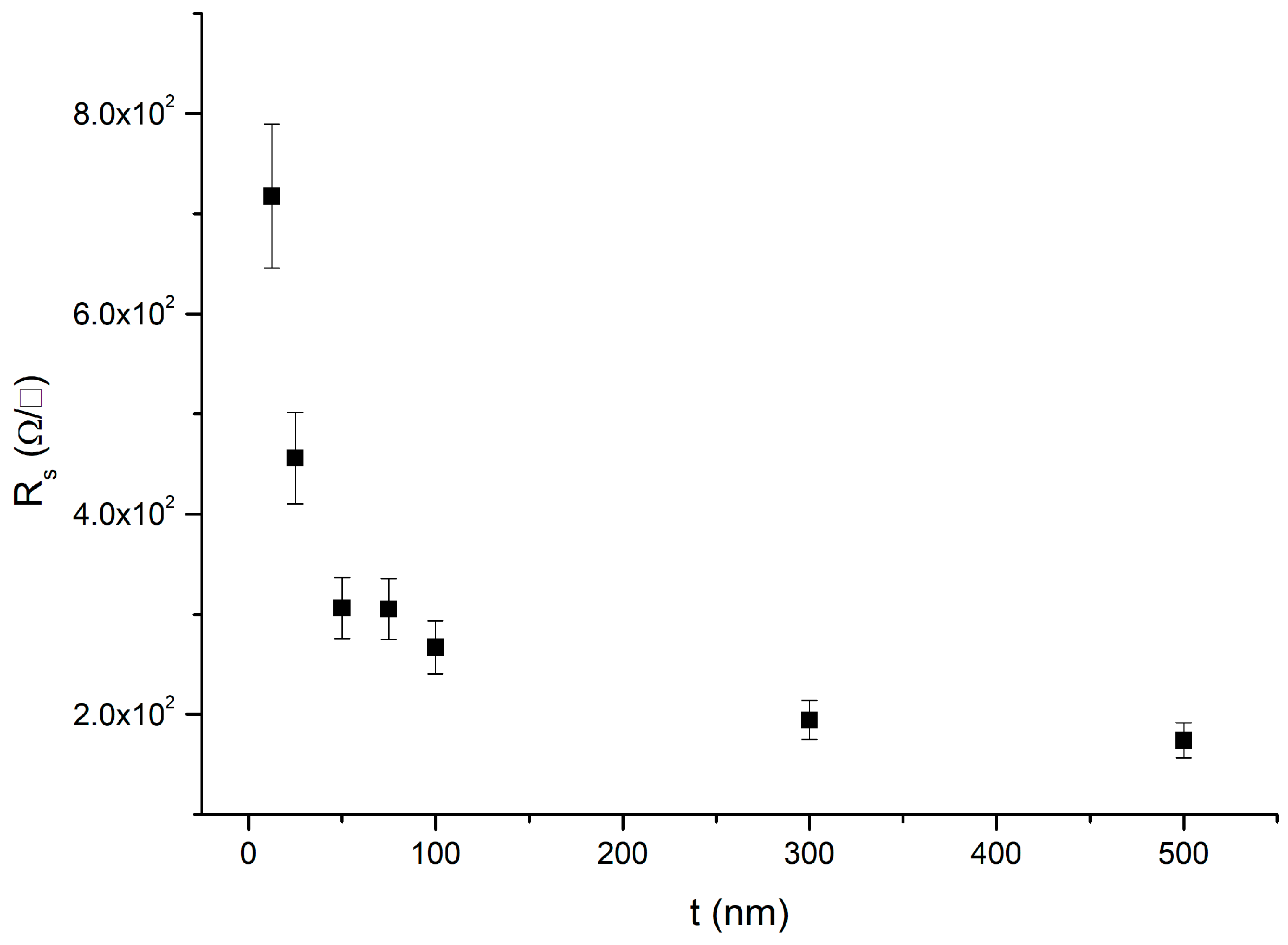
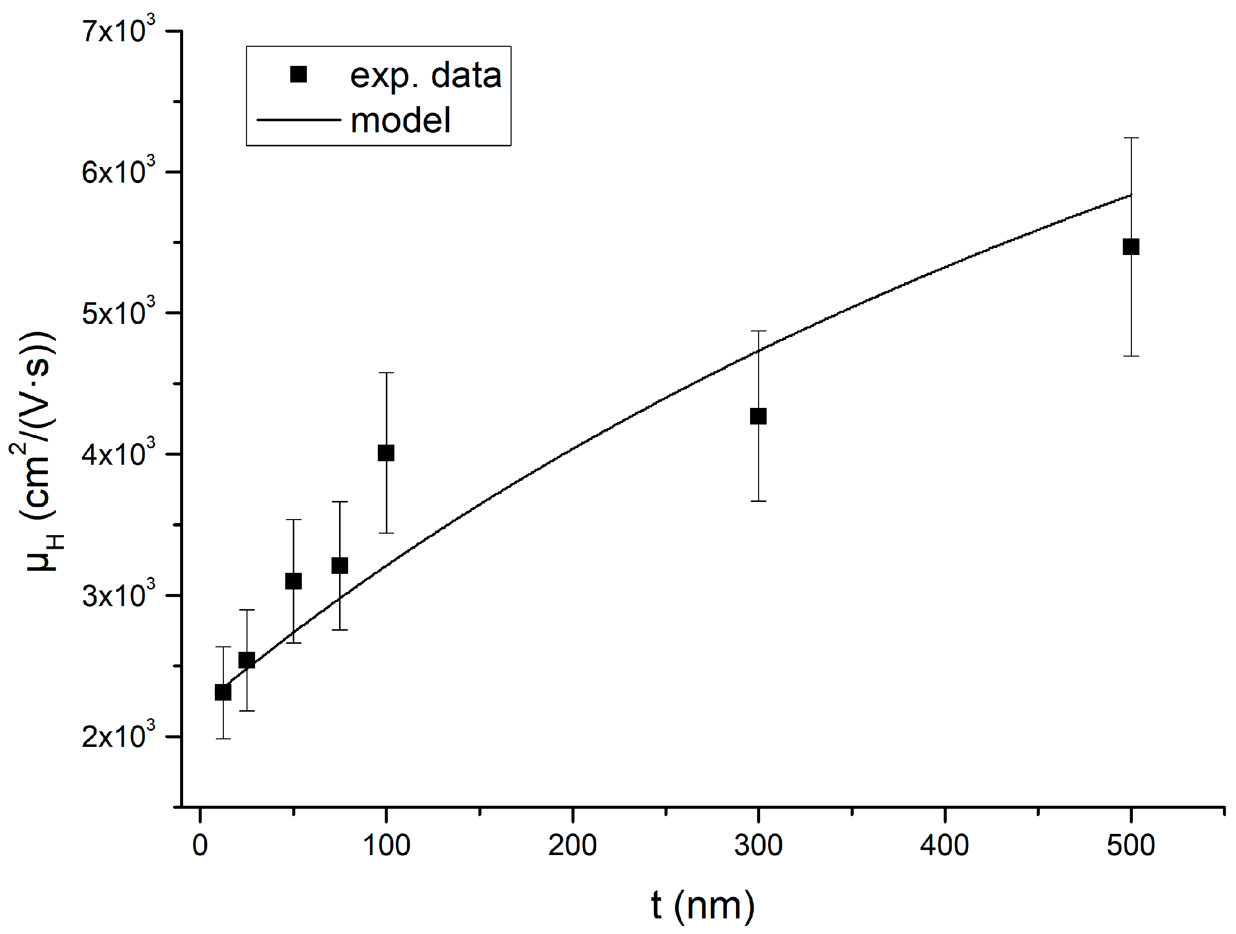
3.2. Transport Properties
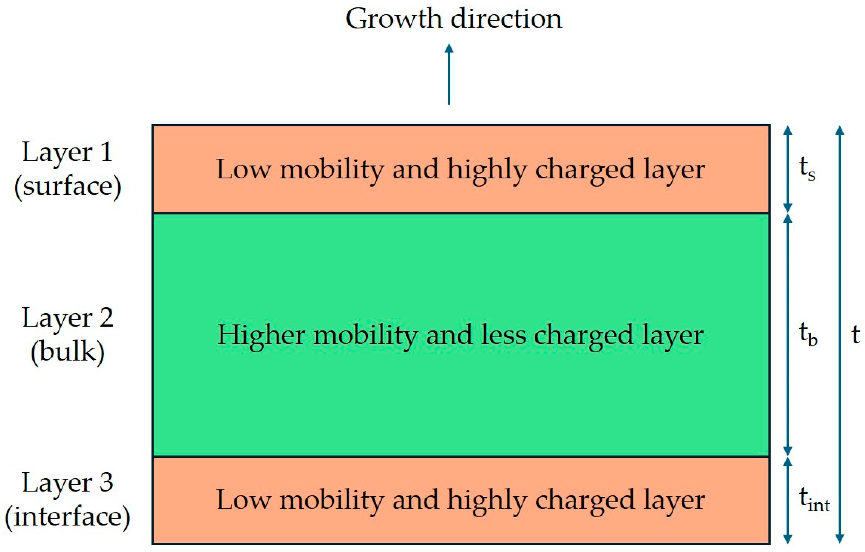
- Layer 1 (surface layer): since the InAs surface Fermi level is pinned in the conduction band, which is bent at the InAs–vacuum interface, surface charge accumulation takes place, and the presence of a low-mobility surface layer is expected. A reasonable estimation for the thickness of this layer is the Debye length LD. In particular, since the carrier concentration nb of a bulk-like near-intrinsic InAs crystal is of the order of 1 × 1015 cm−3 [27], we expectfor T = 300 K and the relative permittivity of InAs κ = 12.5.
- Layer 2 (bulk layer): the InAs layer corresponding to an InAs bulk crystal.
- Layer 3 (interface layer): a low-mobility and charged interface layer is expected to be present because of the nucleation of misfit dislocations in InAs layers that are thicker than the critical thickness of InAs on In0.84Al0.16As. Wolkenberg et al. [27] estimated the thickness of this highly defected layer for InAs on GaAs to be 1.8 nm. This value corresponds roughly to the critical thickness of InAs on GaAs. Here, we estimate this highly defected layer to be around 10 nm thick, which is the estimated critical thickness of InAs on this metamorphic buffer.
- One highly defected interface layer with thickness tint and carrier concentration nint, which is layer 3 of the three-channel model.
- One layer that stands for the ’bulk–surface’ transport properties with thickness (t − tint) and carrier concentration nbs.
4. Conclusions
Supplementary Materials
Author Contributions
Funding
Data Availability Statement
Acknowledgments
Conflicts of Interest
References
- Paghi, A.; Trupiano, G.; de Simoni, G.; Arif, O.; Sorba, L.; Giazotto, F. InAs on Insulator: A New Platform for Cryogenic Hybrid Superconducting Electronics. Adv. Funct. Mater. 2024, 2416957. [Google Scholar] [CrossRef]
- Godinho, N.; Brunnschweiler, A. Epitaxial indium arsenide by vacuum evaporation. Solid-State Electron. 1970, 13, 47–50. [Google Scholar] [CrossRef]
- Cronin, G.R.; Conrad, R.W.; Borrello, S.R. Epitaxial InAs on Semi-Insulating GaAs Substrate. J. Electrochem. Soc. 1966, 113, 1336–1338. [Google Scholar] [CrossRef]
- McCarthy, J.P. Preparation and properties of epitaxial InAs. Solid-State Electron. 1967, 10, 649–655. [Google Scholar] [CrossRef]
- Yano, M.; Nogami, M.; Matsushima, Y.; Kimata, M. Molecular Beam Epitaxial Growth of InAs. Jpn. J. Appl. Phys. 1977, 16, 2131–2137. [Google Scholar] [CrossRef]
- Meggitt, B.T.; Parker, E.H.C.; King, R.M. Thin InAs epitaxial layers grown on (100) GaAs substrates by molecular beam deposition. Appl. Phys. Lett. 1978, 33, 528–530. [Google Scholar] [CrossRef]
- Kalem, S.; Inn, C.J.; Morkoc, H.; Bean, R.; Zanio, K. Growth and transport properties of InAs epilayers on GaAs. Appl. Phys. Lett. 1988, 53, 1647–1649. [Google Scholar] [CrossRef]
- Wang, P.D.; Holmes, S.N.; Tan, L.; Stradling, R.A.; Ferguson, I.T.; de Oliveira, A.G. Electrical and magneto-optical of MBE InAs on GaAs. Semicond. Sci. Technol. 1992, 7, 767. [Google Scholar] [CrossRef]
- Zhou, S.; Wan, Z.; Lei, Y.; Tang, B.; Tao, G.; Du, P.; Zhao, X. InGaN quantum well with gradually varying indium content for high-efficiency GaN-based green light-emitting diodes. Opt. Lett. 2022, 47, 1291–1294. [Google Scholar] [CrossRef] [PubMed]
- Sun, Y.; Cui, G.; Guo, K.; Zhang, J.; Zhuo, N.; Wang, L.; Liu, S.; Jia, Z.; Fei, T.; Li, K.; et al. Quantum cascade lasers grown by MOCVD. J. Semicond. 2023, 44, 121901. [Google Scholar] [CrossRef]
- Park, J.-S.; Tang, M.; Chen, S.; Liu, H. Heteroepitaxial Growth of III-V Semiconductors on Silicon. Crystals 2020, 10, 1163. [Google Scholar] [CrossRef]
- Baliga, B.J.; Ghandhi, S.K. Heteroepitaxial InAs Grown on GaAs from Triethylindium and Arsine: I. Growth Characterization. J. Electrochem. Soc. 1974, 121, 1642. [Google Scholar] [CrossRef]
- Watkins, S.P.; Tran, C.A.; Soerensen, G.; Cheung, H.D.; Ares, R.A.; Lacroix, Y.; Thewalt, M.L.W. Characterization of very high purity InAs grown using trimethylindium and tertiarybutylarsine. J. Electron. Mater. 1995, 24, 1583–1590. [Google Scholar] [CrossRef]
- Botha, L.; Shamba, P.; Botha, J.R. Electrical characterization of InAs thin films. Phys. Stat. Sol. (C) 2008, 5, 620–622. [Google Scholar] [CrossRef]
- Pödör, B. Electron mobility in plastically deformed Germanium. Phys. Stat. Sol. (B) 1966, 16, K167–K170. [Google Scholar] [CrossRef]
- Chang, C.-A.; Serrano, C.M.; Chang, L.L.; Esaki, L. Effect of lattice mismatch on the electron mobilities of InAs grown on GaAs by MBE. J. Vac. Sci. Technol. 1980, 17, 603–605. [Google Scholar] [CrossRef]
- Arif, O.; Canal, L.; Ferrari, E.; Ferrari, C.; Lazzarini, L.; Nasi, L.; Paghi, A.; Heun, S.; Sorba, L. Influence of an Overshoot Layer on the Morphological, Structural, Strain, and Transport Properties of InAs Quantum Wells. Nanomaterials 2024, 14, 592. [Google Scholar] [CrossRef] [PubMed]
- Haga, T.; Kataoka, M.; Matsumura, N.; Muto, S.; Nakata, Y.; Yokoyama, N. Interdiffusion between InAs Quantum Dots and GaAs Matrices. Jpn. J. Appl. Phys. 1997, 36, L1113–L1115. [Google Scholar] [CrossRef]
- Nabetani, Y.; Ishikawa, T.; Noda, S.; Sasaki, A. Initial growth stage and optical properties of a three-dimensional InAs structure on GaAs. J. Appl. Phys. 1994, 76, 347–351. [Google Scholar] [CrossRef]
- NSM Archive—Physical Properties of Semiconductors. Available online: https://www.ioffe.ru/SVA/NSM/Semicond/InAs/mechanic.html (accessed on 12 November 2024).
- Benali, A.; Rajak, P.; Ciancio, R.; Plaisier, J.R.; Heun, S.; Biasiol, G. Metamorphic InAs/InGaAs QWs with electron mobilities exceeding 7 × 105 cm2/Vs. J. Cryst. Growth 2022, 593, 126768. [Google Scholar] [CrossRef]
- Dunstan, D.J.; Young, S.; Dixon, R.H. Geometrical theory of critical thickness and relaxation in strained-layer growth. J. Appl. Phys. 1991, 70, 3038–3045. [Google Scholar] [CrossRef]
- Ayers, J.E. The measurement of threading dislocation densities in semiconductor crystals by X-ray diffraction. J. Cryst. Growth 1994, 135, 71–77. [Google Scholar] [CrossRef]
- Scherrer, P. Nachrichten von der Gesellschaft der Wissenschaften zu Göttingen. Math.-Phys. Kl. 1918, 2, 98–100. Available online: https://www.digizeitschriften.de/id/252457811_1918?tify=%7B%22pages%22%3A%5B102%5D%2C%22view%22%3A%22toc%22%7D (accessed on 19 January 2025).
- Gopal, V.; Souw, V.; Chen, E.-H.; Kvam, E.P.; McElfresh, M.; Woodall, J.M. Temperature-dependent transport properties of InAs films grown on lattice-mismatched GaP. J. Appl. Phys. 2000, 87, 1350–1355. [Google Scholar] [CrossRef]
- Okamoto, A.; Geka, H.; Shibasaki, I.; Yoshida, K. Transport properties of InSb and InAs thin films on GaAs substrates. J. Cryst. Growth 2005, 278, 604–609. [Google Scholar] [CrossRef]
- Wolkenberg, A.; Przesławski, T.; Kaniewski, J.; Bąk-Misiuk, J.; Regiński, K. Thickness dependence of the structural and electrical properties of InAs layers epitaxially grown by MBE on GaAs (001). Mater. Sci. Eng. B 2000, 77, 250–254. [Google Scholar] [CrossRef]
- Petritz, R.L. Theory of an experiment for measuring the mobility and density of carriers in the space-charge region of a semiconductor surface. Phys. Rev. 1958, 110, 1254. [Google Scholar] [CrossRef]
- Nedoluha, A.; Koch, K.M. Zum Mechanismus der Widerstandsänderung im Magnetfeld. Z. Phys. 1952, 132, 608–620. [Google Scholar] [CrossRef]
- Wieder, H.H. Transport coefficients of InAs epilayers. Appl. Phys. Lett. 1974, 25, 206–208. [Google Scholar] [CrossRef]


| Sample | t (nm) | εOS,⊥ (×10−3) | εInAs,⊥ (×10−3) | Rel. (%) |
|---|---|---|---|---|
| A | 12.5 | 0.8 ± 0.2 | 13.1 ± 1.4 | ~0 |
| B | 25 | 0.8 ± 0.2 | 11.1 ± 1.6 | 3 |
| C | 50 | 0.9 ± 0.2 | 8.3 ± 1.2 | 27 |
| D | 75 | 0.8 ± 0.2 | 6.5 ± 0.5 | 43 |
| E | 100 | 0.9 ± 0.2 | 5.1 ± 0.4 | 55 |
| F | 300 | 1.3 ± 0.2 | 2.2 ± 0.3 | 81 |
| G | 500 | 0.5 ± 0.2 | 1.5 ± 0.3 | 90 |
| H | 50 | 0.9 ± 0.2 | 8.5 ± 0.9 | 25 |
| I | 100 | 0.8 ± 0.2 | 5.0 ± 0.4 | 56 |
| J | 100 | no OS | 1.5 ± 0.4 | 98 |
| K | 100 | no OS | 3.5 ± 0.6 | 95 |
| Sample | t (nm) | Ns (×1012 cm−2) | n (×1017 cm−3) |
|---|---|---|---|
| H | 50 | 3.8 ± 0.4 | 7.6 ± 0.8 |
| I | 100 | 4.2 ± 0.4 | 4.2 ± 0.4 |
| J | 100 | 6.8 ± 0.7 | 6.8 ± 0.7 |
| K | 100 | 9.1 ± 0.9 | 9.1 ± 0.9 |
| Sample | t (nm) | Rs (Ω/□) | µH (×103 cm2/(V·s)) |
|---|---|---|---|
| H | 50 | 400 ± 40 | 4.1 ± 0.6 |
| I | 100 | 312 ± 31 | 4.8 ± 0.7 |
| J | 100 | 399 ± 40 | 2.3 ± 0.3 |
| K | 100 | 330 ± 33 | 2.1 ± 0.3 |
Disclaimer/Publisher’s Note: The statements, opinions and data contained in all publications are solely those of the individual author(s) and contributor(s) and not of MDPI and/or the editor(s). MDPI and/or the editor(s) disclaim responsibility for any injury to people or property resulting from any ideas, methods, instructions or products referred to in the content. |
© 2025 by the authors. Licensee MDPI, Basel, Switzerland. This article is an open access article distributed under the terms and conditions of the Creative Commons Attribution (CC BY) license (https://creativecommons.org/licenses/by/4.0/).
Share and Cite
Senesi, G.; Skibinska, K.; Paghi, A.; Shukla, G.; Giazotto, F.; Beltram, F.; Heun, S.; Sorba, L. Structural and Transport Properties of Thin InAs Layers Grown on InxAl1−xAs Metamorphic Buffers. Nanomaterials 2025, 15, 173. https://doi.org/10.3390/nano15030173
Senesi G, Skibinska K, Paghi A, Shukla G, Giazotto F, Beltram F, Heun S, Sorba L. Structural and Transport Properties of Thin InAs Layers Grown on InxAl1−xAs Metamorphic Buffers. Nanomaterials. 2025; 15(3):173. https://doi.org/10.3390/nano15030173
Chicago/Turabian StyleSenesi, Giulio, Katarzyna Skibinska, Alessandro Paghi, Gaurav Shukla, Francesco Giazotto, Fabio Beltram, Stefan Heun, and Lucia Sorba. 2025. "Structural and Transport Properties of Thin InAs Layers Grown on InxAl1−xAs Metamorphic Buffers" Nanomaterials 15, no. 3: 173. https://doi.org/10.3390/nano15030173
APA StyleSenesi, G., Skibinska, K., Paghi, A., Shukla, G., Giazotto, F., Beltram, F., Heun, S., & Sorba, L. (2025). Structural and Transport Properties of Thin InAs Layers Grown on InxAl1−xAs Metamorphic Buffers. Nanomaterials, 15(3), 173. https://doi.org/10.3390/nano15030173