Article

High-Breakdown and Low-Leakage 4H-SiC MOS Capacitor Based on HfO2/SiO2 Stacked Gate Dielectric in Trench Structures

1
Institute of Wide Bandgap Semiconductors and Future Lighting, Academy for Engineering & Technology, Fudan University, Shanghai 200433, China
2
Shanghai Research Center for Silicon Carbide Power Devices Engineering & Technology, Fudan University, Shanghai 200433, China
3
Institute of Wide Bandgap Semiconductor Materials and Devices, Research Institute of Fudan University in Ningbo, Ningbo 315327, China
*
Author to whom correspondence should be addressed.
Nanomaterials 2025, 15(5), 343; https://doi.org/10.3390/nano15050343
Submission received: 16 January 2025 / Revised: 18 February 2025 / Accepted: 21 February 2025 / Published: 22 February 2025

Abstract

:
The progression of SiC MOSFET technology from planar to trench structures requires optimized gate oxide layers within the trench to enhance device performance. In this study, we investigated the interface characteristics of HfO2 and SiO2/HfO2 gate dielectrics grown by atomic layer deposition (ALD) on SiC trench structures. The trench structure morphology was revealed using scanning electron microscopy (SEM). Atomic force microscopy (AFM) measurements showed that the roughness of both films was below 1nm. Spectroscopic ellipsometry (SE) indicated that the physical thicknesses of HfO2 and SiO2/HfO2 were 38.275 nm and 40.51 nm, respectively, demonstrating their comparable thicknesses. X-ray photoelectron spectroscopy (XPS) analysis of the gate dielectrics revealed almost identical Hf 4f core levels for both HfO2 and the SiO2/HfO2 composite dielectrics, suggesting that the SiO2 interlayer and the SiC substrate had minimal impact on the electronic structure of the HfO2 film. The breakdown electric field of the HfO2 film was recorded as 4.1 MV/cm, with a leakage current at breakdown of 1.1 × 10⁻³A/cm2. The SiO2/HfO2 stacked film exhibited significantly better performance, with a breakdown electric field of 6.5 MV/cm and a marked reduction in leakage current to 3.7 × 10⁻⁴ A/cm2. A detailed extraction and analysis of the leakage current mechanisms were proposed, and the data suggested that the introduction of thin SiO2 interfacial layers effectively mitigated small bandgap offset issues, significantly reducing leakage current and improving device performance.

1. Introduction

SiC MOSFETs offer significant advantages over traditional silicon materials owing to their excellent performance in terms of high-temperature, high-frequency, and high breakdown voltage, wider bandgap, better thermal conductivity, and stronger radiation resistance [1]. These properties make SiC MOSFETs suitable for use in various application fields, including power electronics, electric vehicles, and renewable energy conversion systems. However, transitioning from planar to trench structures in SiC MOSFETs significantly enhances current-carrying capability, reduces on-resistance, increases switching speed, and enables higher rated voltages [2,3]. However, the introduction of trench structures is still challenging for the gate oxide layers [4,5], due to the much higher critical breakdown field strength of SiC than that of traditional materials, as well as the high electric field concentration at the gate corners in trench structures resulting in severe stress on the gate oxide layer [6,7]. Therefore, optimizing the gate oxide layer and solving interface engineering issues have become key research priorities in materials science and engineering. For instance, Wirths et al. [8,9] fabricated planar SiC MOSFETs by incorporating high dielectric constant (high-k) gate dielectrics as a replacement for conventional SiO2 and the yield significantly improved device performance in terms of reduced interface trap density, enhanced threshold voltage stability, and improved device reliability [10,11,12]. Consequently, high-k materials offer a promising approach to enhancing gate oxide performance.
HfO2 with a high dielectric constant (k = 20) and wide bandgap (5.8 eV) is a promising gate dielectric material [13]. However, employing HfO2 as the gate dielectric in 4H-SiC-based MOS devices may lead to high leakage currents due to the low conduction band offset between HfO2 and 4H-SiC [14], which prevents the dielectric from effectively blocking leakage current [15]. Wang et al. conducted first-principles calculations and suggested that introducing a thin SiO2 layer between HfO2 and the SiC substrate could effectively mitigate this issue [16]. Building on this, we implemented this stacked structure in SiC trenches for further investigation. This approach may enhance the band offset, suppress leakage current, and simultaneously preserve the advantages of HfO2’s high dielectric constant [17]. On the other hand, traditional thermal oxidation processes induce an abnormally high interface trap density (Dit) at the SiC/SiO2 interface, which can severely degrade channel mobility [18,19].
To solve the above-considered issues, atomic layer deposition (ALD) was employed in this work to form uniform and high-quality gate oxide layers [20,21]. This deposition method enables precise control over film thickness, composition, and uniformity while facilitating the atomic-scale regulation of the deposition process. Consequently, ALD serves as a powerful technique for studying the microscopic growth process, growth mechanisms, and defect formation in thin films. The impact of the interface was investigated by fabricating HfO2 and SiO2/HfO2 gate dielectrics in trench capacitors. The depth and width of the trench structure and the growth of the high-k films were viewed by SEM. The growth of high-quality films was further confirmed by AFM, spectroscopic ellipsometry (SE), and X-ray photoelectron spectroscopy (XPS). The film thickness was measured using SE, and the bandgap was calculated. It was found that the addition of the SiO2 layer affected the bandgap. The device breakdown electric field (EBR) and leakage current at the onset of breakdown (ION_EBR) were obtained through current-voltage (I–V) measurements along with fitting analysis of the leakage current mechanisms. Capacitance-voltage (C–V) measurements were performed to obtain C–V hysteresis curves, from which the interface trap density (Dit) and effective oxide charge (Neff) were calculated. Fitting analysis of I–V characteristics revealed the different leakage current mechanisms for the two gate dielectrics. This study found that the SiO2/HfO2 stacked dielectric exhibited higher breakdown voltage and lower leakage current, demonstrating feasibility and potential as a gate dielectric in trench structures.

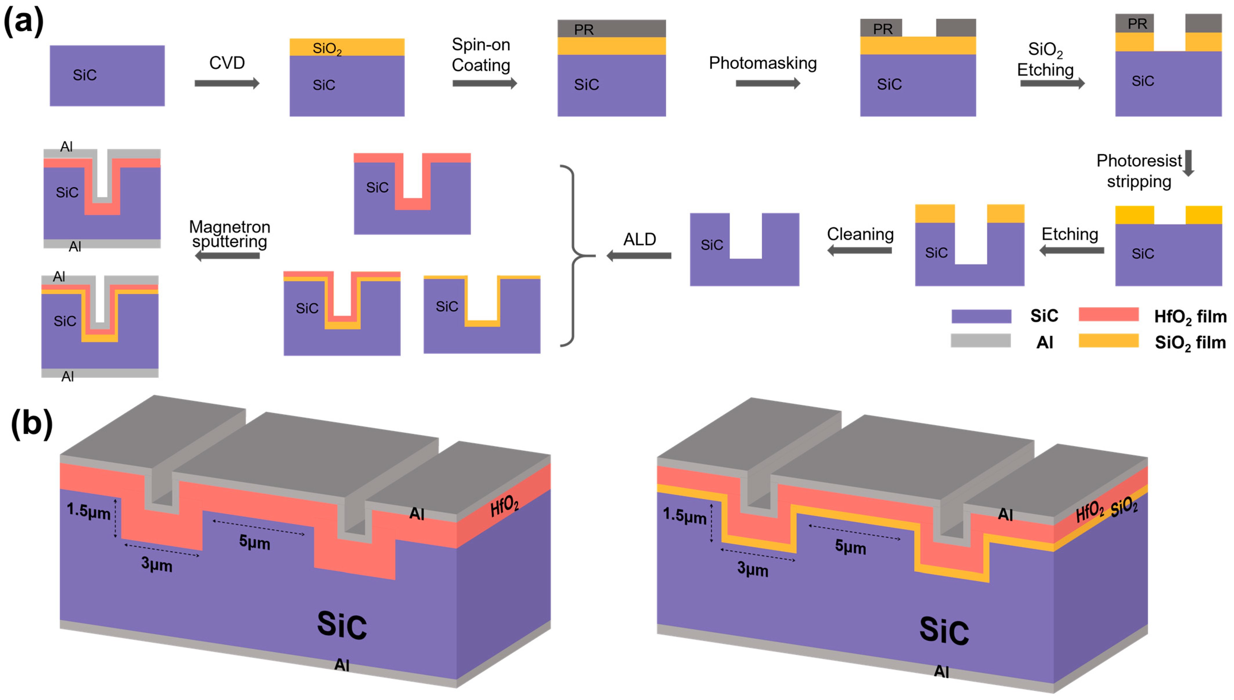
2. Experimental Section

The sample preparation process is shown in Figure 1a. Firstly, a uniform SiO2 film was deposited on the surface of an n-type 4° off-angle silicon face (0001) 4H-SiC epitaxial wafer by chemical vapor deposition (CVD) to form a masking layer. Following the application of a photoresist, photolithography was used to pattern the SiO2 masking layer and define the target trench structure. The photolithography process involved exposure and development processes to create precise patterns on the mask layer, followed by controlling subsequent etching steps to ensure accurate trench dimensions and shapes. The trench structure was aligned along the 1 1 ¯ 00 crystallographic phase of the SiC substrate. After etching the SiO2 masking layer, the photoresist was stripped, and the SiC etching was performed to form the desired trench structure. Next, buffered oxide etch (BOE) technology was used to remove the unprotected areas of the masking layer to form the trench structure. The obtained trench possessed a width of 3 µm, a depth of 1.5 µm, and a spacing of 5 µm, providing a precise structural base for the subsequent thin film deposition. After completion of the trench structure, ALD was employed to uniformly deposit an approximately 40 nm thick gate oxide dielectric layer onto the trench surface. The deposition was performed for 400 cycles at a temperature of 270 °C. TDMAHf and H2O were used as the precursors for Hf and O, respectively, to deposit HfO2 films. In the deposition of SiO2, Bis(diethylamino)silane (BDEAS) was served as the Si precursor, while plasma was used as the O source. The use of ALD technology ensured precise control over the thickness of each layer and guaranteed the formation of a uniform and stable gate oxide layer. Finally, magnetron sputtering was utilized to deposit a 200 nm thick aluminum electrode layer on both the top and bottom sides of the sample. To ensure good electrical performance and stable electrical contact, the front shape of the aluminum electrode was designed as a square with dimensions of 200 µm × 200 µm. The schematic diagrams of the final HfO2 thin film and SiO2/HfO2 bilayer thin film samples are depicted in Figure 1b. This device includes the coexistence of top and trench sidewall dielectric interfaces.
During the manufacturing process, the trench structures at different stages were observed by SEM technique and images of trench structure after etching the SiO2 and SiC layers are presented in Figure 2a,b. The mask layer was then removed by using BOE to yield a satisfactory trench structure with a width of 3 μm, depth of 1.5 μm, and spacing of 5 μm (Figure 2c). As depicted in the SEM image of Figure 2d, the grown gate oxide layer after ALD exhibited excellent consistency even at the trench corners (Figure 2e), highlighting the advantages of ALD when compared to traditional dry oxidation methods in terms of better control over film thickness and uniformity.
The performance of the fabricated devices was evaluated through a series of tests. After the etching process and ALD treatment, the samples were cleaved, and their backsides were attached to a cross-sectional stage. Following a 30 s gold sputtering process, cross-sectional imaging was performed using a Sigma 300 SEM (ZEISS, Oberkochen, Germany) to assess trench etching and film growth. Additional material tests and analyses were then performed on the films after ALD. The film thickness was measured by SE (HORIBA France SAS, Palaiseau, France) equipment. The SiC substrate was parameterized using B-splines, and the thickness and associated optical parameters of the films were determined using the Cauchy dispersion model to characterize the gate dielectric layer. Surface topography analysis was performed using atomic force microscopy (AFM) (Bruker BRK0003, Karlsruhe, Germany) with a scanning range of 25 µm2. The raw data were processed using NanoScopeAnalysis (3.0) (Billerica, MA, USA) software to determine surface roughness. Further analysis of the chemical states of the films was carried out by XPS (Thermo ScientificTM ESCALAB 250Xi, Waltham, MA, USA) spectrometry. To ensure accurate data, a 10 nm etching was performed on the surfaces of both films. All spectral peaks were calibrated using a C 1s peak with a binding energy of 284.8 eV.
The fabricated devices were tested by a TS2000-HP probe station (Hsinchu, Taiwan) and a Keithley 4200A-S (Solon, OH, USA) semiconductor analyzer. The I–V curves were obtained through a gradual increase in gate voltage until reaching dielectric breakdown. The EBR and ION_EBR of MOS samples were determined from the I–V curves. The C–V curves at different frequencies were obtained by scanning the gate voltage at an AC voltage of 30mV. Dit and Neff values of the MOS capacitors’ oxide layer were calculated from the C–V data and all tests were conducted at room temperature.

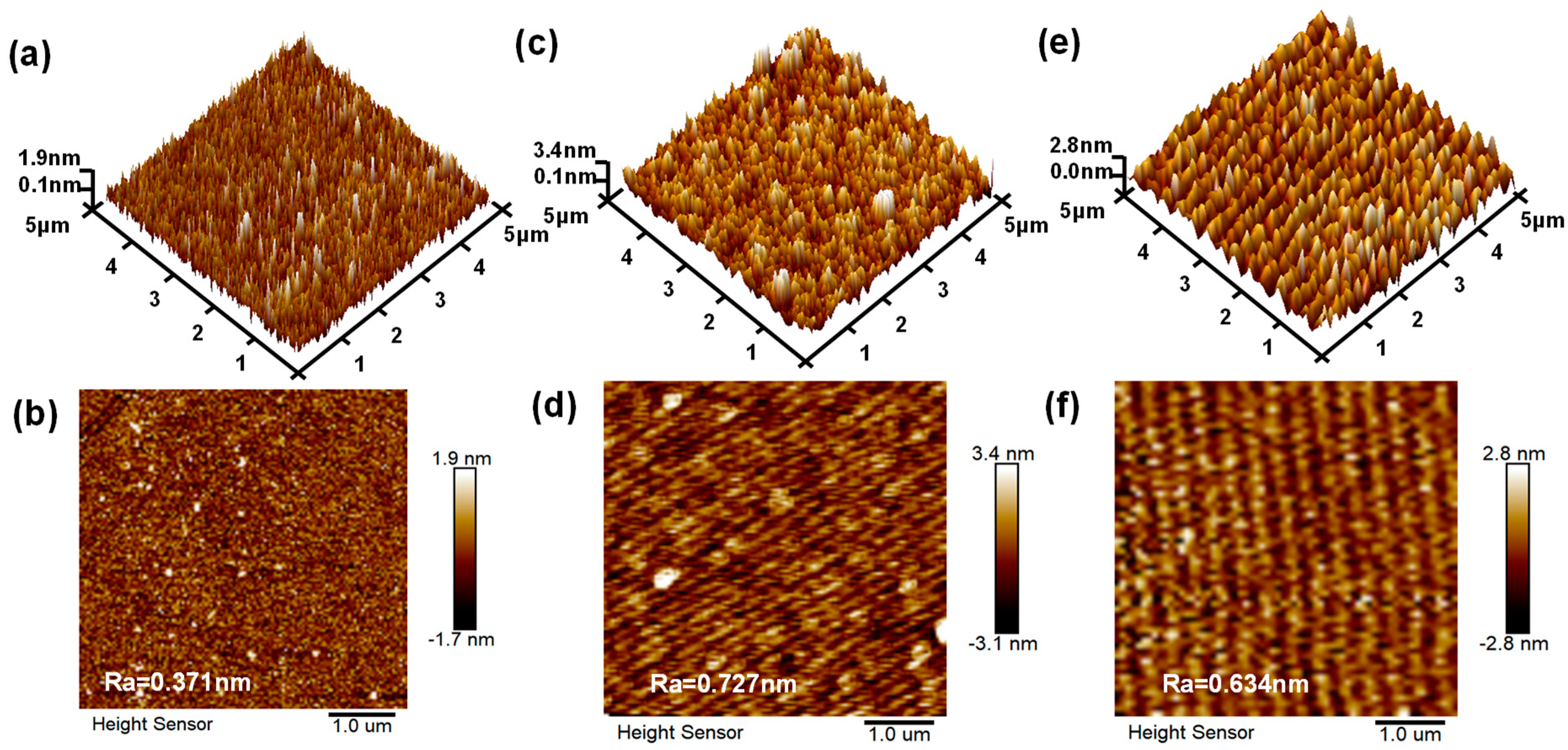
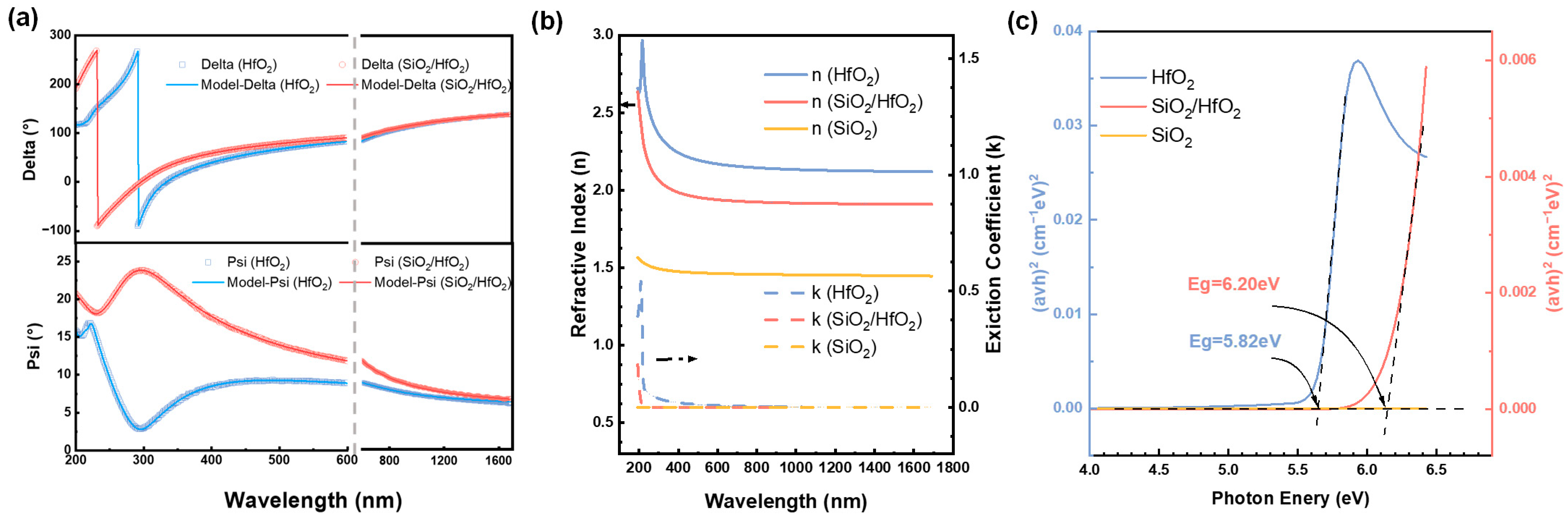
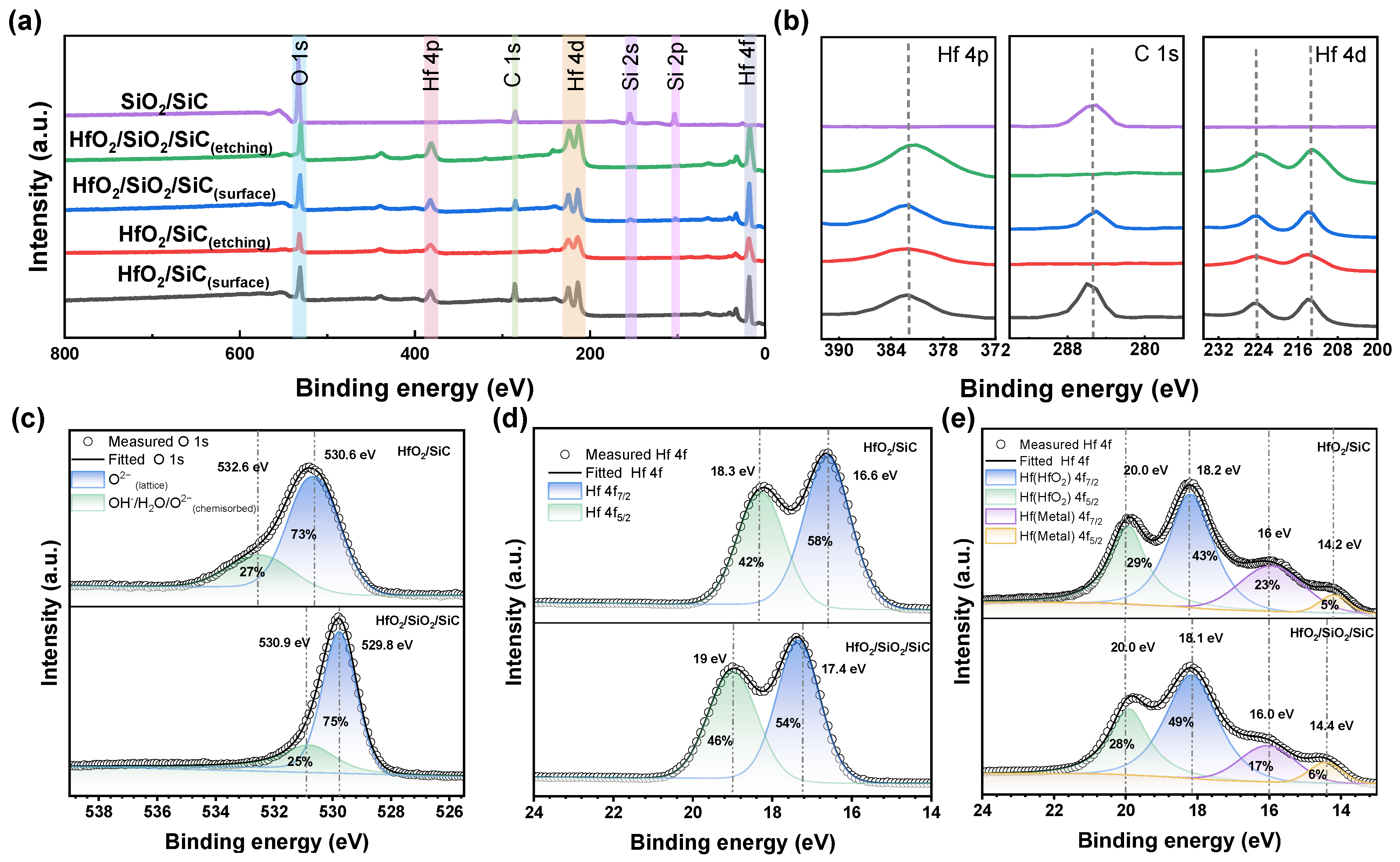
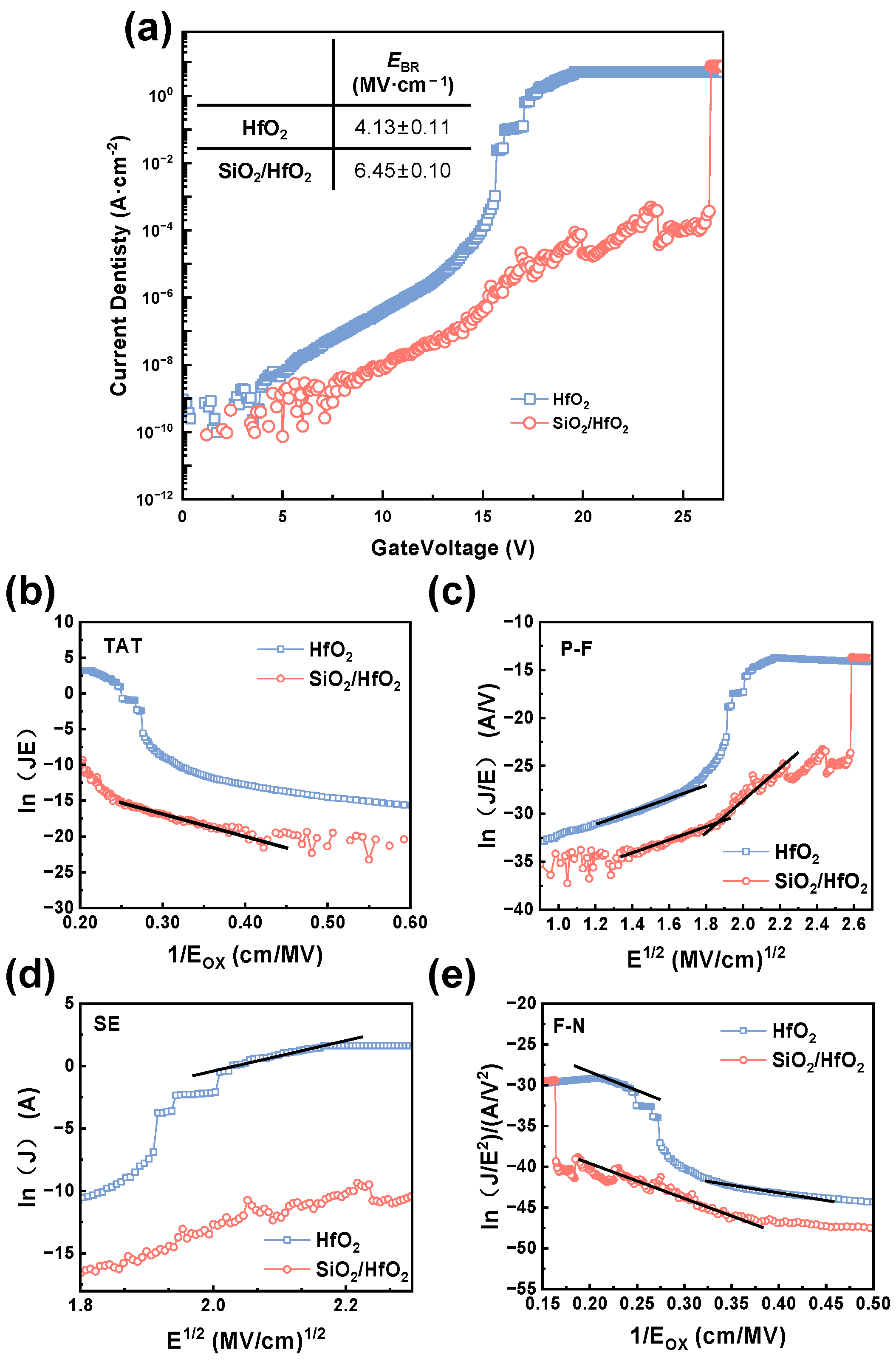
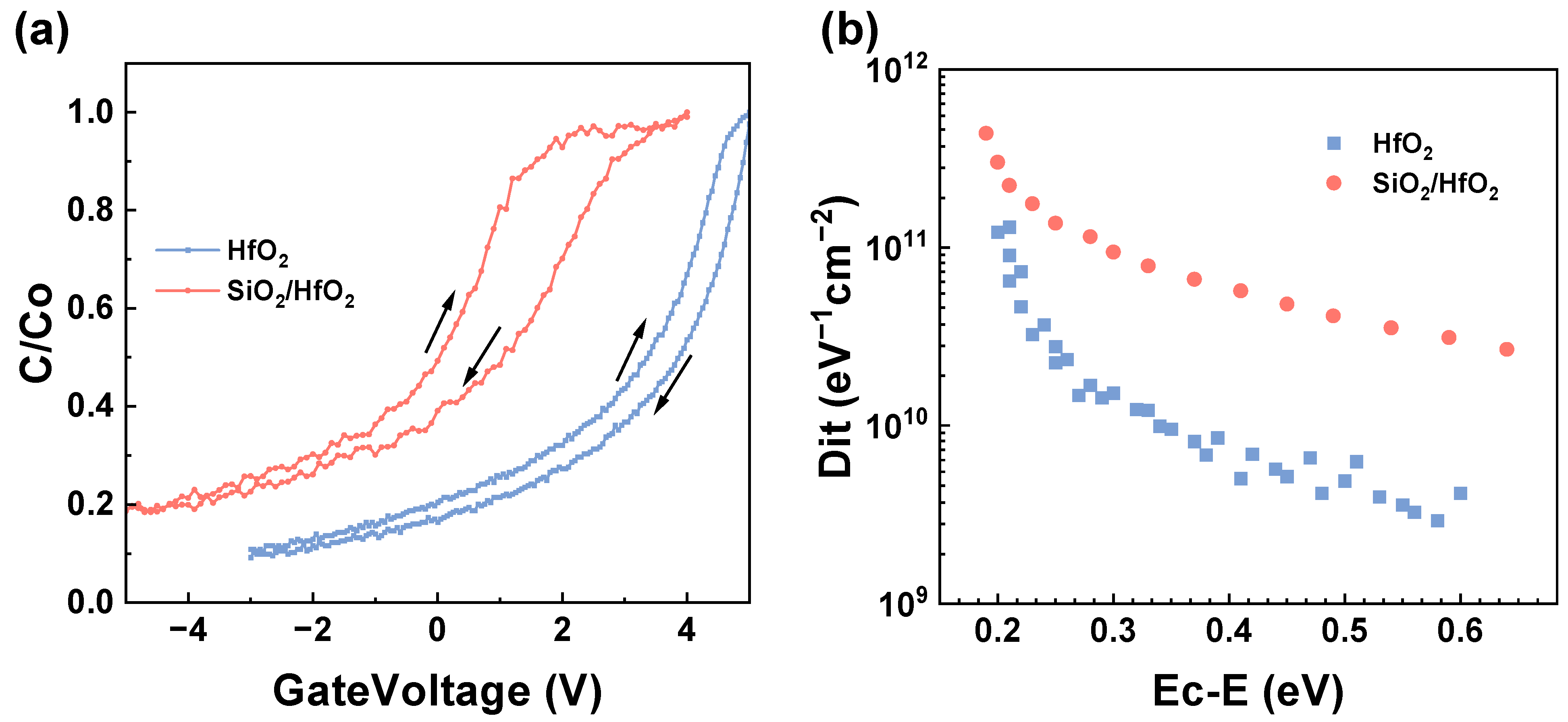
3. Results and Discussion

The surface morphologies and roughnesses of HfO2 and SiO2/HfO2 films samples and the interlayer SiO2 were characterized by AFM and the results are compared in Figure 3. The arithmetic mean roughness (Ra) was calculated based on a measured area of 5 × 5 µm2. Both surfaces remained relatively flat, with a determined Ra of 0.371 nm for HfO2 film and 0.727 nm for SiO2/HfO2 stacked film. Hence, the morphology and uniformity of films prepared by the ALD technique can be well controlled. However, the SiO2/HfO2 film exhibited comparatively higher surface roughness than HfO2, attributed to the different physical and chemical properties of SiO2 and HfO2 that may induce interfacial stress and defects during deposition to yield increased overall surface roughness. Furthermore, the multilayer structure may contribute since each added layer in the SiO2/HfO2 stack could introduce cumulative minor roughnesses, resulting in higher final surface roughness than the single HfO2 layer. In the SiO2/HfO2 stack structure, the presence of the SiO2 layer may introduce a slight increase in interface roughness. However, the surface roughnesses of both the HfO2 film and the SiO2/HfO2 stack remained at a low level overall.
A total of five point measurements were performed by SE at various locations of the films, and the mean values were calculated and used for analysis. The thickness of the HfO2 film was determined as 38.257 nm, while that of SiO2 and HfO2 layers in the SiO2/HfO2 composite film was estimated to be 10.73 nm and 29.78 nm, respectively. The measured psi(Ψ) and delta(Δ) curves are presented in Figure 4a, and the refractive index (n) and extinction coefficient (k) are given in Figure 4b. The absorption coefficient (α) was calculated by the following formula: α = 4πk/λ [22], where k is the extinction coefficient presented as a function of wavelength (λ), as shown in Figure 4c. The Tauc method was subsequently employed to plot the relationship between (αhυ)2 and photon energy (hυ) for extracting the optical bandgap through linear extrapolation [23]. From Figure 4, the optical bandgaps of HfO2 film and SiO2/HfO2 composite film were calculated as 5.82 eV and 6.20 eV, respectively [24]. Despite the low thickness of the introduced SiO2 film, its high bandgap width (approximately 9 eV) [25] allowed effective bandgap adjustment, conducive to breakdown voltage enhancement and leakage current reduction in the devices.
The elemental compositions and chemical states of the film surfaces were thoroughly investigated by XPS analysis. Figure 5a,b present the wide XPS spectra of HfO2 and SiO2/HfO2 dielectric surfaces before and after etching, as well as detailed spectra of the Hf 4p, C 1s, and Hf 4d peaks, including analysis of the SiO2 interlayer. The spectra displayed characteristic electron peaks of HfO2 corresponding to Hf 4f, Hf 4d, and Hf 4p [26], along with the XPS peaks of O 1s and C 1s. The comparison of HfO2 and SiO2/HfO2 films before and after etching revealed an increase in C 1s peak before etching, indicative of slight surface contamination. As shown in Figure 5b, the Hf 4d and Hf 4p peaks of both samples were identical.
The O 1s core-level XPS spectra and peak deconvolution of the HfO2 and SiO2/HfO2 films are illustrated in Figure 5c. The O 1s peak of the HfO2 film was divided into two peaks at 530.6 eV and 531.4 eV, while the O 1s peak of the SiO2/HfO2 film was split into two peaks at 529.4 eV and 530.5 eV. The Hf 4f core-level XPS spectra and peak separations of the surfaces of HfO2 and SiO2/HfO2 films in Figure 5d revealed well-separated Hf 4f7/2 and Hf 4f5/2 peaks by approximately 1.7 eV and 1.6 eV [27], respectively. The Hf 4f core-level XPS spectra and peak separations within the HfO2 and SiO2/HfO2 films are provided in Figure 5e. Besides the separation of the Hf 4f7/2 and Hf 4f5/2 peaks in HfO2, metallic Hf 4f7/2 and Hf 4f5/2 peaks were also observed [28], which may result from the reduction of HfO2 by high-energy ions during the etching process, forming metallic Hf. In the HfO2 film, the binding energies of the Hf 4f7/2 and Hf 4f5/2 peaks were estimated to be 18.2 eV and 20.0 eV, respectively. The area ratio of the Hf 4f7/2 to Hf 4f5/2 peaks in the HfO2 film was recorded as 43:29, while that of SiO2/HfO2 film was 49:28, with both values equivalent to a ratio of approximately 4:3 [28]. The latter would correspond to the occupancy levels caused by spin-orbit coupling, primarily determined by degeneracy.
The results of XPS indicated almost identical Hf 4f core levels in HfO2 and SiO2/HfO2 composite dielectrics, suggesting the negligible impact of the SiO2 interlayer and the SiC substrate on the electronic structure of the HfO2 film. This can be related to the characteristics of the ALD process, ensuring high uniformity and stability during the formation of interfacial layers for minimized interface effects. Furthermore, the previously mentioned energy bandgap (Eg) widening observed in the stacked samples is likely due to the presence of SiO2.
The electrical properties of the dielectrics were examined by testing the fabricated MOS capacitors with a probe station and a semiconductor analyzer. The current density (J)–voltage (V) characteristics of HfO2 and SiO2/HfO2 dielectric MOS capacitors are compared in Figure 6a, where J is normalized to the area of the square electrode and calculated by the following formula: J = I A , with I representing the measured current and A donating the electrode area [29]. As the electric field increased, the single-layer HfO2 capacitor exhibited a sudden jump in leakage current but without a significant breakdown phenomenon. After the breakdown, the current continued to rise, indicating a soft breakdown state. The breakdown voltage was estimated to be approximately 15.6 V, corresponding to a breakdown field of 4.1 MV/cm. For the stacked SiO2/HfO2 sample, the breakdown field at 26.3 V was calculated as 6.5 MV/cm, indicating a slightly improved breakdown field after the addition of the wide-bandgap dielectric SiO2 at the HfO2/SiC interface. The mean and standard deviation of the breakdown field for five sets of samples were calculated, as shown in the table in Figure 6a. For the single-layer HfO2, ION_EBR was determined as 1.1 × 10⁻³ A/cm2, whereas that of stacked SiO2/HfO2 was significantly lower (3.7 × 10⁻⁴ A/cm2). The leakage current and breakdown voltage increased after adding the SiO2 layer.
The conduction mechanisms under low leakage conditions were further analyzed using current density (J) – electric field (E) data extracted from experimental characteristics and used to construct conduction mechanism plots for different gate electric field regions [30,31]. Model parameters were extracted from the linear features of these plots and applied to simulate the analytical model equations for each conduction mechanism.
The gate leakage current in MOS capacitors would arise from various mechanisms, including direct tunneling (DT, path 1 in Figure 7), trap-assisted tunneling (TAT), Poole–Frenkel (P–F) emission, Schottky emission, and Fowler–Nordheim (F–N) tunneling. Since direct tunneling would typically occur in ultrathin dielectric layers, more focus was paid to TAT, P–F emission, Schottky emission, and F–N tunneling. The fitting results for different mechanisms based on the extracted parameters are presented in Figure 6b–e, and the model parameters and analytical equations for the mechanisms are listed in Table 1.
Trap-assisted tunneling (TAT), according to Path 2 in Figure 7, occurred when electrons first tunneled into traps within the dielectric thin film and then into the conduction band of the dielectric [32]. In Figure 6b, HfO2 displayed a lower trap density, resulting in a minimal contribution from the TAT mechanism. By contrast, the SiO2/HfO2 stack exhibited significant TAT activity due to the high-density traps introduced by the interface SiO2 layer. These traps captured and released electrons under low voltage, forming the TAT pathways.
Field-assisted thermal de-trapping of carriers from traps in the dielectric bulk into the conduction band resulted in P-F emission (path 3 in Figure 7) [34]. In Figure 3c, P–F emission primarily occurred under medium to high electric fields. Schottky emission (Path 4 in Figure 7) described the transition of electrons from a semiconductor into the conduction band of the insulating layer [34], a process analogous to thermionic emission in metal–semiconductor junctions. When the voltage rose to the medium field range, the P–F emission mechanism became active in the HfO2 film, releasing some electrons from the traps. In Figure 6d, the low barrier height simultaneously promoted the occurrence of Schottky emission. In the SiO2/HfO2 stack, the PF emission mechanism also became prominent and worked synergistically with TAT. However, the high barrier of the SiO2 layer suppressed Schottky emission, preventing its occurrence in this structure.
At higher gate voltages, electrons started to tunnel through a triangular potential barrier, resulting in F–N tunneling under high electric fields (Path 5 in Figure 7) [35]. As illustrated in Figure 6e, F–N tunneling dominated the current conduction in the HfO2 film at high fields, causing a rapid rise in current density. For the SiO2/HfO2 stack, the introduction of SiO2 significantly enhanced the barrier height, shifting the onset of F–N tunneling to higher electric fields. As a consequence, the increase in current was delayed when compared to pure HfO2 films. Additionally, even after the occurrence of hard breakdown in the HfO2 film, a portion of F–N tunneling persisted.
In sum, leakage current in the HfO2 film was primarily driven by P–F emission, Schottky emission, and F–N tunneling, while that of the SiO2/HfO2 stack was predominantly contributed by TAT, P–F emission, and F–N tunneling mechanisms.
The interface characteristics were examined by obtaining normalized C–V hysteresis curves of HfO2 and SiO2/HfO2 dielectric MOS capacitors measured at 1 MHz and the data are summarized in Figure 8a. Notably, the measurements were conducted with a 30 mV AC signal swept from negative to positive voltages and then returned from high to low voltages. The flat band voltage (VFB) was determined from the normalized capacitance of the MOS. The first step in this process consisted of calculating the flat band capacitance (CFB) using the following equation [36,37]:
C F B C o x = 1 1 + ε o x ε S i C t o x ε 0 ε S i C k T q 2 n 0
where Cox represents the oxide capacitance per unit area, tox is the thickness of the oxide layer, n0 denotes the majority carrier concentration in the epitaxial layer, and εox and εSiC are the relative permittivities of the oxide and SiC, respectively. For the SiO2/HfO2 stacked structure, the weighted average method was employed to account for the permittivity and thickness of both materials ( ε ox = d SiO 2 d total · ε SiO 2 + d HfO 2 d total · ε HfO 2 ) [38].
The calculated dielectric constant of the SiO2/HfO2 stack was approximately 16. The VFB values for the HfO2 and SiO2/HfO2 dielectric MOS capacitors were calculated as, respectively, 1.65 V and 0.8 V, showing significantly reduced flat-band voltage shift after the introduction of the SiO2 stack.
During high-frequency C–V testing, border traps cannot respond to small AC signal variations, but they can charge and discharge with the DC gate voltage sweep. Consequently, sweeping the gate voltage from negative to positive and from positive to negative during the test would result in hysteresis between the high-frequency dual C–V curves due to the presence of border trap charges. Since samples with stacked dielectrics exhibited larger hysteresis than the non-stacked HfO2 samples, it can be concluded that the HfO2 dielectric possessed relatively lower slow trap densities, which can be further demonstrated by calculating Dit.
As depicted in Figure 8b, the Dit calculated using the high-low-frequency method indicated a Dit value of 1.30 × 10¹¹ eV−1·cm−2 for HfO2 and 4.38 × 10¹¹ eV−1·cm−2 for SiO2/HfO2 stack at EC −0.2 eV. The SiO2/HfO2 bilayer films exhibited relatively high overall interface trap density, inferring the presence of certain defects and consistent with the TAT mechanism observed under medium electric fields. The higher interface trap density may also be attributed to the increased surface roughness of the SiO2/HfO2 bilayer. Also, elevated Dit values may be linked to the presence of defects introduced during the etching process, and interface quality might be improved through annealing treatments. However, overall, the Dit values of both samples remained in the same order of magnitude with minimal fluctuation.
The effective oxide charge (Neff) value in the oxide layer can be calculated using VFB [39,40]:
N e f f = ( W m W s q V F B ) · C o x
where Wm denotes the work function of Al metal (4.28 eV) and Ws is the work function of the semiconductor material.
The function of SiC can be calculated as follows:
W s = χ + E g 2 k T l n ( n 0 n i )
where χ, Eg, and ni are the electron affinity, bandgap, and intrinsic carrier concentration of SiC, respectively. Notably, W m W s q represents the ideal flat-band voltage without considering the charge in the oxide layer.
By substituting Equation (3) into Equation (2), the effective charge Neff can be obtained. The Neff values for HfO2 and SiO2/HfO2 dielectric MOS capacitors were recorded as −1.45 × 1011 cm−2 and −1.01 × 1011 cm−2, respectively. The electrical and interface characteristics of MOS capacitors based on HfO2 and SiO2/HfO2 dielectrics in Table 2 revealed negative Neff to cause a forward shift in the VFB. The Neff in the oxide layer consisted of Dit, fixed charge, oxide-trapped charge, and mobile charge [41]. These charges significantly impacted the electrical characteristics of trench MOSFETs, such as threshold voltage, flat-band voltage, and channel mobility. Therefore, the SiO2/HfO2 stacked structure improved the device’s interface quality by introducing a SiO2 interlayer able to reduce VFB shift and decrease the effective oxide charge.

4. Conclusions

In summary, ALD technology was successfully employed to grow HfO2 and SiO2/HfO2 gate dielectric films on etched 4H-SiC trench structures and fabricated corresponding MOS capacitors. The tests were conducted on a combined structure with both planar and vertical surfaces. AFM measurements showed that the roughness of both films was less than 1 nm, indicating relatively smooth surfaces. The test results showed HfO2 film exhibiting a breakdown electric field of 4.1 MV/cm with a leakage current of 1.1 × 10⁻³ A/cm2 at breakdown. By comparison, the SiO2/HfO2 film demonstrated a significantly higher breakdown electric field of 6.5 MV/cm and a much lower leakage current of 3.7 × 10⁻⁴ A/cm2. Leakage mechanism analysis revealed a leakage current in the HfO2 film, primarily driven by P–F emission, Schottky emission, and F–N tunneling, whereas the SiO2/HfO2 stack was dominated by TAT, P–F emission, and F–N tunneling. In the C-V hysteresis, a larger hysteresis was observed for the SiO2/HfO2 stacked dielectric, which is consistent with the increased roughness and Dit caused by the additional interface. However, the differences in roughness and Dit between the two samples were not significant, which can be attributed to the compact structure formed by the ALD process. The introduction of a thin SiO2 layer effectively solved the small bandgap offset, thereby increasing the bandgap from 5.82 eV to 6.20 eV and contributing to the reduction in leakage current. Furthermore, the etching process induced interface damage in the trench structure, potentially affecting device performance. Post-treatments could be considered to improve interface quality, which will be the focus of future research. Overall, the comprehensively analyzed performances of HfO2 and SiO2/HfO2 as gate dielectrics in 4H-SiC trench structures provide valuable references for future potential applications in 4H-SiC trench MOSFETs.

Author Contributions

Q.H.: methodology, data curation, formal analysis, writing—original draft. Y.G.: formal analysis, investigation, validation. A.W.: investigation, validation. L.G.: investigation, writing—review and editing. Z.W.: investigation. C.D.: validation, writing—review and editing. Y.S.: validation, writing—review and editing. H.M.: conceptualization, software, supervision, funding acquisition, project administration, writing—review and editing. Q.Z.: formal analysis, investigation, validation, supervision. All authors have read and agreed to the published version of the manuscript.

Funding

This work is supported by the National Key R&D Program of China (2023YFB4606300), the National Natural Science Foundation of China (No. 62474049), the Science and Technology Innovation Plan of Shanghai Science and Technology Commission (No. 21DZ1100800, 23ZR1405300, 20501110700, and 20501110702), and the Joint Research Plan of the sci-tech innovation community in the Yangtze River Delta (No. 2023CSJG0600).

Data Availability Statement

The original contributions presented in this study are included in the article. Further inquiries can be directed to the corresponding author.

Conflicts of Interest

The authors declare that they have no known competing financial interests or personal relationships that could have appeared to influence the work reported in this paper.

References

  1. Baliga, B.J. Fundamentals of Power Semiconductor Devices; Springer Nature: Cham, Switzerland, 2019. [Google Scholar]
  2. Kimoto, T. Material Science and Device Physics in SiC Technology for High-Voltage Power Devices. Jpn. J. Appl. Phys. 2015, 54, 040103. [Google Scholar] [CrossRef]
  3. Jayant Baliga, B. Silicon Carbide Power Devices: Progress and Future Outlook. IEEE J. Emerg. Sel. Top. Power Electron. 2023, 11, 2400–2411. [Google Scholar] [CrossRef]
  4. Kimoto, T. SiC Material Properties. In Wide Bandgap Semiconductor Power Devices; Woodhead Publishing: Cambridge, UK, 2019; pp. 21–42. ISBN 9780081023068. [Google Scholar]
  5. Qian, J.; Shi, L.; Jin, M.; Bhattacharya, M.; Shimbori, A.; Yu, H.; Houshmand, S.; White, M.H.; Agarwal, A.K. An Investigation of Body Diode Reliability in Commercial 1.2 KV SiC Power MOSFETs with Planar and Trench Structures. Micromachines 2024, 15, 177. [Google Scholar] [CrossRef] [PubMed]
  6. Siddiqui, A.; Khosa, R.Y.; Usman, M. High-K Dielectrics for 4H-Silicon Carbide: Present Status and Future Perspectives. J. Mater. Chem. C 2021, 9, 5055–5081. [Google Scholar] [CrossRef]
  7. Cheon, J.; Kim, K. Numerical Simulation Analysis of Switching Characteristics in the Source-Trench MOSFET’s. Electronics 2020, 9, 1895. [Google Scholar] [CrossRef]
  8. Wirths, S.; Mihaila, A.; Romano, G.; Schneider, N.; Ceccarelli, E.; Alfieri, G.; Arango, Y.; Knoll, L. Study of 1.2kV High-k SiC Power MOSFETS under Harsh Repetitive Switching Conditions. In Proceedings of the 2021 33rd International Symposium on Power Semiconductor Devices and ICs (ISPSD), Nagoya, Japan, 30 May–3 June 2021; pp. 107–110. [Google Scholar] [CrossRef]
  9. Race, S.; Kumar, P.; Natzke, P.; Kovacevic-Badstuebner, I.; Bathen, M.E.; Grossner, U.; Romano, G.; Arango, Y.; Bolat, S.; Wirths, S.; et al. Gate Impedance Analysis of SiC Power MOSFETs with SiO2 and High-k Dielectric. In Proceedings of the 2023 35th International Symposium on Power Semiconductor Devices and ICs (ISPSD), Hong Kong, China, 28 May–1 June 2023. [Google Scholar] [CrossRef]
  10. Takaya, H.; Misumi, T.; Fujiwara, H.; Ito, T. 4H-SiC Trench MOSFET with Low On-Resistance at High Temperature. In Proceedings of the 2020 32nd International Symposium on Power Semiconductor Devices and ICs (ISPSD), Vienna, Austria, 13–18 September 2020; pp. 118–121. [Google Scholar] [CrossRef]
  11. Wei, J.; Wei, Z.; Fu, H.; Cao, J.; Wu, T.; Sun, J.; Zhu, X.; Li, S.; Zhang, L.; Liu, S.; et al. Review on the Reliability Mechanisms of SiC Power MOSFETs: A Comparison between Planar-Gate and Trench-Gate Structures. IEEE Trans. Power Electron. 2023, 38, 8990–9005. [Google Scholar] [CrossRef]
  12. Hsu, C.-M.; Hwu, J.-G. Investigation of Carbon Interstitials with Varied SiO2 Thickness in HfO2/SiO2/4H-SiC Structure. Appl. Phys. Lett. 2012, 101, 253517. [Google Scholar] [CrossRef]
  13. Boccarossa, M.; Maresca, L.; Borghese, A.; Riccio, M.; Breglio, G.; Irace, A.; Salvatore, G.A. Substantial Improvement of the Short-Circuit Capability of a 1.2 KV SiC MOSFET by a HfO2/SiO2 Ferroelectric Gate Stack. In Proceedings of the 2024 36th International Symposium on Power Semiconductor Devices and ICs (ISPSD), Bremen, Germany, 2–6 June 2024; pp. 88–91. [Google Scholar] [CrossRef]
  14. Behera, M.K.; Yarbrough, K.A.; Bahoura, M. Study of Dielectric Properties in Stacked High-k Dielectric Metal Oxide Semiconductor Capacitor (MOSCAP) Devices. J. Mater. Sci. Mater. Electron. 2024, 35, 1316. [Google Scholar] [CrossRef]
  15. Cheong, K.Y.; Moon, J.H.; Park, T.J.; Kim, J.H.; Hwang, C.S.; Kim, H.J.; Bahng, W.; Kim, N.-K. Improved Electronic Performance of HfO2/SiO2 Stacking Gate Dielectric on 4H SiC. IEEE Trans. Electron Devices 2007, 54, 3409–3413. [Google Scholar] [CrossRef]
  16. Wang, Z.; Zhang, Z.; Shao, C.; Robertson, J.; Liu, S.; Guo, Y. Tuning the High-κ Oxide (HfO2, ZrO2)/4H-SiC Interface Properties with a SiO2 Interlayer for Power Device Applications. Appl. Surf. Sci. 2020, 527, 146843. [Google Scholar] [CrossRef]
  17. Zanders, D.; Ciftyurek, E.; Subaşı, E.; Huster, N.; Bock, C.; Kostka, A.; Rogalla, D.; Schierbaum, K.; Devi, A. PEALD of HfO2 Thin Films: Precursor Tuning and a New Near-Ambient-Pressure XPS Approach to in Situ Examination of Thin-Film Surfaces Exposed to Reactive Gases. ACS Appl. Mater. Interfaces 2019, 11, 28407–28422. [Google Scholar] [CrossRef] [PubMed]
  18. Guo, Z.; Wu, J.; Tian, R.; Wang, F.; Xu, P.; Yang, X.; Fan, Z.; Yang, F.; He, Z. Extraction of the Trench Sidewall Capacitances in an N-Type 4H-SiC Trench Metal– Oxide–Semiconductor Structure. IEEE Trans. Electron Devices 2021, 68, 2879–2885. [Google Scholar] [CrossRef]
  19. Cheong, K.Y.; Moon, J.H.; Kim, H.J.; Bahng, W.; Kim, N.K. Current Conduction Mechanisms in Atomic-Layer-Deposited HfO2/Nitrided SiO2 Stacked Gate on 4H Silicon Carbide. J. Appl. Phys. 2008, 103, 084113. [Google Scholar] [CrossRef]
  20. Giannazzo, F.; Schilirò, E.; Lo Nigro, R.; Roccaforte, F.; Yakimova, R. Atomic Layer Deposition of High-k Insulators on Epitaxial Graphene: A Review. Appl. Sci. 2020, 10, 2440. [Google Scholar] [CrossRef]
  21. Liang, L.; Li, W.; Li, S.; Li, X.; Wu, Y. Interface Properties Study on SiC MOS with High-k Hafnium Silicate Gate Dielectric. AIP Adv. 2018, 8, 125314. [Google Scholar] [CrossRef]
  22. Fowler, R.H.; Nordheim, L. Electron Emission in Intense Electric Fields. Proc. R. Soc. Lond. Ser. A Contain. Pap. A Math. Phys. Character 1928, 119, 173–181. [Google Scholar] [CrossRef]
  23. Nguyen, T.T.; Jung, D.H.; Lee, J.J.; Lee, H. Optical Study of Ga2-XSnxO3 (0 ≤ X ≤ 0.7) Thin Films Using Spectroscopic Ellipsometry and Cathodoluminescence. Thin Solid Films 2023, 764, 139611. [Google Scholar] [CrossRef]
  24. Sahoo, G.S.; Tripathy, S.P.; Joshi, D.S.; Kulkarni, M.S. Development of an Algorithm for Precise and Automated Determination of Optical Band Gap from Tauc Analysis: Case Studies Using Alpha-Irradiated CR-39 Detectors. Radiat. Eff. Defects Solids 2020, 175, 1127–1139. [Google Scholar] [CrossRef]
  25. Haider, M.; Shaim, A.; Elsayed-Ali, H.E. Boron and Barium Incorporation at the 4H-SiC/SiO2 Interface Using a Laser Multi-Charged Ion Source. J. Mater. Sci. Mater. Electron. 2021, 32, 16079–16087. [Google Scholar] [CrossRef]
  26. Kumar, M.; Singh, R.P.; Kumar, A. Opto-Electronic Properties of HfO2: A First Principle-Based Spin-Polarized Calculations. Optik 2020, 226, 165937. [Google Scholar] [CrossRef]
  27. Huang, H.; Wang, Y.; Chen, K.-H.; Fei, X.-X. Leakage Current Behavior in HfO2/SiO2/al2O3 Stacked Dielectric on 4H-SiC Substrate. IEEE J. Electron Devices Soc. 2023, 11, 438–443. [Google Scholar] [CrossRef]
  28. Renault, O.; Samour, D.; Damlencourt, J.-F.; Blin, D.; Martin, F.; Marthon, S.; Barrett, N.T.; Besson, P. HfO2/SiO2 Interface Chemistry Studied by Synchrotron Radiation X-Ray Photoelectron Spectroscopy. Appl. Phys. Lett. 2002, 81, 3627–3629. [Google Scholar] [CrossRef]
  29. Lee, T.-E.; Toprasertpong, K.; Takenaka, M.; Takagi, S. Re-Examination of Effects of ALD High-k Materials on Defect Reduction in SiGe Metal–Oxide–Semiconductor Interfaces. AIP Adv. 2021, 11, 085021. [Google Scholar] [CrossRef]
  30. Chand, U.; Bera, L.K.; Singh, N.; Zhixian, C.; Kumar, S.; Voo, Q.G.R.; Yeo, A.H.; Varghese, B.; Reddy, V.P.; Cakmak, H.; et al. High-K Gate Dielectric for High-Performance SiC Power MOSFET Technology with Low Interface Trap Density, Good Oxide Lifetime (Ttddb≥ 104S), and High Thermal Stability (≥ 800 °C). Diffus. Defect Data Solid State Data Part B Solid State Phenom./Solid State Phenom. 2024, 359, 217–221. [Google Scholar] [CrossRef]
  31. Esakki, P.; Kailath, B.J. Extraction and Analysis of Gate Leakage Current Mechanism in Silicon Carbide (SiC) MIS Capacitors. IETE J. Res. 2019, 68, 592–601. [Google Scholar] [CrossRef]
  32. Ouennoughi, Z.; Strenger, C.; Bourouba, F.; Haeublein, V.; Ryssel, H.; Frey, L. Conduction Mechanisms in Thermal Nitride and Dry Gate Oxides Grown on 4H-SiC. Microelectron. Reliab. 2013, 53, 1841–1847. [Google Scholar] [CrossRef]
  33. Cheong, K.Y.; Bahng, W.; Kim, N.-K. Analysis of Charge Conduction Mechanisms in Nitrided SiO2 Film on 4H SiC. Phys. Lett. A 2008, 372, 529–532. [Google Scholar] [CrossRef]
  34. Kuang, N.Q.; Liu, N.H.; Zhou, N.W.; Gao, N.B.; Zhao, A.; Tallavarjula, S. Transport Mechanism of the Leakage Current in MIS Capacitor with HfO2/SiO2 Stack Gate. In Proceedings of the 2009 IEEE International Conference of Electron Devices and Solid-State Circuits (EDSSC), Xi’an, China, 25–27 December 2009; Volume 25, pp. 229–232. [Google Scholar] [CrossRef]
  35. Shi, L.; Qian, J.; Jin, M.; Bhattacharya, M.; Houshmand, S.; Yu, H.; Shimbori, A.; White, M.H.; Agarwal, A.K. Gate Oxide Reliability in Silicon Carbide Planar and Trench Metal-Oxide-Semiconductor Field-Effect Transistors under Positive and Negative Electric Field Stress. Electronics 2024, 13, 4516. [Google Scholar] [CrossRef]
  36. Wang, X.; Wei, S.; Ke, H.; Ye, X.; Weng, H.; Wong, S.Y.; Yang, W. Simultaneous Electric Dipoles and Flat-Band Voltage Modulation in 4H-SiC MOS Capacitors through HfO2/SiO2 Interface Engineering. J. Phys. D Appl. Phys. 2024, 57, 37LT01. [Google Scholar] [CrossRef]
  37. Guo, Z.; He, Z.; Wang, F.; Wu, J.; Yang, X.; Fan, Z.; Yang, F. Study of Vertical Capacitance in an N-Type 4H-SiC Stepped Thick-Oxide Trench MOS Structure. IEEE Trans. Electron Devices 2022, 69, 4617–4623. [Google Scholar] [CrossRef]
  38. Galizia, B.; Fiorenza, P.; Schilirò, E.; Pecz, B.; Foragassy, Z.; Greco, G.; Saggio, M.; Cascino, S.; Lo Nigro, R.; Roccaforte, F. Towards Aluminum Oxide/Aluminum Nitride Insulating Stacks on 4H–SiC by Atomic Layer Deposition. Mater. Sci. Semicond. Process. 2024, 174, 108244. [Google Scholar] [CrossRef]
  39. Jia, Y.; Lv, H.; Tang, X.; Han, C.; Song, Q.; Zhang, Y.; Zhang, Y.; Dimitrijev, S.; Han, J.; Haasmann, D. Influence of Various NO Annealing Conditions on N-Type and P-Type 4H-SiC MOS Capacitors. J. Mater. Sci. Mater. Electron. 2019, 30, 10302–10310. [Google Scholar] [CrossRef]
  40. Yang, C.; Huang, H.; Peng, M. Non-Iterative Method for Extracting Complex Permittivity and Thickness of Materials from Reflection-Only Measurements. IEEE Trans. Instrum. Meas. 2022, 71, 1–8. [Google Scholar] [CrossRef]
  41. Martínez-Puente, M.A.; Horley, P.; Aguirre-Tostado, F.S.; López-Medina, J.; Borbón-Núñez, H.A.; Tiznado, H.; Susarrey-Arce, A.; Martínez-Guerra, E. ALD and PEALD Deposition of HfO2 and Its Effects on the Nature of Oxygen Vacancies. Mater. Sci. Eng. B 2022, 285, 115964. [Google Scholar] [CrossRef]
Figure 1. (a) Schematic diagram of manufacturing process flow for trench MOS and (b) scheme of the final fabricated sample structure.
Nanomaterials 15 00343 g001
Figure 2. SEM images (a) after SiO2 etching, (b) after SiC etching, (c) of the trench structure after BOE cleaning, (d) after ALD processing, and (e) of magnification of the white-boxed area in (d).
Nanomaterials 15 00343 g002
Figure 3. Both 3D and 2D AFM images within the area of 5 × 5 um2 for (a,b) HfO2 and (c,d) SiO2/HfO2, and (e,f) interlayer SiO2.
Nanomaterials 15 00343 g003
Figure 4. SE results for HfO2 and SiO2/HfO2 samples: (a) Ψ (psi) and Δ (delta) of the measured complex reflectance, (b) fitted refractive index and extinction coefficient, and (c) (αhν)2 parameter versus photon energy for the fitted bandgap.
Nanomaterials 15 00343 g004
Figure 5. (a) XPS spectra of HfO2 and SiO2/HfO2 sample surfaces and the etched and interlayer SiO2, (b) O 1s core level, (c) sample surface, (d) etched Hf 4f core level, and (e) magnified view of Hf 4p, C 1s, and Hf 4d peaks.
Nanomaterials 15 00343 g005
Figure 6. (a) Current density (J)-voltage (V) curves of MOS capacitors. Electric fields of HfO2 and SiO2/HfO2 dielectric MOS capacitors for (b) TAT, (c) Frenkel–Poole emission, (d) Schottky emission, and (e) F–N tunneling model fitting plot.
Nanomaterials 15 00343 g006
Figure 7. Schematic energy-band diagrams of (a) HfO2 and (b) SiO2/HfO2 MOS structures. The numbering 1–5 refers to respective leakage paths due to direct tunneling, trap-assisted tunneling, Poole–Frenkel emission, Schottky emission, and Fowler–Nordheim tunneling. EC, EF, EV, and EFM are the conduction band edge, Fermi level, valence band edge, and Fermi level of Al, respectively.
Nanomaterials 15 00343 g007
Figure 8. (a) Normalized C-V hysteresis curves of MOS capacitors with HfO2 and SiO2/HfO2 dielectrics, and (b) calculated interface trap density Dit plots.
Nanomaterials 15 00343 g008
Table 1. Conduction plots and analytical model equations of different gate leakage current mechanisms.
Conduction MechanismsConduction PlotAnalytical Model Equations
TATln( J E ) ∝ 1 E J T A T = 2 q c T N T ϕ T exp D ϕ T 3 2 E o x 3 E o x [32]
P–F emissionln( J E ) ∝ E J P F = q N c μ E o x exp q ϕ t q E o x π ε 0 k r k T [18]
Schottky emissionln( J ) ∝ E J S E = A * T 2 exp q ϕ B q E o x 4 ε o x k T [18]
F–N tunnelingln( J E 2 ) ∝ 1 E J F N = A E o x 2 exp B E o x [33]
Table 2. Electrical and interface characteristics of MOS capacitors based on HfO2 and SiO2/HfO2 dielectrics.
Stack InformationVFB (V)EBR (MV·cm−1)ION_EBR (A·cm−2)Dit (eV−1·cm−2)
EC-0.2 eV
Neff (cm−2)
HfO21.654.11.1 × 10−31.30 × 10¹¹−1.45 × 10¹¹
SiO2/HfO20.86.53.7 × 10−44.38 × 10¹¹−1.01 × 10¹¹
Disclaimer/Publisher’s Note: The statements, opinions and data contained in all publications are solely those of the individual author(s) and contributor(s) and not of MDPI and/or the editor(s). MDPI and/or the editor(s) disclaim responsibility for any injury to people or property resulting from any ideas, methods, instructions or products referred to in the content.

