Communication

Controlled Vapor-Phase Synthesis of VSe2 via Selenium-Driven Gradual Transformation of Single-Crystalline V2O5 Nanosheets

Department of Electronic Engineering, Gachon University, Seongnam 13120, Republic of Korea
Nanomaterials 2025, 15(7), 548; https://doi.org/10.3390/nano15070548
Submission received: 13 March 2025 / Revised: 28 March 2025 / Accepted: 1 April 2025 / Published: 4 April 2025
(This article belongs to the Section Synthesis, Interfaces and Nanostructures)

Abstract

:
We report a gas-phase precursor modulation strategy for the controlled synthesis of 1T-phase vanadium diselenide (VSe2) from vanadium pentoxide (V2O5) nanosheets by systematically adjusting the vapor pressure of selenium. By controlling the selenium vapor pressure, selenium-free vapor transport of vanadium dioxide led to the spontaneous oxidation and formation of tens-of-micrometer-sized rectangular V2O5 crystals, while moderate selenium introduction produced intermediate oxygen-rich phases with trapezoidal crystal facets, and a highly selenium-rich environment yielded trigonal VSe2 crystals. Raman scattering measurements confirmed the stepwise transformation from V2O5 to VSe2, and atomic force microscopy revealed well-defined layered morphologies and distinct conformation within an atomically thin regime. Additionally, high-resolution transmission electron microscopy validated the orthorhombic and trigonal crystal structures of V2O5 and VSe2, respectively. This work demonstrates the versatility of fine-tuned vapor-phase growth conditions in vanadium-based layered compounds, providing useful platforms to optimize structural composition with atomic precision.

1. Introduction

Nanostructured transition metal dichalcogenides (TMDCs) with two-dimensional (2D) layered structures have attracted substantial interest due to their unique electronic, optical, and catalytic properties. These materials exhibit exotic phenomena, such as charge density waves (CDWs), superconductivity, and phase transitions, making them attractive for future computing applications, including field-effect transistors, optoelectronic devices, and energy storage systems [1,2,3,4,5,6,7,8,9,10,11,12,13,14,15,16]. Among TMDCs, vanadium diselenide (VSe2) stands out because of its intriguing physical properties. In its 1T phase, VSe2 is metallic and exhibits a CDW transition at low temperatures below ~110 K. Despite the promises for potential applications such as in memristor and neuromorphic hardware, the electronic structure of 1T VSe2 is often sensitive to external factors such as air exposure and point defects, requiring thorough understanding of its synthesis protocol with controlled stoichiometry and composition [17,18,19,20]. Meanwhile, vanadium pentoxide (V2O5), a dissimilar layered vanadium compound, is widely utilized in electrochemical energy storage, catalysis, and optoelectronics [21,22,23,24,25,26,27,28]. It possesses a stable orthorhombic crystal structure and a high oxidation state of vanadium, making it a suitable template for transformation into lower-oxidation-state vanadium chalcogenides [29,30,31]. The precision transformation from atomically thin V2O5 to VSe2 involves the reduction of vanadium and the incorporation of selenium, leading to versatile material platforms.
Here, we demonstrated a vapor-phase synthesis approach for VSe2 through the selenium-induced transformation of single-crystalline V2O5 nanosheets. By precisely tuning the selenium vapor pressure, we directed the stepwise transformation from V2O5 to VSe2 via intermediate oxygen-rich vanadium selenide phases. Our findings offer insights into the role of precursor modulation in TMDC growth and pave the way for designing high-quality layered materials with tailored electronic properties.

2. Results and Discussion

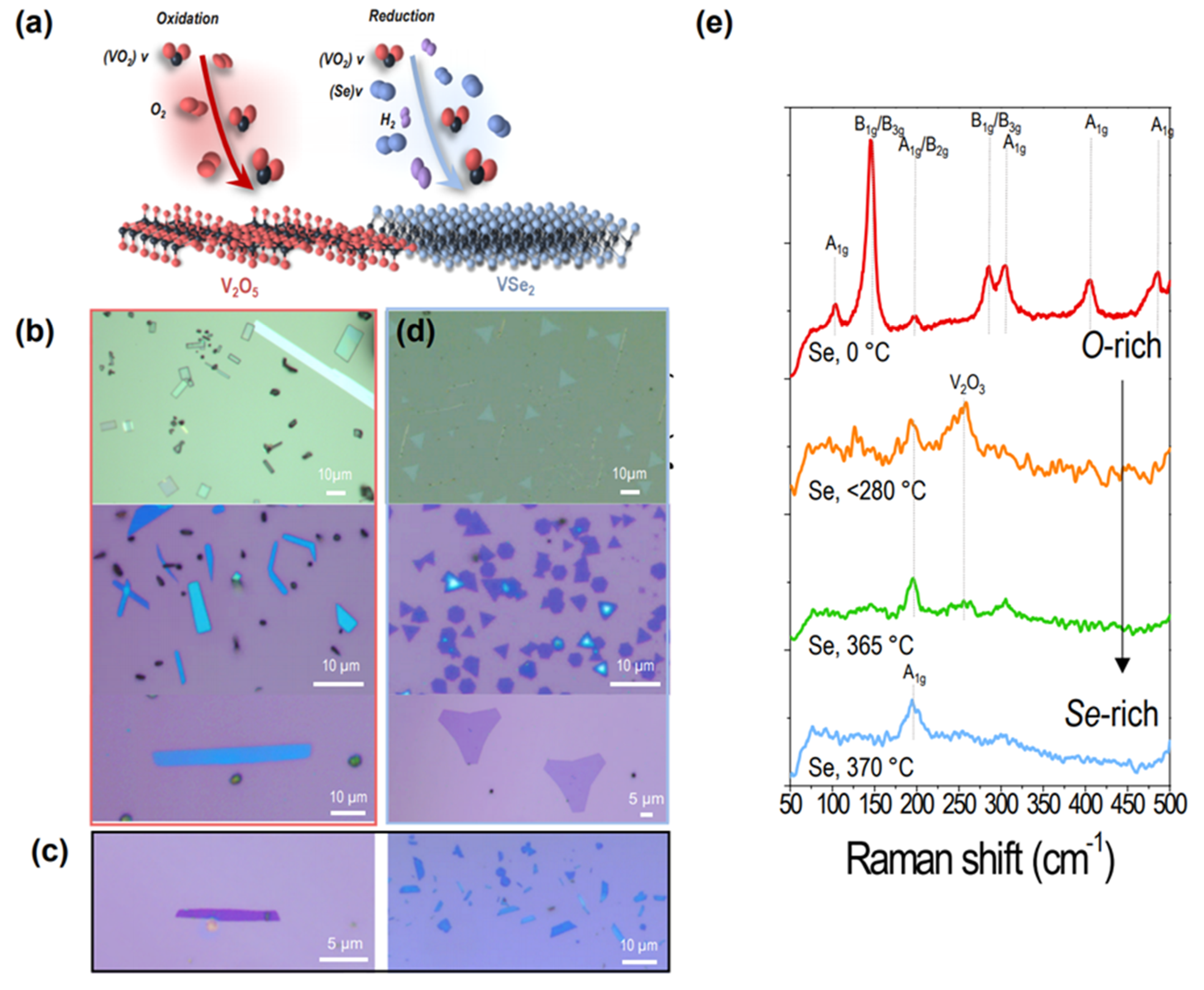
2.1. Vapor-Phase Control of Selenium for Synthesis of O-Rich and Se-Rich Crystals

The controlled synthesis of VSe2 was achieved by progressive precursor modulation, increasing the vapor pressure of selenium and maintaining that of VO2 (Figure 1a). First, in the absence of selenium, rutile VO2 was synthesized in a chemical vapor deposition system. Layered V2O5 nanosheets with a lateral size of tens of micrometers were grown by the spontaneous oxidation of VO2 vapor, forming rectangular-faceted single crystals (Figure 1b), presumably due to diffusion-limited growth, where oxygen diffusion to the surface controlled the rate of oxidation. Ar/H2 mixture gas also acted as a reductant, helping to reduce VO2 towards a lower oxidation state. Then, the selenium-driven transformation of V2O5 nanosheets was achieved by introducing the vapor pressure of selenium (280~370 °C) and maintaining other growth parameters (total pressure, amount of precursor powder, flow rate of Ar/H2) during the reactions, resulting in the gradual modification of facets from rectangles to trapezoids, as shown in Figure 1c. We identified these crystals as intermediate states between V2O5 and VSe2. Under the selenium-rich environment (selenium at 370 °C), trigonal VSe2 crystals revealed triangular facets on sapphire substrate (top) and SiO2 substrates (bottom) (Figure 1d), highlighting a complete transformation. The gradual transformation was may attributed to the vapor pressure of selenium gradually substituting the oxygen atoms within the lattice, thereby modifying the vanadium oxidation state. This gradual transformation from V2O5 to VSe2 was verified by Raman characterization. To confirm the gradual transformation with consistency, Raman scattering spectra (Figure 1d) were measured from four individual batches. With considerable Se addition, a dramatic change in the peak positions was also identified via Raman spectroscopy (Figure 1e and Table 1). Under the growth condition without selenium vapor, which was not heated in a separate zone, the rectangular crystal showed seven prominent scattering peaks [103.7 cm−1 (A1g), 145.6, 284.7 cm−1 (B1g/B3g), 196.8 cm−1 (A1g/A2g), 304.4, 405.4, and 484.1 cm−1 (A1g)]. Under the condition with selenium at <280 °C, those peaks were not noticeable, showing new peaks at ~255 cm−1, which was attributed to V2O3, and 195 cm−1, indicative of an intermediate selenization stage. Sufficient amounts of Se at 365~370 °C resulted in a clear peak of A1g (200.6 cm−1) vibration modes, confirming the formation of trigonal VSe2.

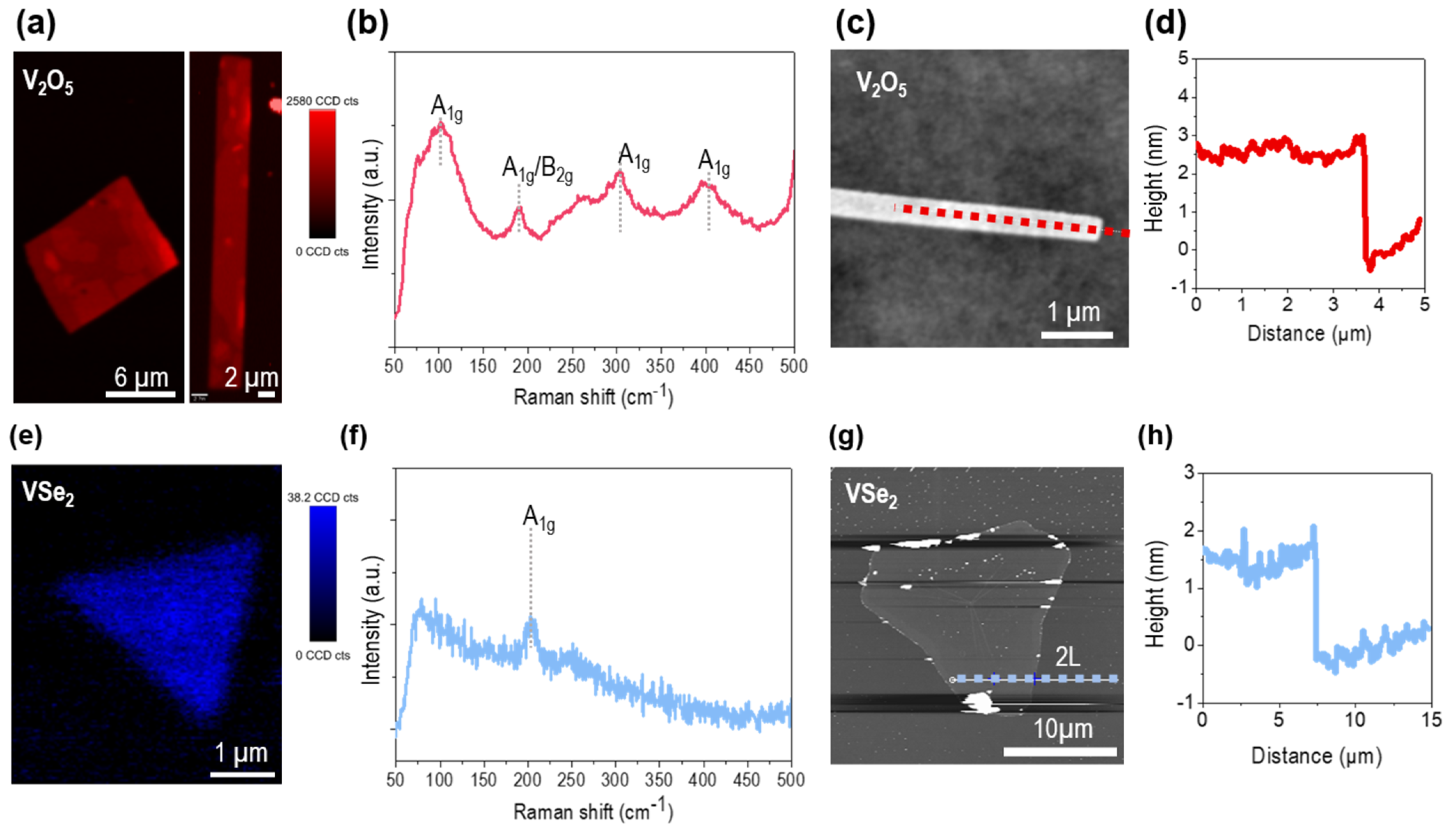
2.2. Material Characterization of Atomically Thin VSe2 and V2O5 Nanosheets

Se-rich and O-rich vanadium compounds were further optimized to thin down the thickness of the crystals. Alkali halide (potassium iodide) was introduced to act as a nucleation inhibitor to suppress the nucleation density. The alkali halide is known for its function as a surfactant, reducing surface energy and thereby limiting excessive nucleation events. To characterize the atomically thin nanosheets of VSe2 and V2O5 obtained under two different conditions using the controlled vaporization of selenium, we performed Raman mapping at a wavelength of 532 nm. In Figure 1a, a rectangular crystal with additional vertically overgrown layers is revealed in the Raman mapping images. This crystal showed four Raman peaks (102.3 cm−1, 190.2 cm−1, 303.2 cm−1, and 401.5 cm−1), as shown in Figure 2b, which were partially red-shifted, as indexed in Table 1 [32,33]. These V2O5 nanosheets were characterized by atomic force microscopy (Figure 2c), displaying clean surface and edges in the AFM scan images even at a thickness of 3 nm. Atomically thin VSe2 showed weak intensities in the Raman mapping image (Figure 2e). It had a sole vibration mode at ~206 cm−1 that was blue-shifted, indicating a reduced layer thickness compared to the reference bulk crystals. The surface of VSe2 was contaminated, as we observed oxidized chunks at the crystal edges in the AFM mapping image with the step height of a bilayer.

2.3. Crystal Structure of Orthorhombic V2O5 and Trigonal VSe2

The atomic structures of the VSe2 and V2O5 were characterized by transmission electron microscopy (TEM). Due to the inability to transfer V2O5 grown on SiO2 substrates using hydrofluoric acid or potassium hydroperoxide etching, the focused ion beam (FIB) was exploited to pick up V2O5/SiO2 stacks. The prepared V2O5 specimen had an orthorhombic crystal structure, which was classified as a Pmmn space group, as shown in Figure 3a. The plan-view V2O5 showed rectangular atomic arrangements with corresponding (020) diffraction spots, as shown in the selected-area electron diffraction (SAED) pattern in Figure 3b,c, although vanadium atoms were only attributed to this TEM image. Additionally, high-resolution bright-field TEM indicated that VSe2 multilayers (Figure 3d) exhibited a trigonal structure with (10-10) diffraction spots (Figure 3e,f) despite the substantial contamination along the edges of the crystal that was observed in the AFM scan image [20]. The observed diffraction patterns confirmed the integrity of the synthesized layers, with no detectable alloying effects between VSe2 and V2O5.

3. Materials and Methods

3.1. Chemical Vapor Deposition (CVD) of Atomically Thin Vanadium Compounds

The synthesis of V2O5 and VSe2 was carried out using a CVD approach. V2O5 nanosheets were synthesized via the vapor-phase oxidation of vanadium dioxide (VO2). High-purity VO2 powder (99.99%) was placed in a ceramic boat at the center of a 3 in. quartz tube furnace, and a 1 cm × 1 cm sapphire or 2 cm × 2 cm SiO2/Si substrate was positioned downstream with a 1–1.5 cm gap from the solid powder. The furnace was heated to 850 °C under an Ar/H2 (20:15 sccm) flow and maintained for 5 min, promoting the spontaneous oxidation of VO2 into layered V2O5 nanosheets. The furnace was naturally cooled down to room temperature. The chamber pressure was held around 600–700 torr. For VSe2, selenium vapor was additionally introduced to generate a product of VSe2. Selenium powder (99.99%) was separately heated to temperatures ranging around 370 °C to control the vapor pressure. The reaction proceeded at 820 °C under a reducing atmosphere of Ar/H2 (23:11 sccm) for a duration of 5 min, enabling a gradual substitution of oxygen with selenium. The chamber pressure was held around 600–700 torr.

3.2. Gradual Selenium Control Mechanism

To investigate the effect of selenium’s vapor pressure, we performed a series of reactions with varying selenium source temperatures. At lower temperatures (<280 °C), selenium diffusion was limited, leading to the formation of oxygen-rich intermediate phases. These structures exhibited trapezoidal crystal facets, indicative of an incomplete conversion process. At moderate temperatures (280–365 °C) in the selenium region, increased selenium vapor pressure facilitated a higher degree of substitution, forming partially selenized vanadium oxyselenide compounds. At a selenium temperature of 370 °C, a complete phase transition to trigonal VSe2 was achieved.

4. Conclusions

In summary, we have demonstrated a controlled vapor-phase synthesis strategy for VSe2 via the selenium-driven transformation of atomically thin V2O5 nanosheets. By precisely tuning the vapor pressure of selenium, we directed a stepwise transition from V2O5 nanosheets to VSe2 nanosheets through intermediate phases of oxygen-rich vanadium selenides. Comprehensive structural characterization using Raman spectroscopy, atomic force microscopy, and high-resolution transmission electron microscopy confirmed the phase transformation, layered morphology, and high crystallinity of the synthesized materials. This work highlights the importance of vapor phase precursor modulation in tailoring phase transitions within vanadium-based layered chalcogenides, offering a versatile platform for tuning electronic properties at the nanoscale. Potentially, similar vapor-phase modulation methods could be extended to other vanadium-based chalcogenides, such as VS2 or VTe2. The insights provide further advancements in the precision synthesis and integration of VSe2 for future electronic, optoelectronic, and neuromorphic computing applications.

Funding

This work was supported by the Gachon University research fund of 2023 (GCU-202400610001) and the National R&D Program through the National Research Foundation of Korea (NRF) funded by the Ministry of Science and ICT (No. RS-2024-00433166).

Data Availability Statement

The original contributions presented in this study are included in the article. Further inquiries can be directed to the corresponding author.

Conflicts of Interest

The author declares no conflicts of interest.

References

  1. Wang, Y.; Xian, C.; Wang, J.; Liu, B.; Ling, L.; Zhang, L.; Cao, L.; Qu, Z.; Xiong, Y. Anisotropic anomalous Hall effect in triangular itinerant ferromagnet Fe3GeTe2. Phys. Rev. B 2017, 96, 134428. [Google Scholar] [CrossRef]
  2. Baddour-Hadjean, R.; Pereira-Ramos, J.P.; Smirnov, M. Raman Microspectrometry Study of Electrochemical Lithium Intercalation into Sputtered Crystalline V2O5 Thin Films. J. Phys. Chem. C 2012, 116, 7181–7187. [Google Scholar] [CrossRef]
  3. Wu, J.; Yuan, H.; Meng, M.; Chen, C.; Sun, Y.; Chen, Z.; Dang, W.; Tan, C.; Liu, Y.; Yin, J.; et al. High Electron Mobility and Quantum Oscillations in Non-Encapsulated Ultrathin Semiconducting Bi2O2Se. Nat. Nanotechnol. 2017, 12, 530–534. [Google Scholar] [CrossRef]
  4. Zhao, W.; Dong, B.; Guo, Z.; Su, G.; Gao, R.; Wang, W.; Cao, L. Colloidal synthesis of VSe2single-layer nanosheets as novel electrocatalysts for the hydrogen evolution reaction. Chem. Commun. 2016, 52, 9228–9231. [Google Scholar] [CrossRef]
  5. Bharathi, G.; Hong, S. Prospects of Band Structure Engineering in MXenes for Active Switching MXetronics: Computational Insights and Experimental Approaches. Materials 2024, 18, 104. [Google Scholar] [CrossRef]
  6. Truong Hoang, Q.; Huynh, K.A.; Nguyen Cao, T.G.; Kang, J.H.; Dang, X.N.; Ravichandran, V.; Kang, H.C.; Lee, M.; Kim, J.E.; Ko, Y.T. Piezocatalytic 2D WS2 Nanosheets for Ultrasound-Triggered and Mitochondria-Targeted Piezodynamic Cancer Therapy Synergized with Energy Metabolism-Targeted Chemotherapy. Adv. Mater. 2023, 35, 18–2300437. [Google Scholar]
  7. Kang, H.E.; Ko, J.; Song, S.G.; Yoon, Y.S. Recent progress in utilizing carbon nanotubes and graphene to relieve volume expansion and increase electrical conductivity of Si-based composite anodes for lithium-ion batteries. Carbon 2024, 219, 118800. [Google Scholar] [CrossRef]
  8. Kim, C.; Kim, J.-G.; Kim, N.D.; Kim, M.J. Arc discharge synthesis of graphene with enhanced boron doping concentration for electrochemical applications. Appl. Surf. Sci. 2023, 637, 157825. [Google Scholar] [CrossRef]
  9. Kim, Y.-J.; Seo, T.H.; Kim, Y.H.; Suh, E.-K.; Bae, S.; Hwang, J.Y.; Kim, J.; Kang, Y.; Kim, M.J.; Ahn, S. Two-Dimensional Stacked Composites of Self-Assembled Alkane Layers and Graphene for Transparent Gas Barrier Films with Low Permeability. Nano Lett. 2022, 22, 286–293. [Google Scholar]
  10. Yoon, H.; Hong, S. Highly improved photocurrent of a flexible MoS2 photodetector via a backside Al metal mirror and its in- and outward folding states. RSC Adv. 2024, 14, 34979–34984. [Google Scholar] [CrossRef]
  11. Selvam, S.P.; Phan, L.M.; Cho, S. SARS-CoV-2 N Gene-Targeted Anodic Stripping Voltammetry Sensor Using a Novel CoS-NGQD/Pt@Pd Platform and Au-DNA-CdTe QD Probe. Adv. Mater. Technol. 2023, 8, 2201344. [Google Scholar]
  12. Jung, S.-C.; Jang, W.; Beom, B.; Won, J.-K.; Jeong, J.; Choi, Y.-J.; Moon, M.-K.; Cho, E.-S.; Chang, K.-A.; Han, J.-H. Synthesis of Highly Porous Graphene Oxide–PEI Foams for Enhanced Sound Absorption in High-Frequency Regime. Polymers 2024, 16, 2983. [Google Scholar] [CrossRef]
  13. Lee, H.; Seo, Y.H.; Kwon, S.J.; Jeon, Y.; Cho, E. Selective Surface Treatment Using Atmospheric Ar Plasma Jet for Aluminum-doped Zinc Oxide Based Transparent and Flexible Electronics. Adv. Mater. Interfaces 2023, 10, 2300592. [Google Scholar] [CrossRef]
  14. Bae, D.; Jung, U.; Lee, H.; Yoo, H.; Moon, S.Y.; Lee, K.-H.; Kim, M.J. Synthesis of Double-Walled Boron Nitride Nanotubes from Ammonia Borane by Thermal Plasma Methods. ACS Omega 2023, 8, 21514–21521. [Google Scholar] [CrossRef] [PubMed]
  15. Ramanavicius, S.; Ramanavicius, A. Progress and Insights in the Application of MXenes as New 2D Nano-Materials Suitable for Biosensors and Biofuel Cell Design. Int. J. Mol. Sci. 2020, 21, 9224. [Google Scholar] [CrossRef]
  16. Lee, C.S.; Han, H.J.; Ahn, J.H.; Jin, G. Area-selective deposition of lateral van der Waals semiconductor heterostructures. Cell Rep. Phys. Sci. 2024, 5, 102254. [Google Scholar]
  17. Kezilebieke, S.; Huda, N.; Dreher, P.; Manninen, I.; Zhou, Y.; Sainio, J.; Mansell, R.; Ugeda, M.M.; van Dijken, S.; Komsa, H.-P.; et al. Electronic and magnetic characterization of epitaxial VSe2 monolayers on superconducting NbSe2. Commun. Phys. 2020, 3, 116. [Google Scholar] [CrossRef]
  18. Das, S.; Mohapatra, N. Tunable Physical Properties of VSe2 hexagonal disks. J. Phys. Conf. Ser. 2023, 2518, 012010. [Google Scholar] [CrossRef]
  19. Song, D.; Zhou, Y.; Zhang, M.; He, X.; Li, X. Structural and Transport Properties of 1T-VSe2 Single Crystal Under High Pressures. Front. Mater. 2021, 8, 710849. [Google Scholar] [CrossRef]
  20. Li, D.; Wang, X.; Kan, C.-M.; He, D.; Li, Z.; Hao, Q.; Zhao, H.; Wu, C.; Jin, C.; Cui, X. Structural Phase Transition of Multilayer VSe2. ACS Appl. Mater. Interfaces 2020, 12, 25143–25149. [Google Scholar] [CrossRef]
  21. Yao, J.; Li, Y.; Massé, R.C.; Uchaker, E.; Cao, G. Revitalized interest in vanadium pentoxide as cathode material for lithium-ion batteries and beyond. Energy Storage Mater. 2018, 11, 205–259. [Google Scholar]
  22. Natarajan, S.; Kim, S.J.; Aravindan, V. Restricted lithiation into a layered V2O5 cathode towards building “rocking-chair” type Li-ion batteries and beyond. J. Mater. Chem. A 2020, 8, 9483–9495. [Google Scholar]
  23. De Jesus, L.R.; Andrews, J.L.; Parija, A.; Banerjee, S. Defining Diffusion Pathways in Intercalation Cathode Materials: Some Lessons from V2O5 on Directing Cation Traffic. ACS Energy Lett. 2018, 3, 915–931. [Google Scholar]
  24. Yue, Y.; Liang, H. Micro- and Nano-Structured Vanadium Pentoxide (V2O5) for Electrodes of Lithium-Ion Batteries. Adv. Energy Mater. 2017, 7, 1602545. [Google Scholar]
  25. Liu, M.; Su, B.; Tang, Y.; Jiang, X.; Yu, A. Recent Advances in Nanostructured Vanadium Oxides and Composites for Energy Conversion. Adv. Energy Mater. 2017, 7, 1700885. [Google Scholar] [CrossRef]
  26. Papavasileiou, A.V.; Antonatos, N.; Luxa, J.; Děkanovský, L.; Ashtiani, S.; Fomekong, R.L.; Sofer, Z. Two-dimensional VSe2 nanoflakes as a promising sensing electrocatalyst for nitrobenzene determination in water samples. Electrochim. Acta 2024, 475, 143653. [Google Scholar] [CrossRef]
  27. Najafi, L.; Oropesa-Nuñez, R.; Bellani, S.; Martín-García, B.; Pasquale, L.; Serri, M.; Drago, F.; Luxa, J.; Sofer, Z.; Sedmidubský, D.; et al. Topochemical Transformation of Two-Dimensional VSe2 into Metallic Nonlayered VO2 for Water Splitting Reactions in Acidic and Alkaline Media. ACS Nano 2022, 16, 351–367. [Google Scholar]
  28. Cao, L.; Zhu, J.; Li, Y.; Xiao, P.; Zhang, Y.; Zhang, S.; Yang, S. Ultrathin single-crystalline vanadium pentoxide nanoribbon constructed 3D networks for superior energy storage. J. Mater. Chem. A 2014, 2, 13136–13142. [Google Scholar] [CrossRef]
  29. Zhai, T.; Liu, H.; Li, H.; Fang, X.; Liao, M.; Li, L.; Zhou, H.; Koide, Y.; Bando, Y.; Golberg, D. Centimeter-Long V2O5 Nanowires: From Synthesis to Field-Emission, Electrochemical, Electrical Transport, and Photoconductive Properties. Adv. Mater. 2010, 22, 2547. [Google Scholar] [CrossRef]
  30. Li, J.; Yang, X.; Liu, Y.; Huang, B.; Wu, R.; Zhang, Z.; Zhao, B.; Ma, H.; Dang, W.; Wei, Z.; et al. General synthesis of two-dimensional van der Waals heterostructure arrays. Nature 2020, 579, 368–374. [Google Scholar]
  31. Xu, K.; Chen, P.; Li, X.; Wu, C.; Guo, Y.; Zhao, J.; Wu, X.; Xie, Y. Ultrathin Nanosheets of Vanadium Diselenide: A Metallic Two-Dimensional Material with Ferromagnetic Charge-Density-Wave Behavior. Angew. Chem. Int. Ed. 2013, 52, 10477–10481. [Google Scholar] [CrossRef] [PubMed]
  32. Sugai, S.; Murase, K.; Uchida, S.; Tanaka, S. Investigation of the charge density waves in IT-VSe2 by raman scattering. J. De Phys. Colloq. 1981, 42, 740–742. [Google Scholar] [CrossRef]
  33. Sanchez, C.; Livage, J.; Lucazeau, G. Infrared and Raman study of amorphous V2O5. J. Raman Spectrosc. 1982, 12, 68. [Google Scholar] [CrossRef]
Figure 1. (a) Growth schematics of single-crystalline orthorhombic V2O5 and trigonal VSe2 nanosheets. (b) Optical microscope images of layered V2O5 on sapphire substrate (top) and SiO2 (bottom). (c,d) Optical microscope images of O-rich intermediate phases with trapezoidal-faceted crystals (c) and trigonal VSe2 (d) on sapphire substrate (top) and SiO2 (bottom). (e) Normalized Raman spectra of V2O5 (selenium at 0 °C, red), O-rich VSe2 (selenium at <280 °C, orange), Se-rich VSe2 (selenium at 365 °C, green), and VSe2 (selenium at 370 °C, blue). a.u., arbitrary unit.
Nanomaterials 15 00548 g001
Figure 2. (a,b) Raman mapping image (a) and representative spectrum (b) of V2O5 crystals. (c,d) AFM image (c) and corresponding height profile (d) of V2O5 crystal obtained from dotted line. (e,f) Raman mapping image (e) and representative spectrum (f) of VSe2 crystals. (g,h) AFM image (g) and corresponding height profile (h) of VSe2 crystal obtained from dotted line. a.u., arbitrary unit.
Nanomaterials 15 00548 g002
Figure 3. (a) Crystal structure of orthorhombic V2O5. (b) Selected area electron diffraction (SAED) pattern collected from V2O5 on thin amorphous SiO2 layer. (c) High-magnification TEM image of V2O5 specimen. (d) Crystal structure of trigonal VSe2. (e) SAED pattern collected from VSe2. (f) High-magnification TEM image of few-layer VSe2 crystal.
Nanomaterials 15 00548 g003
Table 1. Summary of Raman peaks and related vibration modes at 532 nm laser excitation.
SampleRaman Shift (cm−1)Vibration Mode
VSe2200.3A1g
2L-VSe2206.1A1g
V2O5103.7A1g
V2O5145.6B1g/B3g
V2O5196.8A1g/B2g
V2O5284.7B1g/B3g
V2O5304.4A1g
V2O5405.4A1g
V2O5484.1A1g
3 nm thick V2O5102.3A1g
3 nm thick V2O5190.2A1g/B2g
3 nm thick V2O5303.2A1g
3 nm thick V2O5401.5A1g
Disclaimer/Publisher’s Note: The statements, opinions and data contained in all publications are solely those of the individual author(s) and contributor(s) and not of MDPI and/or the editor(s). MDPI and/or the editor(s) disclaim responsibility for any injury to people or property resulting from any ideas, methods, instructions or products referred to in the content.

