

In Situ Observation of the Thermal Behavior of Graphene on Insulating and Metal Substrates
Abstract
1. Introduction
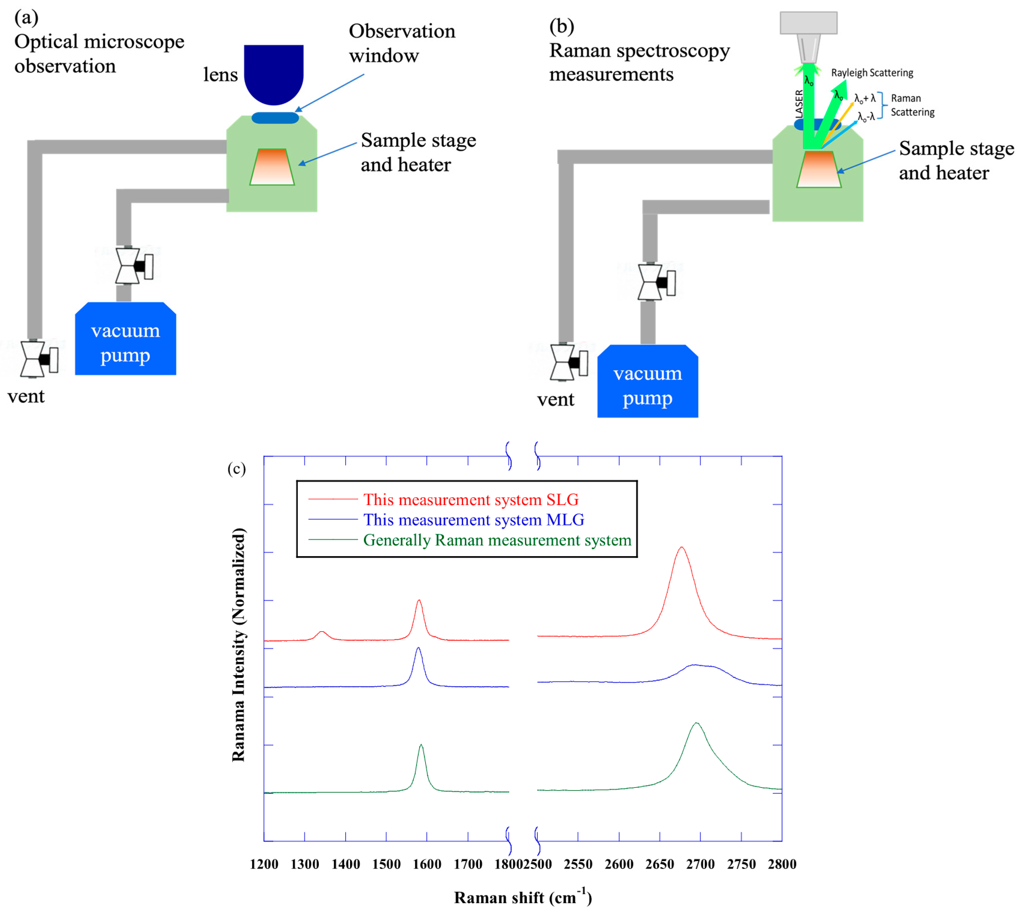
2. Experimental
2.1. CVD-Grown Graphene Films
2.2. Characterization Techniques
3. Results and Discussion
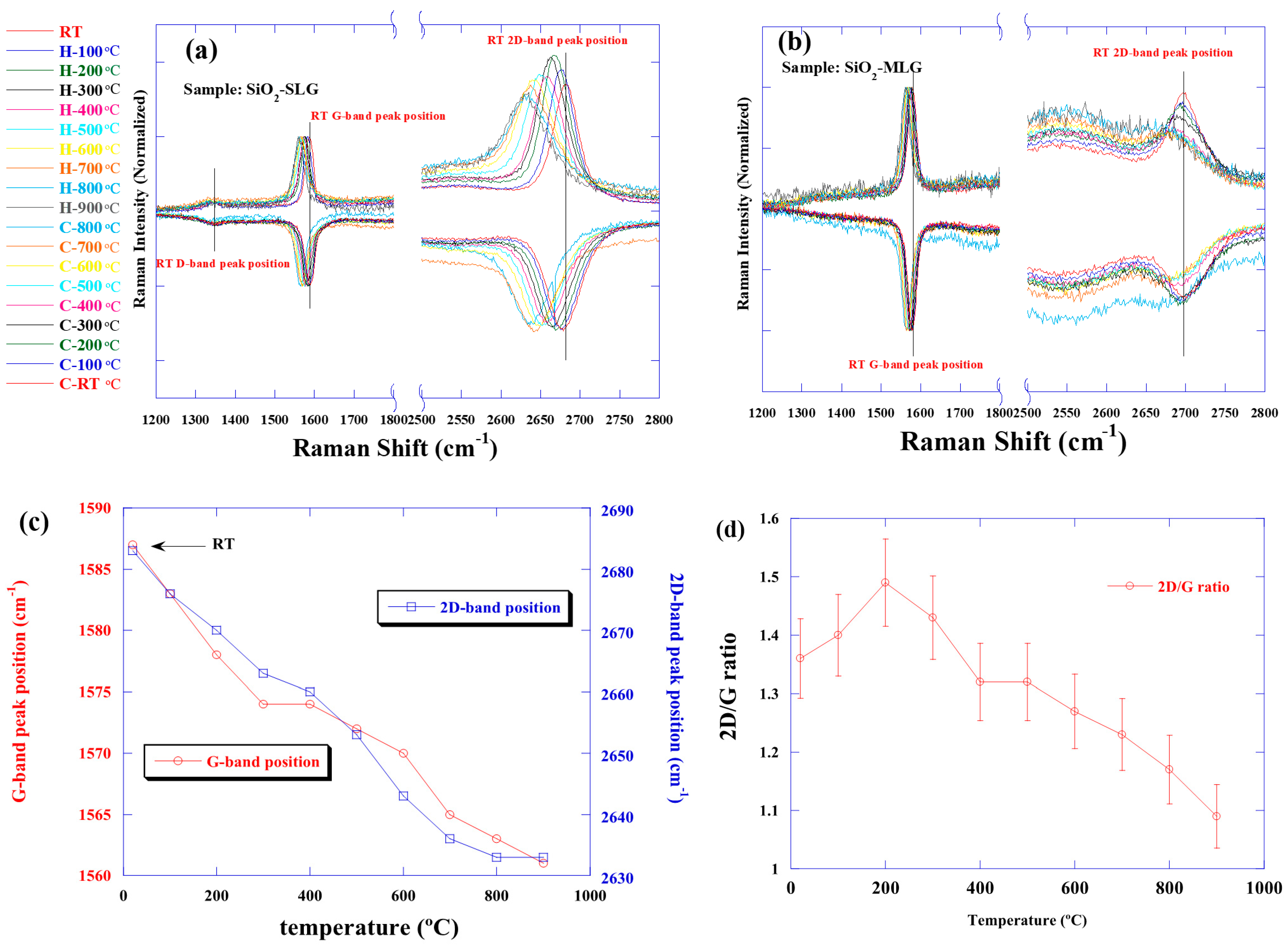
3.1. Raman Spectra of Transferred Graphene on SiO2 Substrate
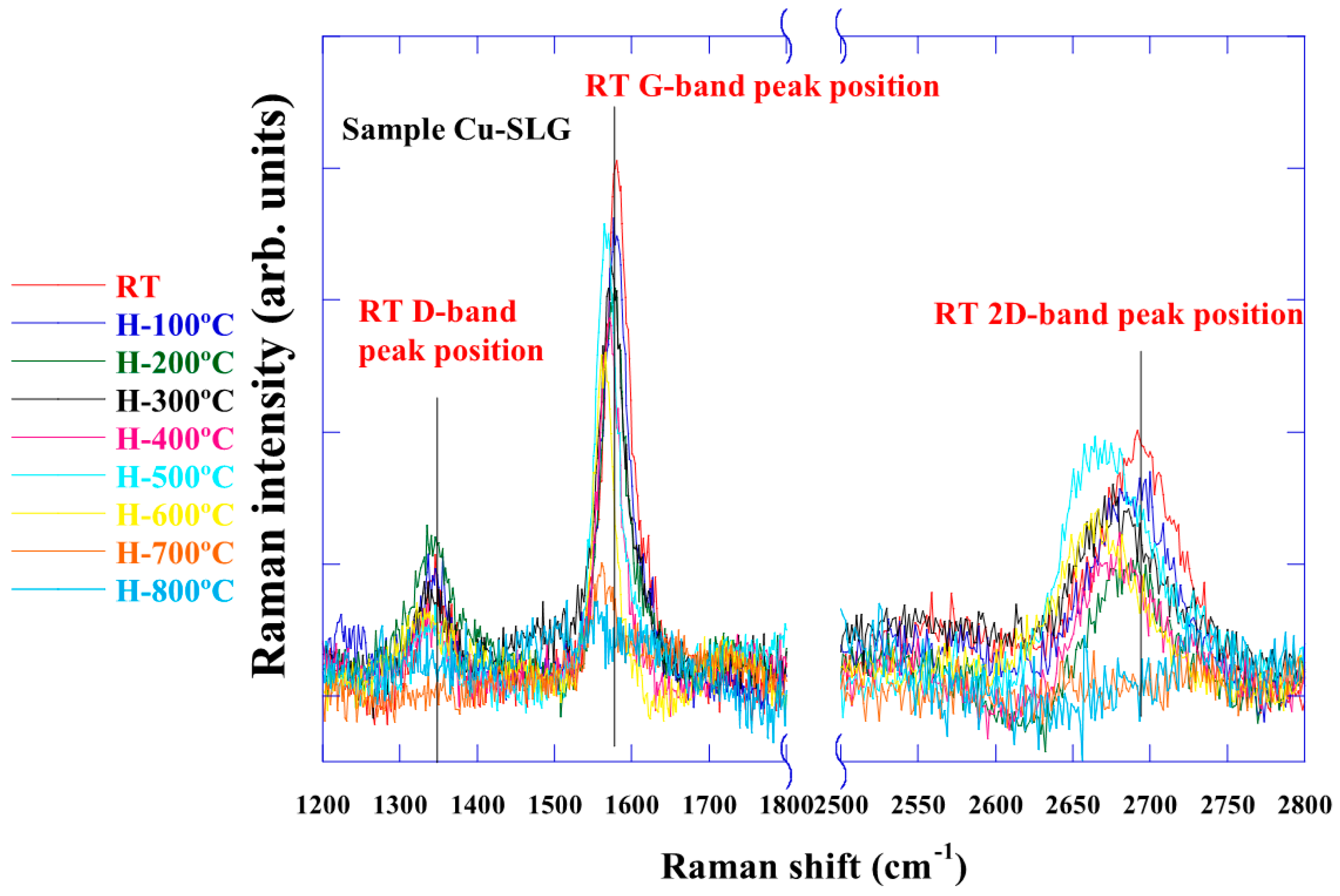
3.2. Raman Spectra of Graphene on Cu Foil
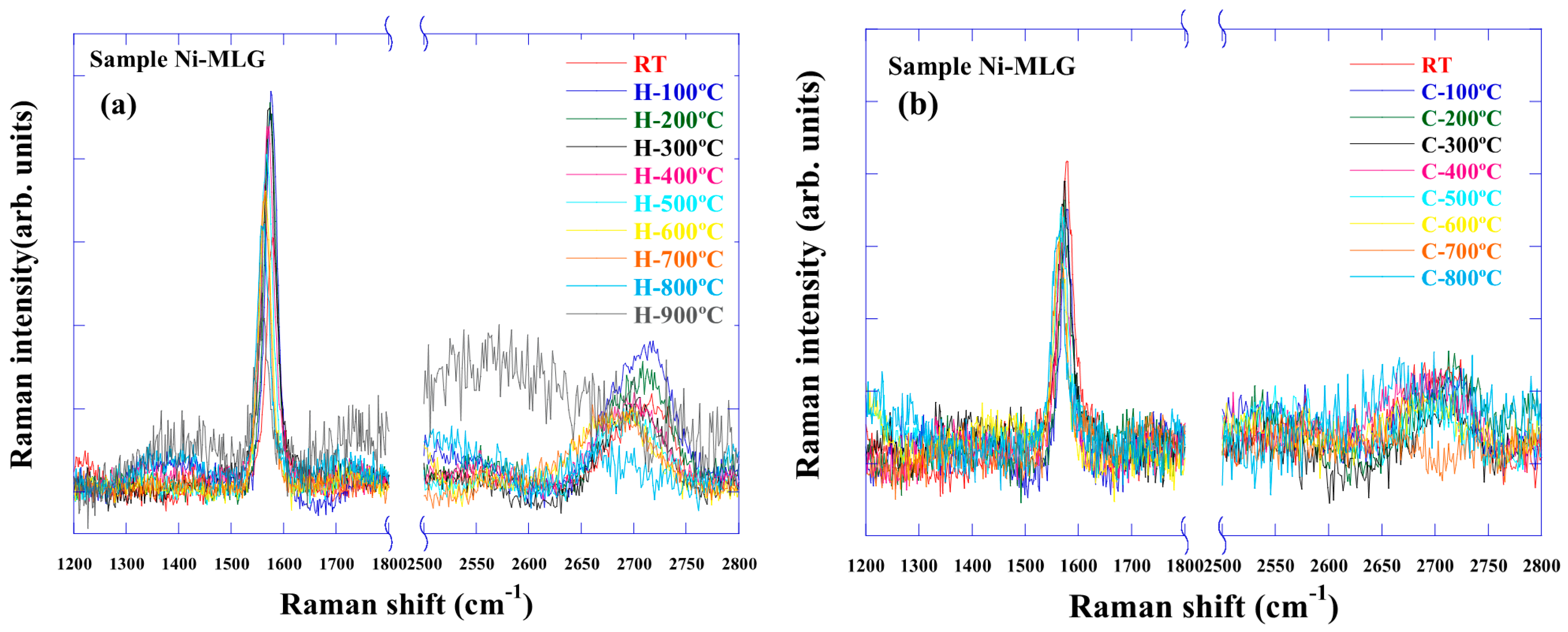
3.3. Raman Spectra of Graphene on Ni Foil
4. Conclusions
Author Contributions
Funding
Data Availability Statement
Conflicts of Interest
References
- Kwon, G.H.; Choi, B.; Young-Kook, L.; Moon, K. Influence of the Acetylene Flow Rate and Process Pressure on the Carbon Deposition Behavior by Thermal Chemical Vapor Deposition Process. Crystals 2024, 14, 782. [Google Scholar] [CrossRef]
- Tau, O.; Lovergine, N.; Prete, P. Adsorption and decomposition steps on Cu(111) of liquid aromatic hydrocarbon precursors for low-temperature CVD of graphene: A DFT study. Carbon 2023, 206, 142–149. [Google Scholar] [CrossRef]
- Bianco, G.V.; Losurdo, M.; Giangregorio, M.M.; Sacchetti, A.; Prete, P.; Lovergine, N.; Capezzuto, P.; Bruno, G. Direct epitaxial CVD synthesis of tungsten disulfide on epitaxial and CVD graphene. RSC Adv. 2015, 5, 98700–98708. [Google Scholar] [CrossRef]
- Ferrari, A.C.; Meyer, J.C.; Scardaci, V.; Casiraghi, C.; Lazzeri, M.; Mauri, F.; Piscanec, S.; Jiang, D.; Novoselov, K.S.; Roth, S.; et al. Raman spectrum of graphene and graphene layers. Phys. Rev. Lett. 2006, 97, 187401. [Google Scholar] [CrossRef] [PubMed]
- Calizo, I.; Balandin, A.A.; Bao, W.; Miao, F.; Lau, C.N. Temperature dependence of the Raman spectra of graphene and graphene multilayers. Nano Lett. 2007, 7, 2645–2649. [Google Scholar] [CrossRef]
- Ferrari, A.C. Raman spectroscopy of graphene and graphite: Disorder, electron–phonon coupling, doping and nonadiabatic effects. Solid State Commun. 2007, 143, 47–57. [Google Scholar] [CrossRef]
- Lee, J.E.; Ahn, G.; Shim, J.; Lee, Y.S.; Ryu, S. Optical separation of mechanical strain from charge doping in graphene. Nat. Commun. 2012, 3, 1024. [Google Scholar] [CrossRef] [PubMed]
- Ferrari, A.C.; Basko, D.M. Raman spectroscopy as a versatile tool for studying the properties of graphene. Nat. Nanotechnol. 2013, 8, 235–246. [Google Scholar] [CrossRef] [PubMed]
- Bruna, M.; Borini, S. Optical constants of graphene layers in the visible range. Appl. Phys. Lett. 2009, 94, 031901. [Google Scholar] [CrossRef]
- Roddaro, S.; Pingue, P.; Piazza, V.; Pellegrini, V.; Beltram, F. The optical visibility of graphene: Interference colors of ultrathin graphite on SiO2. Nano Lett. 2007, 7, 2707–2710. [Google Scholar] [CrossRef] [PubMed]
- Ogawa, Y.; Tawara, T.; Taniyasu, Y. In Situ Observation of Graphene Growth by Chemical Vapor Deposition Using Ultraviolet Reflection: Implications for Efficient Growth Control in the Industrial Process. ACS Appl. Nano Mater. 2023, 6, 21405–21411. [Google Scholar] [CrossRef]
- Lin, J.; Guo, L.; Huang, Q.; Jia, Y.; Li, K.; Lai, X.; Chen, X. Anharmonic phonon effects in Raman spectra of unsupported vertical graphene sheets. Phys. Rev. B 2011, 83, 125430. [Google Scholar] [CrossRef]
- Dresselhaus, M.S.; Dresselhaus, G.; Hofmann, M. Raman spectroscopy as a probe of graphene and carbon nanotubes. Philos. Trans. R. Soc. A Math. Phys. Eng. Sci. 2008, 366, 231–236. [Google Scholar] [CrossRef]
- Thomsen, C.; Reich, S. Double resonant Raman scattering in graphite. Phys. Rev. Lett. 2000, 85, 5214. [Google Scholar] [CrossRef] [PubMed]
- Saito, R.; Grüneis, A.; Samsonidze, G.G.; Brar, V.W.; Dresselhaus, G.; Dresselhaus, M.S.; Jorio, A.; Cançado, L.G.; Fantini, C.; Pimenta, M.A.; et al. Double resonance Raman spectroscopy of single-wall carbon nanotubes. New J. Phys. 2003, 5, 157. [Google Scholar] [CrossRef]
- Kamada, M.; Sasaki, K.I.; Matsui, T. Comprehensive study of optical contrast, reflectance, and Raman spectroscopy of multilayer graphene. Carbon Trends 2024, 16, 100389. [Google Scholar] [CrossRef]
- Cho, J.; Gao, L.; Tian, J.; Cao, H.; Wu, W.; Yu, Q.; Yitamben, E.N.; Fisher, B.; Guest, J.R.; Chen, Y.P.; et al. Atomic-scale investigation of graphene grown on Cu foil and the effects of thermal annealing. ACS Nano 2011, 5, 3607–3613. [Google Scholar] [CrossRef] [PubMed]
- Ni, Z.H.; Wang, H.M.; Luo, Z.Q.; Wang, Y.Y.; Yu, T.; Wu, Y.H.; Shen, Z.X. The effect of vacuum annealing on graphene. J. Raman Spectrosc. 2010, 41, 479–483. [Google Scholar] [CrossRef]
- Kato, M.; Guan, S.; Zhao, X. In-Situ observation of graphene using an optical microscope. Appl. Surf. Sci. Adv. 2021, 6, 100138. [Google Scholar] [CrossRef]
- Dahal, A.; Batzill, M. Graphene–nickel interfaces: A review. Nanoscale 2014, 6, 2548–2562. [Google Scholar] [CrossRef] [PubMed]

Disclaimer/Publisher’s Note: The statements, opinions and data contained in all publications are solely those of the individual author(s) and contributor(s) and not of MDPI and/or the editor(s). MDPI and/or the editor(s) disclaim responsibility for any injury to people or property resulting from any ideas, methods, instructions or products referred to in the content. |
© 2025 by the authors. Licensee MDPI, Basel, Switzerland. This article is an open access article distributed under the terms and conditions of the Creative Commons Attribution (CC BY) license (https://creativecommons.org/licenses/by/4.0/).
Share and Cite
Kato, M.; Zhao, X. In Situ Observation of the Thermal Behavior of Graphene on Insulating and Metal Substrates. Nanomaterials 2025, 15, 557. https://doi.org/10.3390/nano15070557
Kato M, Zhao X. In Situ Observation of the Thermal Behavior of Graphene on Insulating and Metal Substrates. Nanomaterials. 2025; 15(7):557. https://doi.org/10.3390/nano15070557
Chicago/Turabian StyleKato, Mikihiro, and Xinwei Zhao. 2025. "In Situ Observation of the Thermal Behavior of Graphene on Insulating and Metal Substrates" Nanomaterials 15, no. 7: 557. https://doi.org/10.3390/nano15070557
APA StyleKato, M., & Zhao, X. (2025). In Situ Observation of the Thermal Behavior of Graphene on Insulating and Metal Substrates. Nanomaterials, 15(7), 557. https://doi.org/10.3390/nano15070557