
Optimal Selection and Experimental Verification of Wide-Bandgap Semiconductor for Betavoltaic Battery
 ,
,
Abstract
1. Introduction
2. Methods
2.1. Theoretical Model
2.1.1. Efficiency Calculation
2.1.2. Upper-Limit Efficiency
2.1.3. Energy Deposition Simulation
2.2. Experiment
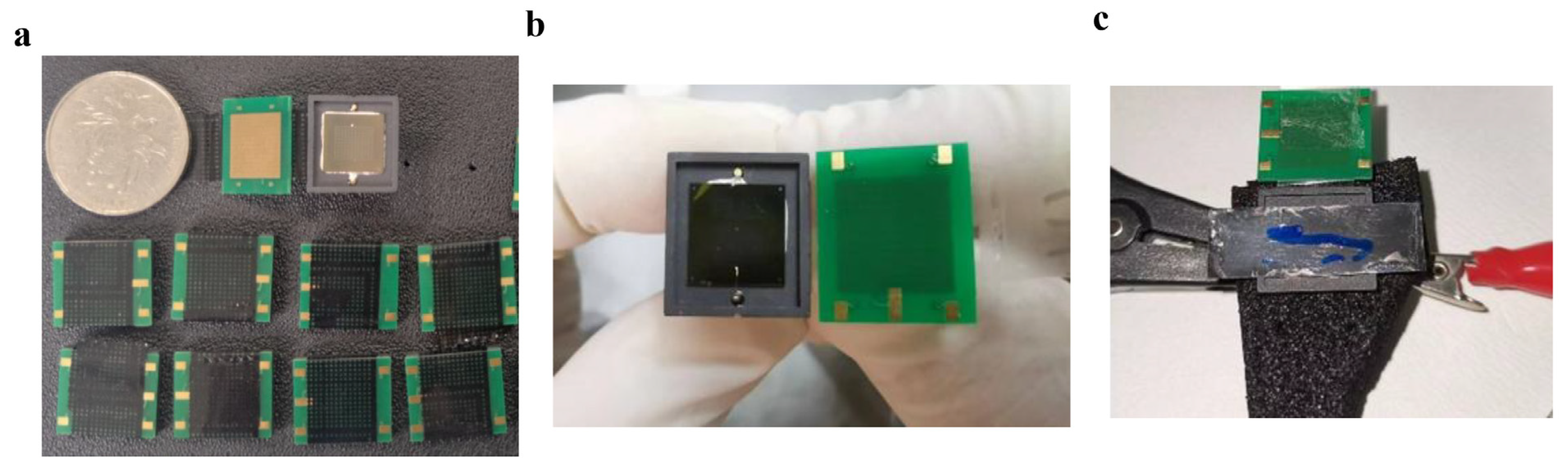
2.2.1. Fabrication
2.2.2. Measurement
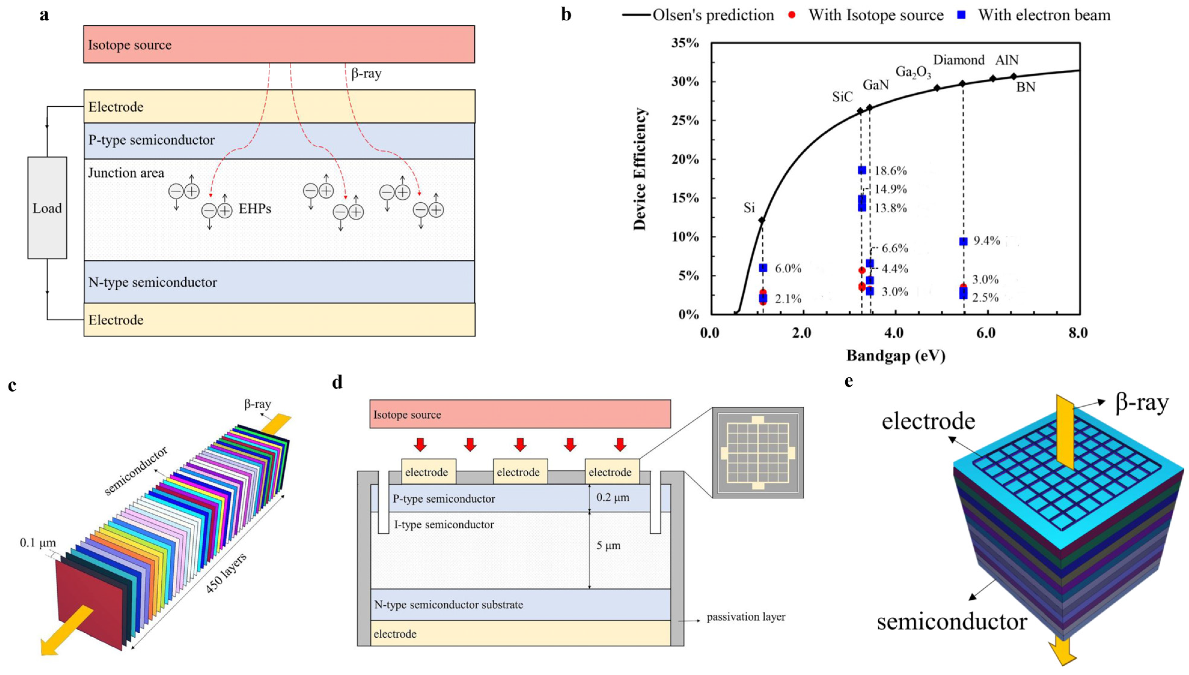
3. Results and Discussion
3.1. Selection of Typical Wide-Bandgap Semiconductor
3.1.1. Effect of the Electron–Hole Pair Creation Energy
3.1.2. Effect of the Energy Deposition of Beta Particles
3.1.3. Effect of the Electron–Hole Pairs Collection Efficiency
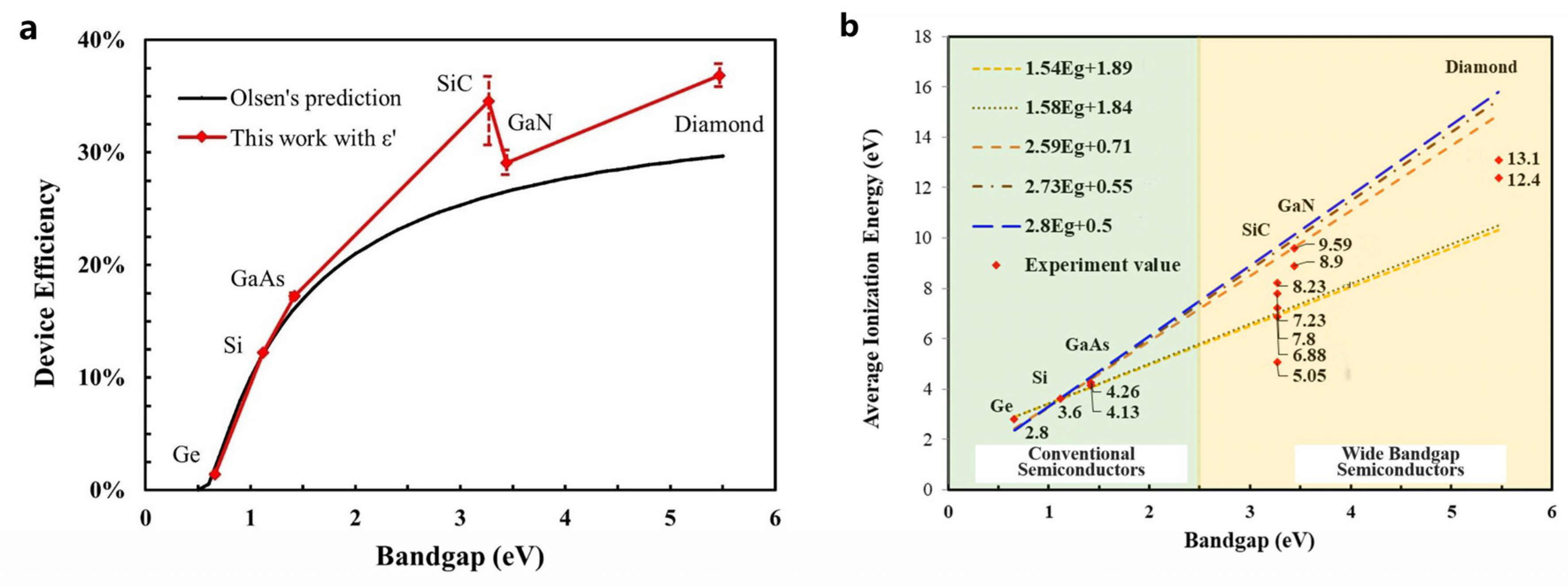
3.1.4. The Ideal Efficiency
3.2. Prediction of Ultra-Wide-Bandgap Semiconductor
3.3. Efficiency Prediction of the SiC Experimental Device
3.4. Measurement of the SiC Experimental Device
3.4.1. Measurement of Electron Beam
3.4.2. Measurement of 63Ni Source
4. Conclusions
Author Contributions
Funding
Data Availability Statement
Conflicts of Interest
References
- Zambelli, C.; Olivo, P.; Gaddi, R.; Schepens, C.; Smith, C. Characterization of a Mems-Based Embedded Non Volatile Memory Array for Extreme Environments. In Proceedings of the 3rd IEEE IMW, Monterey, CA, USA, 22–25 May 2011. [Google Scholar] [CrossRef]
- Nathan, M.; Peled, E.; Haronian, D. Micro Electrochemical Energy Storage Cells. United States Patent RE42273, 4 May 2011. Available online: https://www.freepatentsonline.com/6197450.html (accessed on 10 May 2022).
- Olsen, L.C. Review of Betavoltaic Energy Conversion. In Proceedings of the XII Space Photovoltaic Research and Technology Conference (SPRAT XII), Cleveland, OH, USA, 20–22 October 1992; Available online: https://ntrs.nasa.gov/citations/19940006935 (accessed on 15 May 2022).
- Theirrattanakul, S.; Prelas, M. A methodology for efficiency optimization of betavoltaic cell design using an isotropic planar source having an energy dependent beta particle distribution. Appl. Radiat. Isot. 2017, 127, 41–46. [Google Scholar] [CrossRef]
- Prelas, M.; Boraas, M.; Aguilar, F.D.; Seelig, J.-D.; Tchouaso, M.T.; Wisniewski, D. Nuclear Batteries and Radioisotopes; Springer: Cham, Switzerland, 2016. [Google Scholar] [CrossRef]
- Zhao, C.; Liu, A.; Bai, S.; Zhao, Y. Understanding Efficiency Differences of Betavoltaic Batteries Measured by Electron Gun Mimicked Source and Radioactive β Source. Appl. Phys. Lett. 2020, 117, 193901. [Google Scholar] [CrossRef]
- Grzanka, S.; Marona, L.; Winiewski, P.; Targowski, G.; Zaręba, B.; Wincel, K.; Klimasz, M.; Jacek, T.L.; Laskowski, K.P.; Kacperski, J.; et al. Highly Stable GaN-Based Betavoltaic Structures Grown on Different Dislocation Density Substrates. Solid-State Electron. 2020, 167, 107784. [Google Scholar] [CrossRef]
- Delfaure, C.; Pomorski, M.; Sanoit, J.D.; Bergonzo, P.; Saada, S. Single Crystal CVD Diamond Membranes for Betavoltaic Cells. Appl. Phys. Lett. 2016, 108, 246–247. [Google Scholar] [CrossRef]
- Heuser, T.; Braun, M.; McIntyre, P.; Senesky, D.G. Electron Beam Irradiation of Gallium Nitride-On-Silicon Betavoltaics Fabricated with a Triple Mesa Etch. J. Appl. Phys. 2021, 130, 174503. [Google Scholar] [CrossRef]
- Zhao, C.; Lei, L.; Liao, F.; Yuan, D.; Zhao, Y. Efficiency Prediction of Planar Betavoltaic Batteries Basing on Precise Modeling of Semiconductor Units. Appl. Phys. Lett. 2020, 117, 263901. [Google Scholar] [CrossRef]
- Thomas, C.; Portnoff, S.; Spencer, M.G. High Efficiency 4H-SiC Betavoltaic Power Sources Using Tritium Radioisotopes. Appl. Phys. Lett. 2016, 108, 8037–8058. [Google Scholar] [CrossRef]
- Bao, R.; Brand, P.J.; Chrisey, D.B. Betavoltaic Performance of Radiation-Hardened High-Efficiency Si Space Solar Cells. IEEE Trans. Electron Dev. 2012, 59, 1286–1294. [Google Scholar] [CrossRef]
- Khan, M.R.; Smith, J.R.; Tompkins, R.P.; Kelley, S.; Litz, M.; Russo, J.; Leathersich, J.; Shahedipour-Sandvik, F.; Jones, K.A.; Iliadis, A. Design and Characterization of GaN P-I-N Diodes for Betavoltaic Devices. Solid-State Electron. 2017, 136, 24–29. [Google Scholar] [CrossRef]
- Grushko, V.; Beliuskina, O.; Mamalis, A.; Lysakovskiy, V.; Mitskevich, E.; Kiriev, A.; Petrosyan, E.; Chaplynskyi, R.; Bezshyyko, O.; Lysenko, O. Energy conversion efficiency in betavoltaic cells based on the diamond Schottky diode with a thin drift layer. Appl. Radiat. Isot. 2020, 157, 109017. [Google Scholar] [CrossRef]
- Bormashov, V.S.; Troschiev, S.Y.; Tarelkin, S.A.; Volkov, A.P.; Teteruk, D.V.; Golovanov, A.V.; Kuznetsov, M.S.; Kornilov, N.V.; Terentiev, S.A.; Blank, V.D. High Power Density Nuclear Battery Prototype Based on Diamond Schottky Diodes. Diam. Relat.Mater. 2018, 84, 41–47. [Google Scholar] [CrossRef]
- Ishibe, T.; Tomeda, A.; Komatsubara, Y.; Kitaura, R.; Uenuma, M.; Uraoka, Y.; Yamashita, Y.; Nakamura, Y. Carrier and phonon transport control by domain engineering for high-performance transparent thin film thermoelectric generator. J. Appl. Phys. Lett. 2021, 118, 151601. [Google Scholar] [CrossRef]
- Li, F.; Zhang, S.; Xu, Z.; Wei, X.; Shrout, T.R. Critical Property in Relaxor-PbTiO (3) Single Crystals—Shear Piezoelectric Response. J. Adv. Funct. Mater. 2011, 21, 2118–2128. [Google Scholar] [CrossRef] [PubMed]
- Liao, M.; Shen, B.; Wang, Z. Ultra-Wide Bandgap Semiconductor Materials; Elsevier: Amsterdam, The Netherlands, 2019. [Google Scholar] [CrossRef]
- Tang, X.; Ding, D.; Liu, Y.; Chen, D. Optimization design and analysis of Si-63Ni betavoltaic battery. Sci. China Technol. Sci. 2012, 55, 990–996. [Google Scholar] [CrossRef]
- Chandrashekhar, M.; Thomas, C.I.; Spencer, M.G. Measurement of the Mean Electron-Hole Pair Ionization Energy in 4H-SiC. Appl. Phys. Lett. 2006, 89, 042113. [Google Scholar] [CrossRef]
- Honsberg, C.; Doolittle, W.A.; Allen, M.; Wang, C. GaN Betavoltaic Energy Converters. In Proceedings of the Thirty-First IEEE Photovoltaic Specialists Conference, Lake Buena Vista, FL, USA, 3–7 January 2005. [Google Scholar] [CrossRef]
- Anderson, B. Fundamentals of Semiconductor Devices; McGraw-Hill Higher Education: New York, NY, USA, 2006. [Google Scholar]
- Ye, Z. Determination of Average Energy Consumption by Electron-Hole Generation in Silicon by α Particles Atomic Energy. Sci. Technol. 1977, 11, 273. (In Chinese) [Google Scholar]
- Song, Z.; Zhao, C.; Liao, F.; Zhao, Y. Perovskite-Betavoltaic Cells: A Novel Application of Organic-Inorganic Hybrid Halide Perovskites. ACS Appl. Mater. Interfaces 2019, 11, 32969–32977. [Google Scholar] [CrossRef]
- Lioliou, G.; Barnett, A.M. Electron-hole pair creation and conversion efficiency in radioisotope microbatteries. Appl. Radiat. Isot. 2022, 180, 110042. [Google Scholar] [CrossRef]
- Butera, S.; Lioliou, G.; Krysa, A.B.; Barnett, A.M. Measurement of the Electron–Hole Pair Creation Energy in Al0.52in0.48P Using X-Ray Radiation. Nucl. Instrum. Methods Phys. Res. 2018, 879, 64–68. [Google Scholar] [CrossRef]
- Kobayashi, T. Average Energy to Form Electron-Hole Pairs in Gap Diodes with Alpha Particles. Appl. Phys. Lett. 1972, 21, 150–152. [Google Scholar] [CrossRef]
- Bloom, S.; Alig, R.C. Electron-Hole-Pair Creation Energies in Semiconductors. Phys. Rev. Lett. 1975, 35, 1522–1525. [Google Scholar] [CrossRef]
- Chaudhuri, S.K.; Zavalla, K.J.; Mandal, K.C. Experimental Determination of Electron-Hole Pair Creation Energy in 4H-SiC Epitaxial Layer: An Absolute Calibration Approach. Appl. Phys. Lett. 2013, 102, 031109. [Google Scholar] [CrossRef]
- Bertuccio, G.; Maiocchi, D. Electron-Hole Pair Generation Energy in Gallium Arsenide by X. and Γ Photons. J. Appl. Phys. 2002, 92, 1248–1255. [Google Scholar] [CrossRef]
- Lo Giudice, A.; Fizzotti, F.; Manfredotti, C.; Vittone, E.; Nava, F. Average Energy Dissipated by Mega-Electron-Volt Hydrogen and Helium Ions Per Electron-Hole Pair Generation in 4H-SiC. Appl. Phys. Lett. 2005, 87, 222105. [Google Scholar] [CrossRef]
- Yong, J.; Fan, X.; Rong, R.; Wu, J.; Bai, S.; Li, L. Properties Measurement of Silicon Carbide Detector. Nucl. Electron. Detect. Technol. 2012, 32, 1372–1375+1427. [Google Scholar]
- Wrbanek, J.; Wrbanek, S.; Fralick, G. Micro-Fabricated Solid-State Radiation Detectors for Active Personal Dosimetry. 2007. Available online: https://ntrs.nasa.gov/citations/20070014753 (accessed on 20 May 2022).
- Nava, F.; Bertuccio, G.; Cavallini, A.; Vittone, E. Silicon Carbide and its Use as a Radiation Detector Material. Meas. Sci. Technol. 2008, 19, 102001. [Google Scholar] [CrossRef]
- Krasnov, A.A.; Legotin, S.A. Advances in the Development of Betavoltaic Power Sources (a Review). Instrum. Exp. Tech. 2020, 63, 437–452. [Google Scholar] [CrossRef]
- Yakimov, E.B.; Polyakov, A.Y.; Shchemerov, I.V.; Smirnov, N.B.; Vasilev, A.A.; Vergeles, P.S.; Yakimov, E.E.; Chernykh, A.V.; Ren, F.; Pearton, S.J. Experimental Estimation of Electron-Hole Pair Creation Energy in β-Ga2O3. Appl. Phys. Lett. 2021, 118, 202106. [Google Scholar] [CrossRef]
- Pivrikas, A. Charge Transport Characteristics in Doped Organic Semiconductors Using Hall Effect. J. Electron. 2024, 13, 4223. [Google Scholar] [CrossRef]
- Morab, S.; Sundaram, M.M.; Pivrikas, A. Review on Charge Carrier Transport in Inorganic and Organic Semiconductors. Coatings 2023, 13, 1657. [Google Scholar] [CrossRef]
- Neamen, D.A. Semiconductor Physics and Devices; McGraw-Hill Higher Education: New York, NY, USA, 2011. [Google Scholar]
- Zhou, M.; Li, Z.; Fan, S.; Xu, Z.; Xiong, Z. Progress of the Growth of GaN Single Crystals. China Light. Light. 2017, 9, 8–17. [Google Scholar] [CrossRef]
- Wang, L.; Wang, F.; Liu, F.; Wang, J.; Lu, Z. Review of Diamond Semiconductor Devices. J. Wuhan Inst. Technol. 2020, 42, 518–525. [Google Scholar] [CrossRef]
- Dutta, M.; Koeck, F.; Hathwar, R.; Goodnick, S.M.; Nemanich, R.J.; Chowdhury, S. Demonstration of Diamond-Based Schottky P-I-N Diode with Blocking Voltage > 500 V. IEEE Electron Device Lett. 2016, 37, 1170–1173. [Google Scholar] [CrossRef]
- Liu, Z.; Zhao, D. Fabrication and Characterization of (100)-Oriented Single Crystal Diamond P-I-N Junction Ultraviolet Detector. Phys. Status Solidi. A Appl. Mater. Sci. 2020, 217, 2000207. [Google Scholar] [CrossRef]
- Maity, A.; Doan, T.C.; Li, J.; Lin, J.Y.; Jiang, H.X. Realization of Highly Efficient Hexagonal Boron Nitride Neutron Detectors. Appl. Phys. Lett. 2016, 109, 072101. [Google Scholar] [CrossRef]
- Tsao, J.Y.; Chowdhury, S.; Hollis, M.A.; Jena, D.; Johnson, N.M.; Jones, K.A.; Kaplar, R.J.; Rajan, S.; Van de Walle, C.G.; Bellotti, E.; et al. Ultrawide-Bandgap Semiconductors: Research Opportunities and Challenges. Adv. Electron. Mater. 2018, 4, 1600501. [Google Scholar] [CrossRef]
- Zhang, C.; Liao, F.; Liang, X.; Gong, H.; Liu, Q.; Li, L.; Qin, X.; Huang, X.; Huang, C. Electronic Transport Properties in Metal Doped Beta-Ga2O3: A First Principles Study. Phys. B 2019, 562, 124–130. [Google Scholar] [CrossRef]
- Lopatiuk-Tirpak, O.; Chernyak, L.; Borisov, B.A.; Kuryatkov, V.V.; Nikishin, S.A.; Gartsman, K. Electron Irradiation-Induced Increase of Minority Carrier Diffusion Length, Mobility, and Lifetime in Mg-doped AlN/AlGaN Short Period Superlattice. Appl. Phys. Lett. 2007, 91, 182103. [Google Scholar] [CrossRef]
- Cao, B.; Tian, Y.; Wen, H.F.; Guo, H.; Wu, X.; Li, L.; Zhang, Z.; Liu, L.; Zhu, Q.; Tang, J.; et al. Recent progress on fabrication, spectroscopy properties, and device applications in Sn-doped CdS micro-nano structures. J. Semicond. 2024, 45, 091101. [Google Scholar]
- Gao, P.; Li, X.-Y.; Yao, X.W. 4H-SiC Schottky Betavoltaic Micro Battery. Micronanoelectron. Technol. 2010, 47, 157–162. [Google Scholar]
- Chandrasekhar, M.; Thomas, C.I.; Li, H.; Spencer, M.G.; Lal, A. Demonstration of a 4H-SiC Betavoltaic Cell. Appl. Phys. Lett. 2006, 88, 33506. [Google Scholar] [CrossRef]
- Lu, M.; Wang, G.; Yao, C.S. Gallium Nitride for Nuclear Batteries. Adv. Mater. Res. 2012, 343–344, 56–61. [Google Scholar] [CrossRef]
- Cheng, Z.-J.; San, H.-S.; Chen, X.-Y.; Liu, B.; Feng, Z.-H. Demonstration of a High Open-Circuit Voltage GaN Betavoltaic Microbattery. Chin. Phys. Lett. 2011, 28, 78401. [Google Scholar] [CrossRef]


| Semiconductor | SiC | GaN | Diamond | Ga2O3 | AlN | BN |
|---|---|---|---|---|---|---|
| Jsc/nA·cm−2 | 110.16 | 95.18 | 72.18 | 51.18 | 43.62 | 64.67 |
| Voc/V | 2.24 | 2.40 | 4.39 | 3.81 | 5.31 | 5.75 |
| ηd | 22.17% | 20.69% | 29.29% | 17.98% | 21.57% | 34.65% |
| Semiconductor | Ga2O3 | AlN | BN |
|---|---|---|---|
| Bandgap/eV | 4.9 | 6.13 | 6.4 |
| Density/g·cm−3 | 6.1 | 3.26 | 3.49 |
| Electron–hole pair creation energy/eV | 15.6 | 14.4 * | 15.0 * |
| Relative dielectric constant | 10 | 8.6 | 7.1 |
| Intrinsic carrier concentration/cm−3 | 2.81 × 10⁻²³ | 3.82 × 10−36 | 8.83 × 10−39 |
| Minority carrier diffusion length/μm | 0.325 | 0.15 | 7.6 |
| Carrier mobility/cm2·V−1yggs−1 | 20 | 14 | 500 |
| Bandgap type | direct | direct | indirect |
| Source | Condition | Isc/nA | Voc/V | FF | ηd | n |
|---|---|---|---|---|---|---|
| Electron beam | original prediction | 197.71 | 2.25 | 0.94 | 23.17% | 1 |
| prediction with experimental n | 197.71 | 1.66 | 0.92 | 16.32% | 1.36 | |
| measurement | 195.28 | 1.54 | 0.89 | 14.88% | 1.36 | |
| 63Ni | original prediction | 2.99 | 1.89 | 0.91 | 17.54% | 1 |
| prediction with experimental I0 | 2.99 | 1.42 | 0.88 | 12.83% | 1.51 | |
| measurement | 2.91 | 1.41 | 0.81 | 7.31% | 1.51 |
Disclaimer/Publisher’s Note: The statements, opinions and data contained in all publications are solely those of the individual author(s) and contributor(s) and not of MDPI and/or the editor(s). MDPI and/or the editor(s) disclaim responsibility for any injury to people or property resulting from any ideas, methods, instructions or products referred to in the content. |
© 2025 by the authors. Licensee MDPI, Basel, Switzerland. This article is an open access article distributed under the terms and conditions of the Creative Commons Attribution (CC BY) license (https://creativecommons.org/licenses/by/4.0/).
Share and Cite
Zhang, J.; Lv, K.; Yin, Y.; Gao, Y.; Tian, Y.; Han, Y.; Tang, J. Optimal Selection and Experimental Verification of Wide-Bandgap Semiconductor for Betavoltaic Battery. Nanomaterials 2025, 15, 635. https://doi.org/10.3390/nano15090635
Zhang J, Lv K, Yin Y, Gao Y, Tian Y, Han Y, Tang J. Optimal Selection and Experimental Verification of Wide-Bandgap Semiconductor for Betavoltaic Battery. Nanomaterials. 2025; 15(9):635. https://doi.org/10.3390/nano15090635
Chicago/Turabian StyleZhang, Jiachen, Kunlun Lv, Yuan Yin, Yuqian Gao, Ye Tian, Yuncheng Han, and Jun Tang. 2025. "Optimal Selection and Experimental Verification of Wide-Bandgap Semiconductor for Betavoltaic Battery" Nanomaterials 15, no. 9: 635. https://doi.org/10.3390/nano15090635
APA StyleZhang, J., Lv, K., Yin, Y., Gao, Y., Tian, Y., Han, Y., & Tang, J. (2025). Optimal Selection and Experimental Verification of Wide-Bandgap Semiconductor for Betavoltaic Battery. Nanomaterials, 15(9), 635. https://doi.org/10.3390/nano15090635