Article

SnO Nanosheet Transistor with Remarkably High Hole Effective Mobility and More than Six Orders of Magnitude On-Current/Off-Current

by
Kuan-Chieh Chen
,
Jiancheng Wu
,
Pheiroijam Pooja
and
Albert Chin
*
Department of Electronics Engineering, National Yang Ming Chiao Tung University, Hsinchu 300, Taiwan
*
Author to whom correspondence should be addressed.
Nanomaterials 2025, 15(9), 640; https://doi.org/10.3390/nano15090640
Submission received: 24 March 2025 / Revised: 18 April 2025 / Accepted: 22 April 2025 / Published: 23 April 2025
(This article belongs to the Special Issue Integrated Circuit Research for Nanoscale Field-Effect Transistors)

Abstract

:
Using novel SiO2 surface passivation and ultraviolet (UV) light anneal, a 12 nm thick SnO p-type FET (pFET) shows hole effective mobilities (µeff) of more than 100 cm2/V·s and 31.1 cm2/V·s at hole densities (Qh) of 1 × 10¹¹ and 5 × 1012 cm−2, respectively. To further improve the on-current/off-current (ION/IOFF), an ultra-thin 7 nm thick SnO nanosheet pFET shows a record-breaking ION/IOFF of 6.9 × 10⁶ and remarkable µeff values of ~70 cm2/V·s and 20.7 cm2/V·s at Qh of 1 × 1011 cm−2 and 5 × 1012 cm−2, respectively. This is the first report of an oxide semiconductor transistor achieving a hole effective mobility µeff that reaches 20% of that in single-crystal Si pFETs at an ultra-thin body thickness of 7 nm. In sharp contrast, the control SnO nanosheet pFET without surface passivation or UV anneal exhibits a small ION/IOFF of 1.8 × 10⁴ and a µeff of only 6.1 cm2/V·s at 5 × 1012 cm−2 Qh. The enhanced SnO pFET performance is attributed to reduced defects and improved quality in the SnO channel, as confirmed by decreased charges related to sub-threshold swing (SS) and threshold voltage (Vth) shift. Such a large improvement is further supported by the increased Sn2+ after passivation and UV anneal, as evidenced by X-ray photoelectron spectroscopy (XPS) analysis. The ION/IOFF ratio exceeding six orders of magnitude, remarkably high hole µeff, and excellent two-month stability demonstrate that this pFET is a strong candidate for integration with SnON nFETs in next-generation ultra-high-definition displays and monolithic three-dimensional integrated circuits (3D ICs).

1. Introduction

Oxide semiconductors possess unique carrier transport characteristics [1]. The SnO2 n-type field-effect transistor (nFET) has achieved a superb high field-effect mobility (µFE) [2] close to the single-crystal Si nanosheet nFET and phonon-scattering-limited two-dimensional (2D) MoS2 nFETs [3,4]. However, p-type FETs (pFETs) are indispensable in forming low-DC-power Complementary Metal–Oxide–Semiconductor (CMOS) logic integrated circuits (ICs). The development of p-channel oxide TFTs remains challenging, as hole transport is highly sensitive to film quality and can be easily degraded by structural defects [5]. Materials such as tin monoxide (SnO), copper oxide (Cu2O), and nickel oxide (NiO) have emerged as promising p-type channel candidates due to their intrinsic hole conduction properties and compatibility with low-temperature processing. Recent advancements have focused on enhancing hole mobility through interface engineering, bilayer structures, and the incorporation of high-κ dielectrics. In particular, SnO-based pFETs have demonstrated notable improvements in hole mobility and thermal stability, enabled by advanced deposition techniques and optimized interface quality. For example, low-temperature processing has facilitated the integration of SnO pFETs into flexible electronic platforms [6]. Che et al. obtained a µFE of 6.13–7.24 cm2/V·s without using high-temperature post-anneal and improved sub-threshold swing characteristics by reducing surface defect states using backchannel passivation with an Al2O3 film [7]. Cu2O has also attracted interest for its inherent p-type conductivity and suitability for transparent electronics. Innovations in deposition techniques, such as aerosol-assisted chemical vapor deposition (AACVD), have enabled the fabrication of high-quality Cu2O thin films [8]. NiO, known for its wide bandgap and chemical stability, has been explored as another viable p-type semiconductor. Liu et al. reported a remarkable 60-fold enhancement in hole mobility from 0.07 to 4.4 cm2/V·s, primarily attributed to the high areal capacitance of the Al2O3 dielectric and the high-quality NiOx/Al2O3 interface, compared to conventional SiO2-based dielectrics [9]. Among the various oxide semiconductors, SnO has garnered significant attention due to its small hole effective mass [10,11,12,13,14,15,16], which originates from the strong orbital overlap between Sn 5s and O 2p states near the valence band edge [13,14]. Nevertheless, the development of high-performance SnO pFETs is hindered by oxide defects and the co-existence of n-type SnO2−x [13]. In addition, SnO faces practical challenges such as sensitivity to moisture, stoichiometry control, and unavoidable oxygen vacancies, which may form nonstoichiometric phases such as Sn2O3 or Sn3O4 [15].
In this work, the record-breaking performance of an oxide-semiconductor pFET is reported, where the SnO pFET achieves a record-breaking on-current/off-current (ION/IOFF) of 6.9 × 10⁶. Such a high ION/IOFF is mandatory for low-DC-power ICs. Furthermore, the device exhibits remarkably high effective mobilities (µeff) of ~70 cm2/V·s and 20.7 cm2/V·s at hole densities (Qh) of 1 × 1011 cm−2 and 5 × 1012 cm−2, respectively. This record high performance among oxide semiconductor pFETs is attributed to the successful passivation of SnO surface defects and ultraviolet (UV) light anneal [16,17]. The passivation layer not only protects the SnO channel from moisture degradation, but also minimizes defect states, resulting in improved carrier transport. This excellent SnO pFET can be further integrated with the record-high-mobility SnON nFET [2] on the back end of ICs, forming low-DC-power CMOS logic ICs and being useful for monolithic three-dimensional (M3D) ICs.

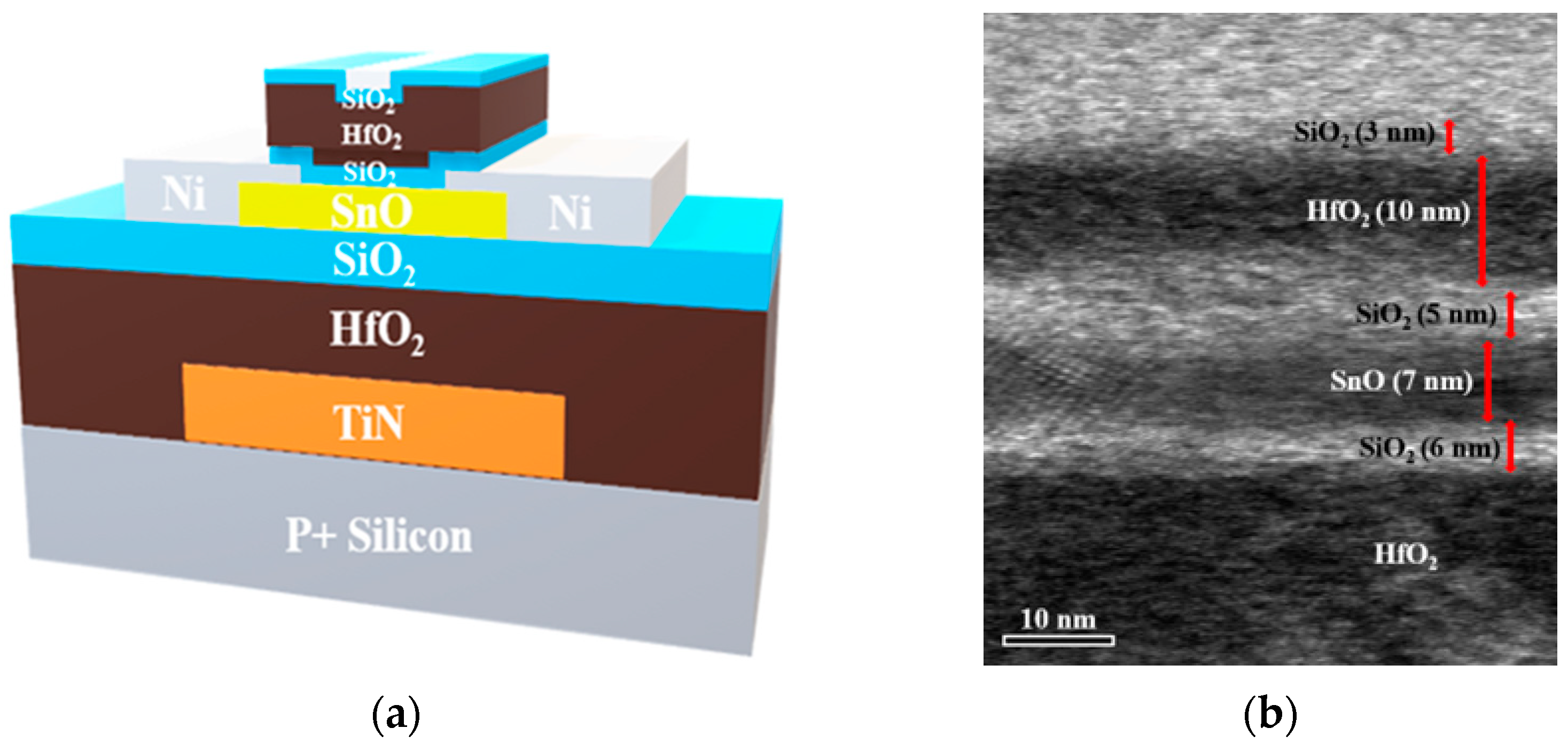
2. Materials and Methods
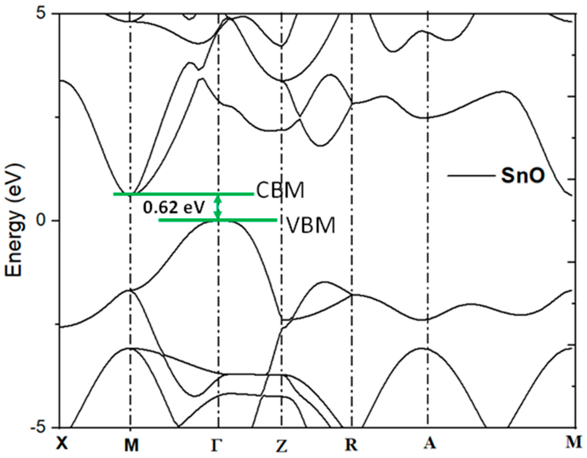
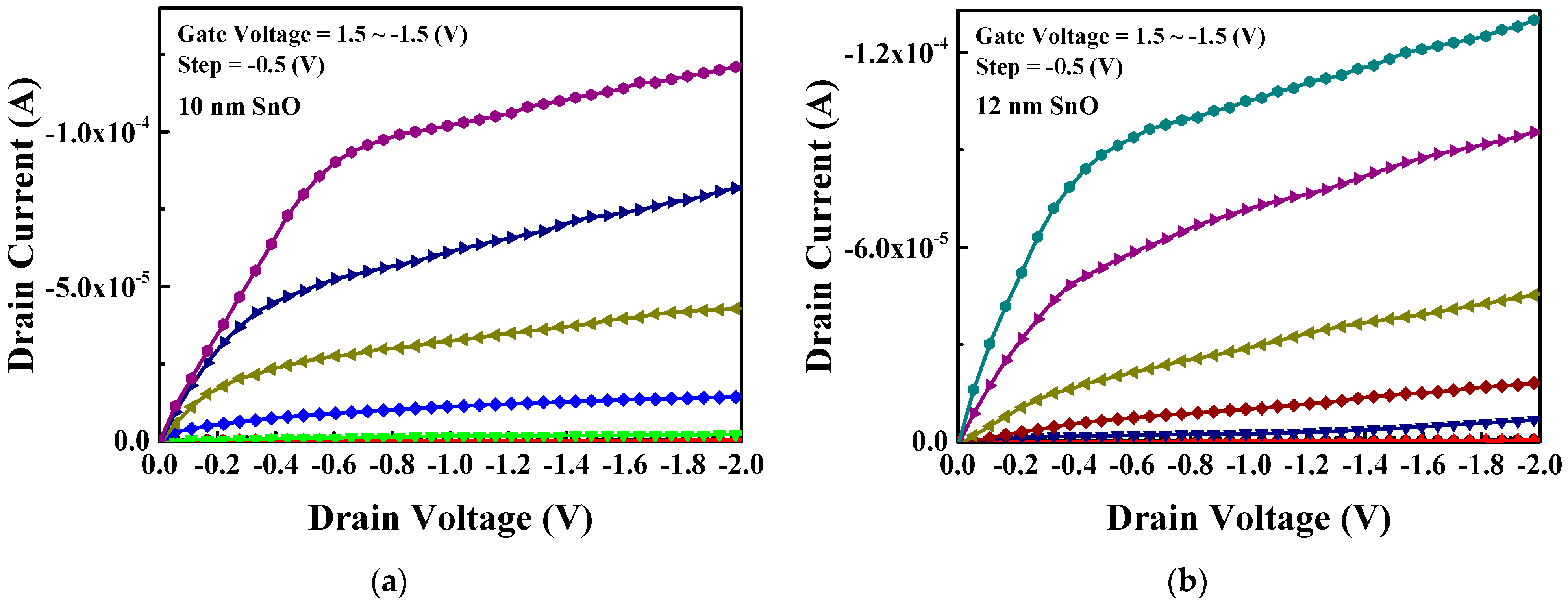
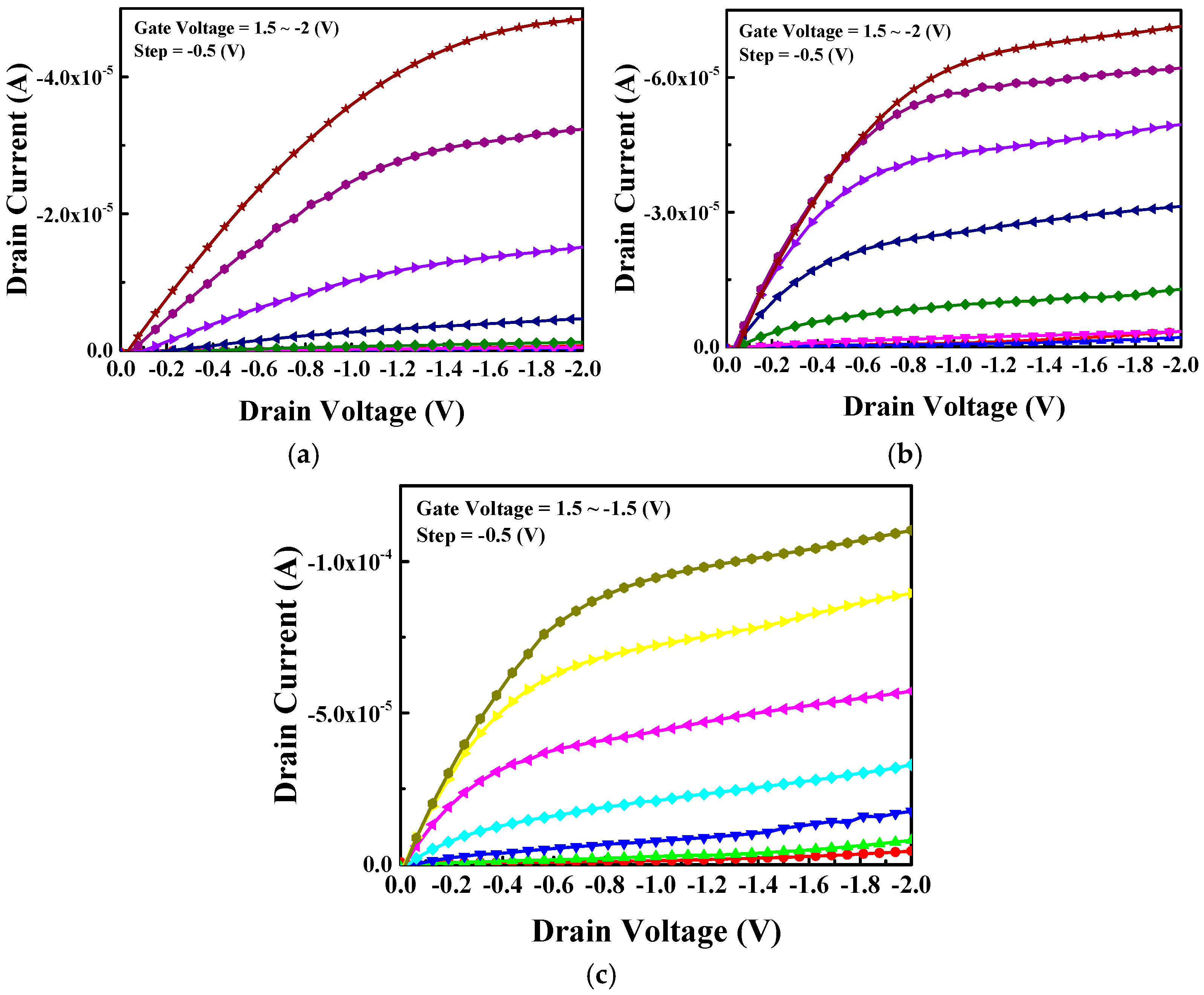
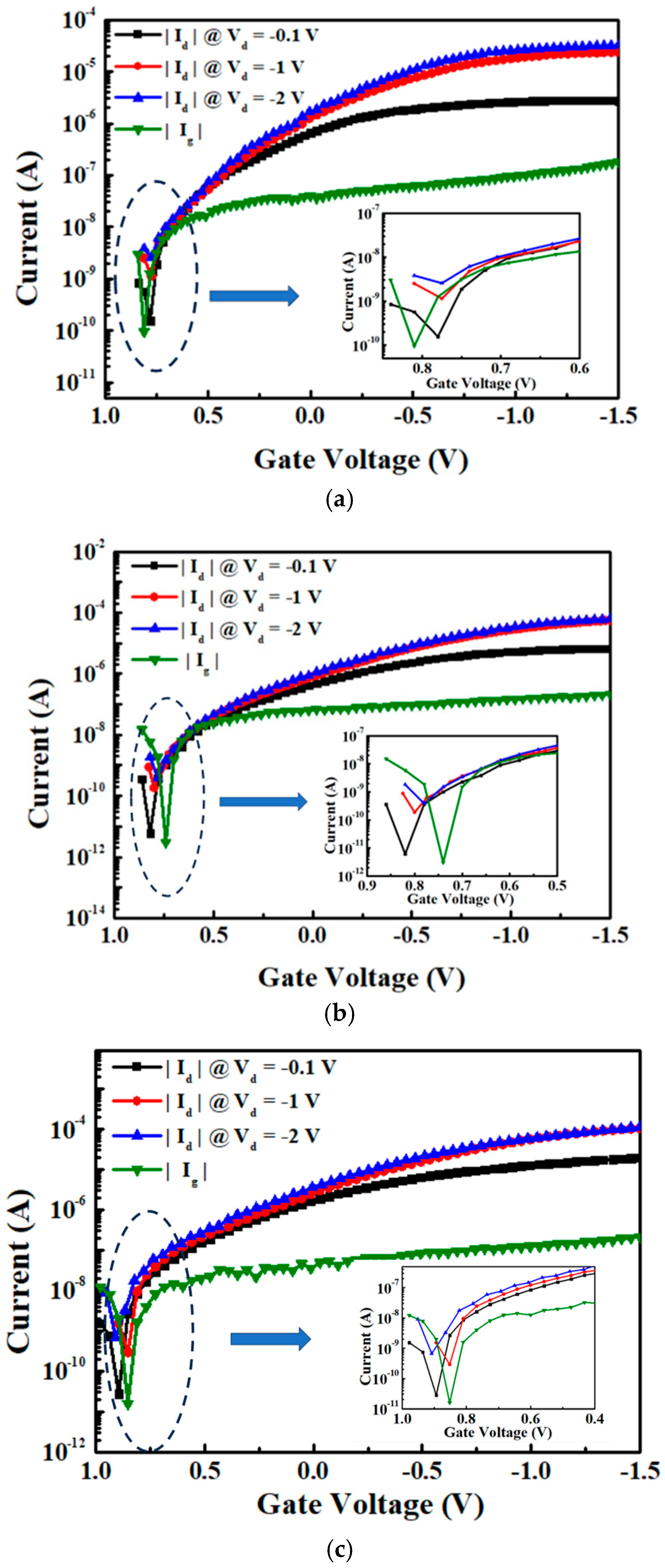
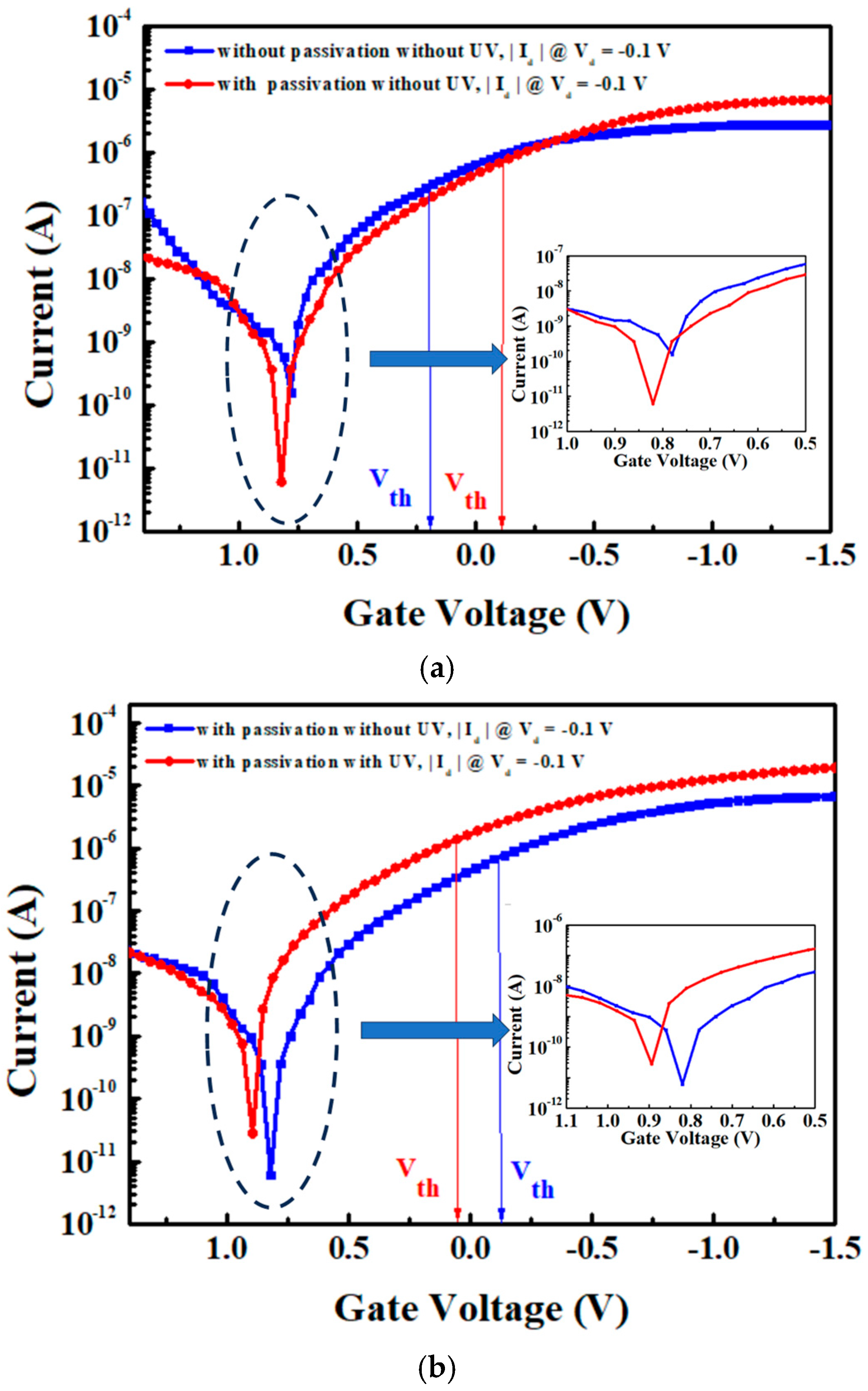
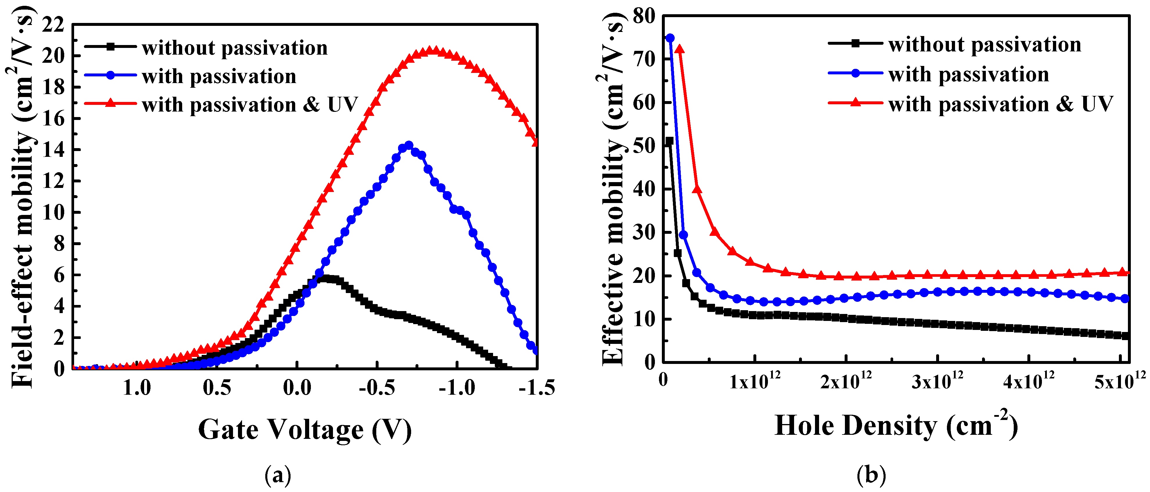
Four-inch p+ Si substrates were used. Then, 50 nm thick TiN was deposited and used as the gate electrode. The TiN was sputtered using a DC plasma source of 800 W, with an Ar flow rate of 100 sccm and a N2 flow rate of 5 sccm. Electron beam evaporation was employed to deposit a 45 nm thick HfO2 film and 6 nm thick SiO2 as the gate dielectric, with the deposition rate controlled at 0.2 Å/s. After deposition, the device underwent thermal anneal in a N2 environment at 400 °C for 1 h. After anneal, 7 nm thick SnO was sputtered using a DC plasma source at 25 W, with an Ar flow rate of 24 sccm, an O2 flow rate of 8 sccm, a chamber pressure of 7.6 mTorr, and a deposition rate of 0.1 Å/s. The device was annealed using rapid thermal anneal (RTA) at 200 °C in a N2 environment for 30 s. Next, 30 nm thick Ni was deposited on the SnO and served as the source and drain electrodes. Additionally, passivation layers consisting of a 5 nm thick SiO2 film, a 10 nm thick HfO2 film, and a 3 nm thick SiO2 film were deposited. The device had a channel length of 50 μm and a channel width of 500 μm. Finally, UV anneal was performed with 254 nm at a 79 mW/cm2 power and 185 nm at an 11 mW/cm2 power for 10 min. First-principles quantum mechanical calculations were conducted to study the electronic properties of SnO using Quantum-espresso, with both the generalized gradient approximation (GGA) and local-density approximations plus the Hubbard potential U (LDA + U) method.

3. Results

SnO has a lead oxide structure and crystallizes in the tetragonal P4/nmm space group. The structure is 2D and consists of one SnO sheet oriented in the (0, 0, 1) direction. In the SnO unit cell, each Sn2+ is bonded in a four-coordinate geometry to four equivalent O2− atoms. Each O2− is bonded to four equivalent Sn2+ atoms to form a mixture of corner- and edge-sharing OSn4 tetrahedra. First-principles quantum mechanical calculations using Quantum-espresso are used to study the band structure of SnO (Figure 1) and calculate the effective mass of the hole (mh*). SnO bandgaps of 0.62 eV and 0.18 m0 and an effective mass of the hole (mh*) at Γ points are obtained, as shown in Table 1.
Figure 2a represents oxygen vacancy formation or the dangling bonds in the SnO structure during film processing caused by a low oxygen partial pressure while using a metallic Sn target. Moreover, insufficient oxygen during deposition or anneal can prevent the complete oxidation of Sn, leaving excess Sn atoms that may occupy interstitial sites, as shown in Figure 2b. Figure 2c,d show that with SiO2 passivation, the oxygen dangling bonds of SiO2 at the SnO/SiO2 interface could potentially interact with oxygen-deficient sites in SnO. In Figure 2d, a SiOx transition layer forms at the interface between SiO2 and SnO. This SiOx originates from the low-temperature-deposited SiO2 side, either due to oxygen diffusion or the partial reduction of SiO2 during processing. The interface contains various charges, as follows: oxide-trapped charges deep in SiO2, fixed-oxide charges near the interface, and interface-trapped charges at the SiOx/SnO boundary. These charges can affect device behavior by shifting the threshold voltage and degrading carrier mobility. Such dielectric and interface charges have been well studied in metal/SiO2/Si MOS capacitors, which cause Coulomb scattering and FET mobility degradation in 2D material FETs.
Figure 3a,b show a schematic structural diagram and a transmission electron microscope (TEM) cross-sectional image of the passivated SnO device, respectively. From the TEM, the thickness of SnO is 7 nm, the bottom interfacial SiO2 is 6 nm, and the top passivated SiO2/HfO2/SiO2 layers are 5, 10, and 3 nm, respectively. The TEM image in Figure 3b was taken after anneal. Interface roughness can increase hole scattering, especially at a high charge density or effective field [19]. Interface charges at both the top and bottom SnO interfaces result in mobility degradation and a poor sub-threshold performance. To lower interface charge scattering, a 6 nm thick SiO2 layer is deposited in between the channel SnO and the gate dielectric HfO2 to reduce remote phonon scattering from the high-κ gate dielectric. After the deposition of HfO2 and SiO2, the device undergoes thermal anneal in a N2 environment at 400 °C for 1 h before SnO channel deposition. Thermal anneal at 400 °C in N2 improves the electrical quality of the HfO2 and SiO2 dielectrics, reduces interface trap states, and enhances mobility. To further lower top interface charge scattering, SiO2 passivation is also applied.
Figure 4 shows the capacitance density versus voltage (C-V) and current density versus voltage (J-V) characteristics of the Ni/6 nm SiO2/45 nm HfO2/TaN metal–insulator–metal (MIM) structure, which was made using the same mask as the SnO pFET. The capacitance density reaches 260 nF/cm2, which gives an overall high dielectric constant (high-κ) value of 15.0. The gate leakage current is only 4 × 10⁻⁶ A/cm2, attributed to the high-κ gate dielectric. The gate leakage current of metal-gate/high-κ/SnO is significantly higher than that in standard metal-gate/high-κ/single-crystal Si Complementary Metal–Oxide–Semiconductor (CMOS) FETs [20]. This is because the former is made at a limited temperature of 400 °C for backend-of-line (BEOL) processes while the latter is fabricated at 1000 °C. The limited thermal budget causes defects and trap-assisted leakage in the high-κ gate dielectric. To further decrease gate leakage current under low-temperature processing conditions, atomic layer deposition (ALD) can be employed; however, this involves a relatively long process time.
The FET’s µFE and µeff are obtained under a small drain voltage (Vd) [21], as follows:
μ F E = L W 1 C O X V d d I d d V g s m a l l   V d = L W 1 C O X V d g m s m a l l   V d   ,
μ e f f = L W g d q N i n v s m a l l   V d = L W g d C O X ( V g s V t h ) ,
where L and W are the channel length and width, Cox is the gate capacitance per unit area, gm is the transconductance, qNinv is the total induced Qh in the channel, and gd is the drain conductance, respectively. Here, µeff is essential for transistor modeling and crucial for IC design.
Figure 5a,b present the drain current versus Vd (|Id| − Vd) characteristics of nanosheet FETs, with 10 and 12 nm thick SnO channels, respectively. Both transistors show an increase in |Id| with an increasingly negative gate voltage (Vg), which indicates the pFET’s behavior. A good transistor pinch off is observed at a positive Vg. Additionally, the output |Id| is higher for the thicker SnO channel, suggesting enhanced hole conduction in the thicker SnO pFET. In Figure 5, the drain current continues to increase in the saturation regime. This increasing trend is not due to the gate leakage current, which is significantly lower than the drain current. Instead, it is attributed to the thicker SnO channel, which cannot be fully depleted by the gate electric field. To further reduce the gate leakage current under low-temperature processing conditions, ALD is a useful technique, although it involves a relatively long processing time.
Figure 6a–c show the |Id| − Vg, µFE − Vg, and µeff − Qh characteristics for 10 and 12 nm thick SnO pFETs. The 12 nm thick SnO pFET shows a superb transistor hole µeff of more than 100 cm2/V·s and 31.1 cm2/V·s at a Qh of 1 × 10¹¹ and 5 × 1012 cm−2, respectively. At a high 5 × 1012 cm−2 Qh, it is crucial to notice that the hole µeff increases from 27.3 cm2/V·s for the 10 nm thick SnO to 31.1 cm2/V·s for the 12 nm channel thickness. Although a higher µeff and output |Id| are obtained with the thicker SnO pFETs, there is a significant degradation in the IOFF. The large IOFF causes too high off-state leakage current and DC power consumption, which is intolerant for modern ICs with multi-billions of FETs. The high IOFF is attributed to the inability of the gate and surface potentials to fully deplete the thicker SnO channel. It is also noted that UV anneal does not alter the SnO film thickness, as confirmed by similar experiments performed on both SnO2 nFETs [16] and SnO pFETs [17].
Figure 7a–c show the |Id| − Vd characteristics for thinner 7 nm thick SnO pFETs under different device conditions, with and without passivation and with and without UV anneal. The increase in Id| with more −Vg confirms the p-type behavior of the FETs. At a Vg of −2 V, the output |Id| increases from the control device to the device with surface passivation and the pFET with both passivation and UV anneal. The |Id| curves do not increase monotonically with VG, which is due to the roll off of µeff with an increasing Qh [19].
Figure 8a–c present the |Id| − Vg characteristics of the 7 nm thick SnO device with and without passivation and with and without UV anneal. At Vd = −0.1 V, the SnO pFET with a passivation layer and UV anneal shows the highest |Id|. Such a higher |Id| is important for a higher-speed IC device.
Figure 9a shows the comparison of the |Id| − Vg characteristics for 7 nm thick SnO pFETs without UV anneal. The non-passivated control device exhibits an ION/IOFF of 1.8 × 10⁴, whereas the passivated device achieves a large 1.1 × 10⁶. The threshold voltages (Vth) extracted from the extrapolation of the Id linear region [22] are −0.1 and 0.2 V for the FETs without and with passivation, respectively. The two-orders-of-magnitude ION/IOFF improvement suggests that the passivation effectively isolates the channel surface from reacting with moisture. The SnO surface reaction with moisture further forms charged defects, which change the Vth and decrease the ION. Figure 9b shows the comparison of the |Id| − Vg characteristics between the control FET and the best-performing FET with passivation and UV anneal. The UV anneal further increases the ION/IOFF from 1.1 × 10⁶ to 6.9 × 10⁶. Such an improvement is attributed to the UV anneal effectively enhancing channel quality, thereby resulting in a superior electrical performance [17].
Figure 10a,b illustrate the µFE − Vg and µeff − Qh characteristics for 7 nm thick SnO pFETs, respectively. The peak µFE values increase from 5.8 and 14.3 to 20.3 cm2/V·s. The µeff values decrease from ~70 m2/V·s with an increasing Qh. At a Qh of 5 × 1012 cm−2, µeff increases from 6.1 and 14.7 to 20.7 cm2/V·s. This is the first time that the hole µeff of an oxide semiconductor has reached 20% of that of a single-crystal Si pFET at a 7 nm ultra-thin body thickness [23]. This improved pFET performance is due to both passivation and UV anneal, resulting in reduced defects and an improved quality of the SnO channel. Moreover, the interfacial charge trap density (Dit) [24] is calculated, and we find that passivated SnO with UV anneal has a Dit of 4.6 × 1012 cm−2 eV−1, close to that of passivated SnO (4.7 × 1012 cm−2 eV−1) and better than the SnO (8.2 × 1012 cm−2 eV−1). As shown in Figure 10a, the shoulder-like non-smooth µFE feature in the 7 nm thick SnO channel is attributed to extra scattering from defects, which can be improved by passivation and UV anneal. The shoulder-like non-smooth µFE feature in Figure 6a,b is due to a thicker SnO channel, where gate electric field cannot fully deplete the SnO channel and defects. This is confirmed by the higher ION/IOFF in thicker SnO channel pFETs.
Figure 11 presents the |Id| − Vg characteristics of 7 nm thick SnO pFETs as-fabricated and after two months of exposure to air. The control device shows significant deterioration after exposure to air, and the µFE decreases from 5.8 to 1.5 cm2/V·s after 2 months. In contrast, the device with passivation exhibits minimal changes in electrical performance as follows: the passivated and non-UV annealed device decreases from 14.3 to 12.3 cm2/V·s, and the passivated and UV-annealed device decreases slightly from 20.3 to 19.2 cm2/V·s. This comparison highlights the significant impact of passivation and channel material quality on device performance. The device shown in Figure 11a is not encapsulated to show the aging effect. The unpassivated control device exhibits significant degradation after two months of air exposure, with the μFE dropping from 5.8 to 1.5 cm2/V·s. In contrast, the passivated device only shows a minimal decline from 20.3 to 19.2 cm2/V·s, highlighting the strong protective role of a passivation approach. For future practical integration into ICs, external encapsulation using SiN will be applied to top Cu and low-κ interconnecting BEOL layers to improve long-term stability. However, SiO2 passivation directly on SnO pFETs must still be applied to prevent any moisture-related degradation during BEOL processes.
To further understand such an excellent performance, the SnO channels are characterized by X-ray photoelectron spectroscopy (XPS) [25,26]. The XPS results are calibrated using the C1s binding energy peak at 284.4 eV as a reference. Figure 12 shows the XPS Sn 3d5/2 peaks for SnO pFETs under different conditions. The Sn 3d5/2 peaks can be categorized into the following three types: Sn0 at 484.1 eV, Sn2+ at 486.3 eV, and Sn4+ at 486.9 eV [16,27]. Table 2 summarizes the deconvoluted Sn 3d5/2 XPS of Sn0, Sn2+, and Sn4+. Because the lattice energies of SnO2 (11,807 kJ mol−1) are much higher than those of SnO (3652 kJ mol−1), surface SnO can react with oxygen and moisture in air to form SnO1+x [28]. Consequently, when passivation and UV anneal are applied, the proportion of Sn2+ increases from 65.2% to 73.8% and Sn4+ decreases from 27.7% to 16.5%.
Table 3 summarizes the performance comparison between this study and other SnO pFET devices published in the literature. By applying passivation and UV anneal to SnO, the sub-threshold swing (SS) value is improved to 231 mV/dec compared with SnO (358 mV/dec) and passivated SnO (233 mV/dec). Our SnO pFETs provide the best ION/IOFF near seven orders of magnitude, one of the lowest IOFF, a small SS, and a remarkably high µeff for high-speed and for low-power applications. Device reproducibility has been demonstrated in our previous publications [13,17,29]. The μeff of 20.7 cm2/V·s is the highest value obtained for a SnO pFET with a typical standard deviation of 3.4 for 10 devices [13] and an ION/IOFF of 6.9 × 10⁶ with a standard deviation of 87. This level of device variability is comparable to that observed in our previously reported SnON nFETs [2].

4. Conclusions

In this study, we investigated the electrical performance and material properties of the following three types of devices: devices without a passivation layer and without UV anneal, devices with a passivation layer but without UV anneal, and devices with both a passivation layer and UV anneal. From XPS, the SnO with a passivation layer and UV anneal showed a reduced Sn4+ ratio and increased Sn2+, which resulted in an ION/IOFF as high as 6.94 × 10⁶ and an effective mobility of up to 20.7 cm2/V·s at a hole density (Qh) of 5 × 1012 cm−2 in the pFET. These results indicate that this nanosheet SnO FET meets the requirements of simple, low-cost, and low-temperature fabrication, and will be useful for future monolithic 3D CFET applications.

Author Contributions

Conceptualization, K.-C.C. and A.C.; methodology, K.-C.C. and J.W.; software, P.P.; validation, K.-C.C., J.W., P.P. and A.C.; formal analysis, K.-C.C., J.W. and P.P.; investigation, K.-C.C.; writing—original draft preparation, K.-C.C. and J.W.; writing—review and editing, P.P. and A.C.; supervision, A.C. All authors have read and agreed to the published version of the manuscript.

Funding

This work was supported by the National Science and Technology Council of Taiwan [Project no. 113-2221-E-A49-100 and 113-2811-E-A49-534] for the research.

Data Availability Statement

The data presented in this study are available on request from the corresponding author. The data are not publicly available due to privacy.

Acknowledgments

We would like to thank the National Yang Ming Chiao Tung University Nano Facility Center for providing the laboratory instruments.

Conflicts of Interest

The authors declare no conflicts of interest.

References

  1. Nomura, K.; Ohta, H.; Takagi, A.; Kamiya, T.; Hirano, M.; Hosono, H. Room-temperature fabrication of transparent flexible thin-film transistors using amorphous oxide semiconductors. Nature 2004, 432, 488–492. [Google Scholar] [CrossRef] [PubMed]
  2. Pooja, P.; Che, C.C.; Zeng, S.H.; Lee, Y.C.; Yen, T.J.; Chin, A. Outstanding high field-effect mobility of 299 cm2 V−1s−1 by nitrogen-doped SnO2 nanosheet thin-film transistor. Adv. Mater. Technol. 2023, 8, 2201521. [Google Scholar] [CrossRef]
  3. Li, S.L.; Wakabayashi, K.; Xu, Y.; Nakaharai, S.; Komatsu, K.; Li, W.W.; Lin, Y.F.; Aparecido-Ferreira, A.; Tsukagoshi, K. Thickness-dependent interfacial coulomb scattering in atomically thin field-effect transistors. Nano Lett. 2013, 13, 3546–3552. [Google Scholar] [CrossRef]
  4. Bai, Z.; He, D.; Fu, S.; Miao, Q.; Liu, S.; Huang, M.; Zhao, K.; Wang, Y.; Zhang, X. Recent progress in electron–phonon interaction of two-dimensional materials. Nano Select 2022, 3, 1112–1122. [Google Scholar] [CrossRef]
  5. Chang, H.; Huang, C.H.; Matsuzaki, K.; Nomura, K. Back-channel defect termination by sulfur for p-channel Cu2O thin-film transistors. ACS Appl. Mater. Interfaces 2020, 12, 51581–51588. [Google Scholar] [CrossRef]
  6. Hsu, S.M.; He, J.C.; Li, Y.S.; Su, D.Y.; Tsai, F.Y.; Cheng, I.C. Effect of mechanical strain on electrical performance of flexible P-type SnO thin-film transistors. IEEE Trans. Electron Devices 2019, 66, 5183–5186. [Google Scholar] [CrossRef]
  7. Chae, M.G.; Kim, J.; Jang, H.W.; Park, B.K.; Chung, T.M.; Kim, S.K.; Han, J.H. High field-effect mobility and on/off current ratio of p-type ALD SnO thin-film transistor. ACS Appl. Electron. Mater. 2023, 5, 1992–1999. [Google Scholar] [CrossRef]
  8. Ahmed, S.; Shahid, M.M.; Bakar, S.A.; Arshed, N.; Basirun, W.J.; Fouad, H. Fabrication and Characterization of SnO–Cu2O Mixed Metal Oxide Thin Films for Photoelectrochemical Applications. J. Nanosci. Nanotechnol. 2020, 20, 7705–7709. [Google Scholar] [CrossRef]
  9. Liu, A.; Liu, G.; Zhu, H.; Shin, B.; Fortunato, E.; Martins, R.; Shan, F. Hole mobility modulation of solution-processed nickel oxide thin-film transistor based on high-k dielectric. Appl. Phys. Lett. 2016, 108, 233506. [Google Scholar] [CrossRef]
  10. Caraveo-Frescas, J.A.; Nayak, P.K.; Al-Jawhari, H.A.; Granato, D.B.; Schwingenschlogl, U.; Alshareef, H.N. Record mobility in transparent p-type tin monoxide films and devices by phase engineering. ACS Nano 2013, 7, 5160–5167. [Google Scholar] [CrossRef]
  11. Caraveo-Frescas, J.A.; Alshareef, H.N. Transparent p-type SnO nanowires with unprecedented hole mobility among oxide semiconductors. Appl. Phys. Lett. 2013, 103, 222103. [Google Scholar] [CrossRef]
  12. Ogo, Y.; Hiramatsu, H.; Nomura, K.; Yanagi, H.; Kamiya, T.; Hirano, M.; Hosono, H. P-channel thin-film transistor using p-type oxide semiconductor, SnO. Appl. Phys. Lett. 2008, 93, 032113. [Google Scholar] [CrossRef]
  13. Shih, C.W.; Chin, A.; Lu, C.F.; Su, W.F. Remarkably high hole mobility metal-oxide thin-film transistors. Sci. Rep. 2018, 8, 889. [Google Scholar] [CrossRef]
  14. Hu, Y.; Schlom, D.; Datta, S.; Cho, K. Interlayer engineering of band gap and hole mobility in p-type oxide SnO. ACS Appl. Mater. Interfaces 2022, 14, 25670–25679. [Google Scholar] [CrossRef]
  15. Pan, X.; Fu, L. Oxidation and phase transitions of epitaxial tin oxide thin films on (1012) sapphire. J. Appl. Phys. 2001, 89, 6048–6055. [Google Scholar] [CrossRef]
  16. Shih, C.W.; Chin, A.; Lu, C.F.; Su, W.F. Low-temperature processed tin oxide transistor with ultraviolet irradiation. IEEE Electron Device Lett. 2019, 40, 909–912. [Google Scholar] [CrossRef]
  17. Zeng, S.H.; Pooja, P.; Wu, J.; Chin, A. Impact of UV annealing on the hole effective mobility in SnO pFET. Sci. Rep. 2024, 14, 26256. [Google Scholar] [CrossRef] [PubMed]
  18. Zhang, Y. Thermal oxidation fabrication of NiO film for optoelectronic devices. Appl. Surf. Sci. 2015, 344, 33–37. [Google Scholar] [CrossRef]
  19. Takagi, S.I.; Toriumi, A.; Iwase, M.; Tango, H. On the universality of inversion layer mobility in Si MOSFET’s: Part I-effects of substrate impurity concentration. IEEE Trans. Electron Devices 1994, 41, 2357–2362. [Google Scholar] [CrossRef]
  20. Huang, C.H.; Yu, D.S.; Chin, A.; Wu, C.H.; Chen, W.J.; Zhu, C.X.; Li, M.F.; Cho, B.J.; Kwong, D.L. Fully silicided NiSi and germanided NiGe dual gates on SiO2/Si and Al2O3/Ge-on-insulator MOSFETs. In Proceedings of the IEEE International Electron Devices Meeting 2003, Washington, DC, USA, 8–10 December 2003; pp. 319–322. [Google Scholar]
  21. Sun, S.; Plummer, J.D. Electron mobility in inversion and accumulation layers on thermally oxidized silicon surfaces. IEEE Trans. Electron Devices 1980, 27, 1497–1508. [Google Scholar] [CrossRef]
  22. Schroder, D.K. Semiconductor Material and Device Characterization; John Wiley & Sons: Hoboken, NJ, USA, 2015. [Google Scholar]
  23. Kobayashi, S.; Saitoh, M.; Uchida, K. More-than-universal mobility in double-gate SOI p-FETs with sub-10-nm body thickness -role of light-hole band and compatibility with uniaxial stress engineering. In Proceedings of the 2007 IEEE International Electron Devices Meeting, Washington, DC, USA, 10–12 December 2007; pp. 707–710. [Google Scholar]
  24. Cai, W.; Park, S.; Zhang, J.; Wilson, J.; Li, Y.; Xin, Q.; Majewski, L.; Song, A. One-volt IGZO thin-film transistors with ultra-thin, solution-processed AlxOy gate dielectric. IEEE Electron Device Lett. 2018, 39, 375–378. [Google Scholar] [CrossRef]
  25. Yakuphanoglu, F. Electrical conductivity, seebeck coefficient and optical properties of SnO2 film deposited on ITO by dip coating. J. Alloys Compd. 2009, 470, 55–59. [Google Scholar] [CrossRef]
  26. Jia, J.; Sugane, T.; Nakamura, S.I.; Shigesato, Y. P-type conduction mechanism in continuously varied non-stoichiometric SnOx thin films deposited by reactive sputtering with the impedance control. J. Appl. Phys. 2020, 127, 185703. [Google Scholar] [CrossRef]
  27. Kim, J.H.; Jeon, K.M.; Park, J.S.; Kang, Y.C. Excellent Li-ion storage performances of hierarchical SnO-SnO2 composite powders and SnO nanoplates prepared by one-pot spray pyrolysis. J. Power Sources 2017, 359, 363–370. [Google Scholar] [CrossRef]
  28. Tyckoson, D. CRC Handbook of Chemistry and Physics, 95th ed.; Chicago Booklist Publications: Boca Raton, FL, USA, 1998; p. 689. [Google Scholar]
  29. Yen, T.J.; Chin, A.; Gritsenko, V. Exceedingly high performance top-gate p-type SnO thin film transistor with a nanometer scale channel layer. Nanomaterials 2021, 11, 92. [Google Scholar] [CrossRef]
  30. Kim, H.M.; Choi, S.H.; Jeong, H.J.; Lee, J.H.; Kim, J.; Park, J.S. Highly dense and stable p-type thin-film transistor based on atomic layer deposition SnO fabricated by two-step crystallization. ACS Appl. Mater. Interfaces 2021, 13, 30818–33082. [Google Scholar] [CrossRef]
  31. Kim, H.M.; Choi, S.H.; Lee, H.U.; Cho, S.B.; Park, J.S. The significance of an in situ ALD Al2O3 stacked structure for p-type SnO TFT performance and monolithic all-ALD-channel CMOS inverter applications. Adv. Electron. Mater. 2023, 9, 2201202. [Google Scholar] [CrossRef]
  32. Lu, J.; Shen, M.; Feng, X.; Tan, T.; Guo, H.; Lin, L.; Zhou, F.; Li, Y. P-type oxide thin-film transistor with unprecedented hole field-effect mobility for an all-oxide CMOS CFET-like inverter suitable for monolithic 3D integration. Nano Lett. 2024, 24, 15260–15267. [Google Scholar] [CrossRef]
  33. Lee, J.H.; Kim, J.; Jin, M.; Na, H.J.; Lee, H.; Im, C.; Kim, Y.S. Cu2O p-type thin-film transistors with enhanced switching characteristics for CMOS logic circuit by controlling deposition condition and annealing in the N2 atmosphere. ACS Appl. Electron. Mater. 2023, 5, 1123–1130. [Google Scholar] [CrossRef]
  34. Lin, C.W.; Chung, W.C.; Zhang, Z.D.; Hsu, M.C. P-channel transparent thin-film transistor using physical-vapor-deposited NiO layer. Jpn. J. Appl. Phys. 2017, 57 (Suppl. S1), 01AE01. [Google Scholar] [CrossRef]
  35. Mashooq, K.; Jo, J.; Peterson, R.L. Effect of metal capping layer in achieving record high p-type SnO thin film transistor mobility. IEEE Trans. Electron Devices 2023, 71, 574–580. [Google Scholar] [CrossRef]
  36. Chen, Y.; Sun, Y.; Dai, X.; Zhang, B.; Ye, Z.; Wang, M.; Wu, H. Tunable electrical properties of NiO thin films and p-type thin-film transistors. Thin Solid Films 2015, 592, 195–199. [Google Scholar] [CrossRef]
  37. Shan, F.; Liu, A.; Zhu, H.; Kong, W.; Liu, J.; Shin, B.; Fortunato, E.; Martins, R.; Liu, G. High-mobility p-type NiOx thin-film transistors processed at low temperatures with Al2O3 high-k dielectric. J. Mater. Chem. C 2016, 4, 9438–9444. [Google Scholar] [CrossRef]
  38. Han, S.; Niang, K.M.; Rughoobur, G.; Flewitt, A.J. Effects of post-deposition vacuum annealing on film characteristics of p-type Cu2O and its impact on thin film transistor characteristics. Appl. Phys. Lett. 2016, 109, 173502. [Google Scholar] [CrossRef]
  39. Singh, V.; Sinha, J.; Avasthi, S. Two-step process using MOCVD and thermal oxidation to obtain pure-phase Cu2O thin films transistors. ACS Appl. Electron. Mater. 2021, 4, 367–374. [Google Scholar] [CrossRef]
  40. Kim, S.Y.; Ahn, C.H.; Lee, J.H.; Kwon, Y.H.; Hwang, S.; Lee, J.Y.; Cho, H.K. P-channel oxide thin film transistors using solution-processed copper oxide. ACS Appl. Mater. Interfaces 2013, 5, 2417–2421. [Google Scholar] [CrossRef]
  41. Bae, J.H.; Lee, J.H.; Park, S.P.; Jung, T.S.; Kim, H.J.; Kim, D.; Lee, S.W.; Park, K.S.; Yoon, S.; Kang, I.; et al. Gallium doping effects for improving switching performance of p-type copper (I) oxide thin-film transistors. ACS Appl. Mater. Interfaces 2020, 12, 38350–38356. [Google Scholar] [CrossRef]
Figure 1. Energy band structure of SnO. CBM and VBM represent conduction band minimum and valence band maximum, respectively.
Nanomaterials 15 00640 g001
Figure 2. SnO structure with (a) oxygen vacancies (dangling bonds), (b) Sn interstitial, (c) SiO2 passivation, and (d) interface charges.
Nanomaterials 15 00640 g002
Figure 3. (a) Schematic diagram and (b) TEM cross-sectional image of the SnO transistor structure with a passivation layer.
Nanomaterials 15 00640 g003
Figure 4. C-V at 1 kHz and J-V characteristics of the Ni/6 nm SiO2/45 nm HfO2/TaN capacitor.
Nanomaterials 15 00640 g004
Figure 5. |Id| − Vd characteristics of passivated and UV-annealed SnO nanosheet pFETs with (a) 10 nm and (b) 12 nm thick SnO channel.
Nanomaterials 15 00640 g005
Figure 6. (a) |Id| − Vg and µFE − Vg characteristics of (a) 10 nm and (b) 12 nm thick SnO channel FETs. (c) µeff − Qh characteristics of passivated and UV-annealed pFETs with 10 and 12 nm SnO thicknesses.
Nanomaterials 15 00640 g006
Figure 7. |Id| − Vd characteristics for 7 nm thick SnO pFETs (a) without passivation and UV anneal, (b) with passivation but without UV anneal, and (c) with passivation and UV anneal.
Nanomaterials 15 00640 g007
Figure 8. |Id| − Vg characteristics for 7 nm thick SnO pFETs in linear and saturation region of (a) control device without passivation or UV anneal, (b) with passivation but without UV anneal, and (c) with passivation and UV anneal (inset shows magnified |Id| and |Ig| near IOFF).
Nanomaterials 15 00640 g008
Figure 9. Comparison of |Id| − Vg characteristics for 7 nm thick SnO pFETs (a) without (control) and with passivated pFETs, and (b) control and the best device with passivation and UV anneal (inset shows magnified |Id| near IOFF).
Nanomaterials 15 00640 g009
Figure 10. (a) µFE − Vg and (b) µeff − Qh characteristics for 7 nm thick SnO pFETs.
Nanomaterials 15 00640 g010
Figure 11. |Id| − Vg characteristics for 7-nm thick SnO pFETs (a) control device without passivation or UV anneal, (b) with passivation but without UV anneal, and (c) with passivation and with UV anneal. The devices were measured as-fabricated and after exposure to air for two months.
Nanomaterials 15 00640 g011
Figure 12. XPS Sn 3d5/2 peaks of SnO pFET (a) w/o passivation w/o UV, (b) w/o passivation w/o UV, (c) w/i passivation w/o UV, and (d) w/i passivation w/i UV.
Nanomaterials 15 00640 g012
Table 1. Comparison table of p-type metal–oxide–semiconductors.
P-TypeEgHole Effective Mass (mh*)
SnO 0.62 eV (Indirect)0.18 m0
Cu2O [13]2.1 eV (Direct)0.65 m0
NiO [18]3.6 eV (Indirect)0.45 m0
Table 2. Summary of Sn3d5/2 proportions.
SampleSn0Sn2+Sn4+
SnO7.1%65.2%27.7%
SnO_UV6.3%62.4%31.3%
Passivated SnO9.3%68.9%21.8%
Passivated SnO_UV9.7%73.8%16.5%
Table 3. Comparison of SnO pFET performance.
Refs.ChannelIOFF
(A/μm)
ION/IOFFSS (mV/dec)µFE
(cm2/V·s)
µeff
(cm2/V·s)
Tech. and Anneal
This workSnO5.6 × 10−146.9 × 10623120.320.7200 °C RTA
SiO2 passivation
UV anneal
[12]SnO-~102-1.3-200 °C RTA
[10]SnO~10−126 × 10376306.75-180 °C 30 min
[11]SnO~4 × 10⁻¹⁰>10376010.83-160 °C
[30]SnO-2.7 × 10246006-300 °C 1 h
[31]SnO-6.54 × 1051501.14-300 °C 1 h
[32]SnO-2.5 × 103240.938.7-175 °C 2 h
[17]SnO~2.5 × 10−131.05 × 10527413.3313.38200 °C RTA
UV anneal
[33]Cu2O-4.68 × 10439101.11-Thermal anneal 800 °C 1 h
[5]Cu2O-4.1 × 10623501.38-100 °C 1 h
[34]NiO2.75 × 10−73.61 × 10⁴-1.09-200 °C 30 min
[9]NiO-1052504.4-250 °C
[35]SnO-4.2 × 103610017.219.1300 °C 1 h
[36]NiO-10326001.07--
[37]NiOx-10570025-UV treatment, 40 min and anneal 350 °C 1 h
[38]Cu2O-3.4 × 10226,0000.9-700 °C
[39]Cu2O---4.3 × 10⁻²-650 °C oxidation
[40]Cu2O-102-0.16-400 °C 30 min
[41]Ga-doped Cu2O-1.22 × 10477200.74-800 °C
Disclaimer/Publisher’s Note: The statements, opinions and data contained in all publications are solely those of the individual author(s) and contributor(s) and not of MDPI and/or the editor(s). MDPI and/or the editor(s) disclaim responsibility for any injury to people or property resulting from any ideas, methods, instructions or products referred to in the content.

