Environmental Effects on the Electrical Characteristics of Back-Gated WSe2 Field-Effect Transistors

 ,
,  ,
, 
Abstract
:1. Introduction
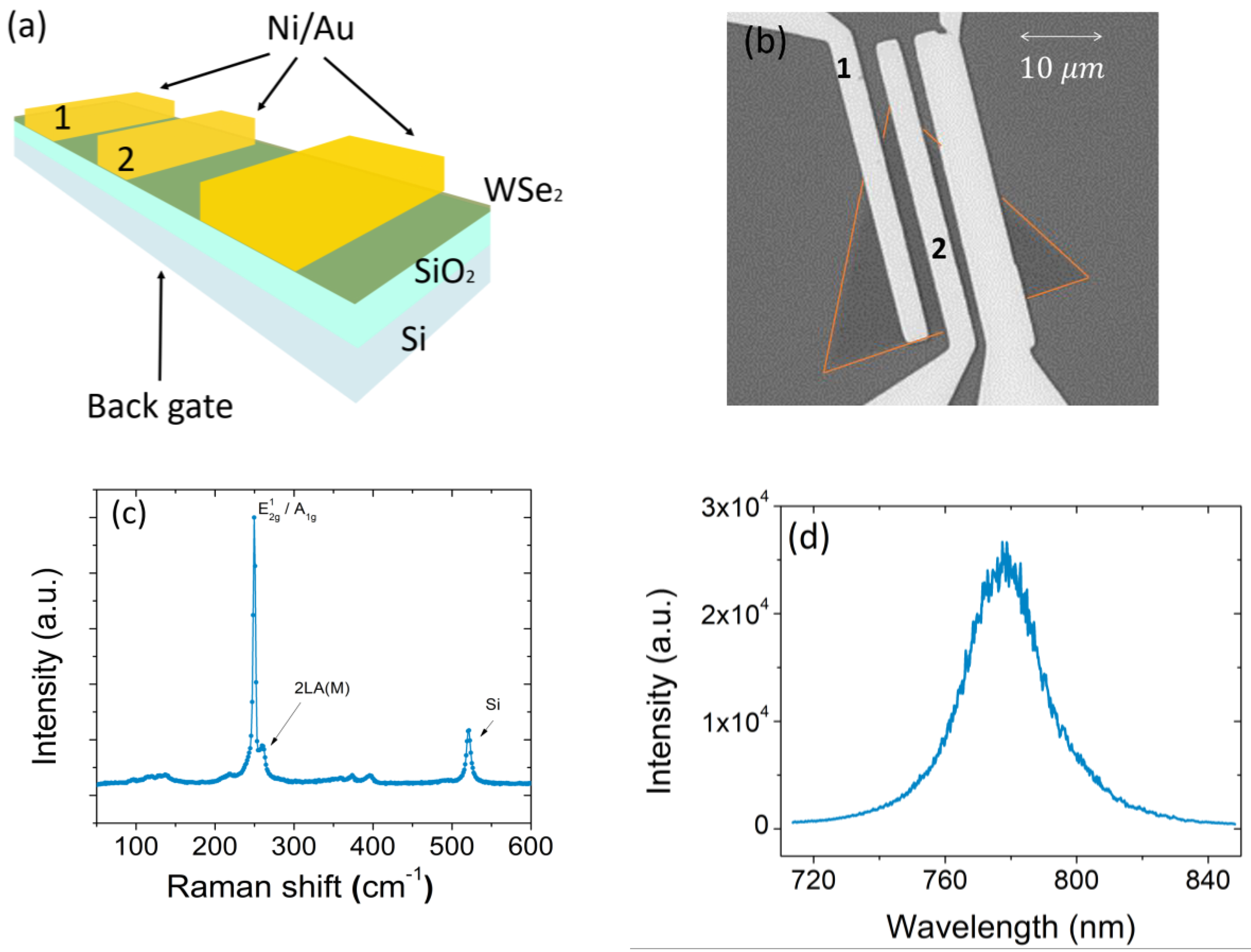
2. Experimental
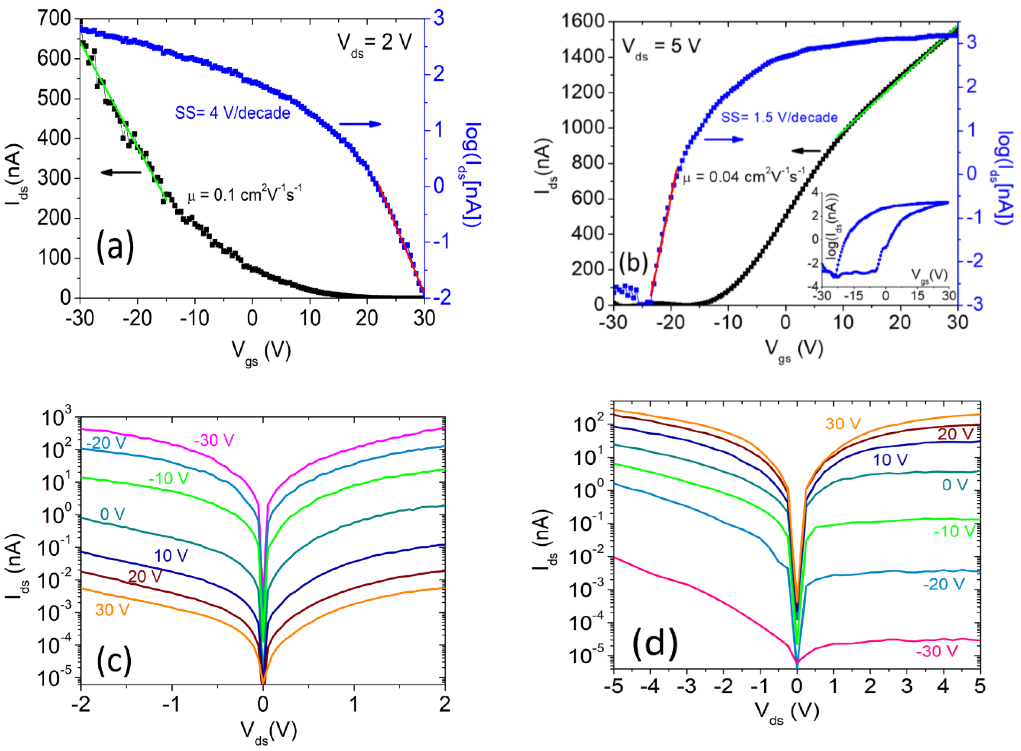
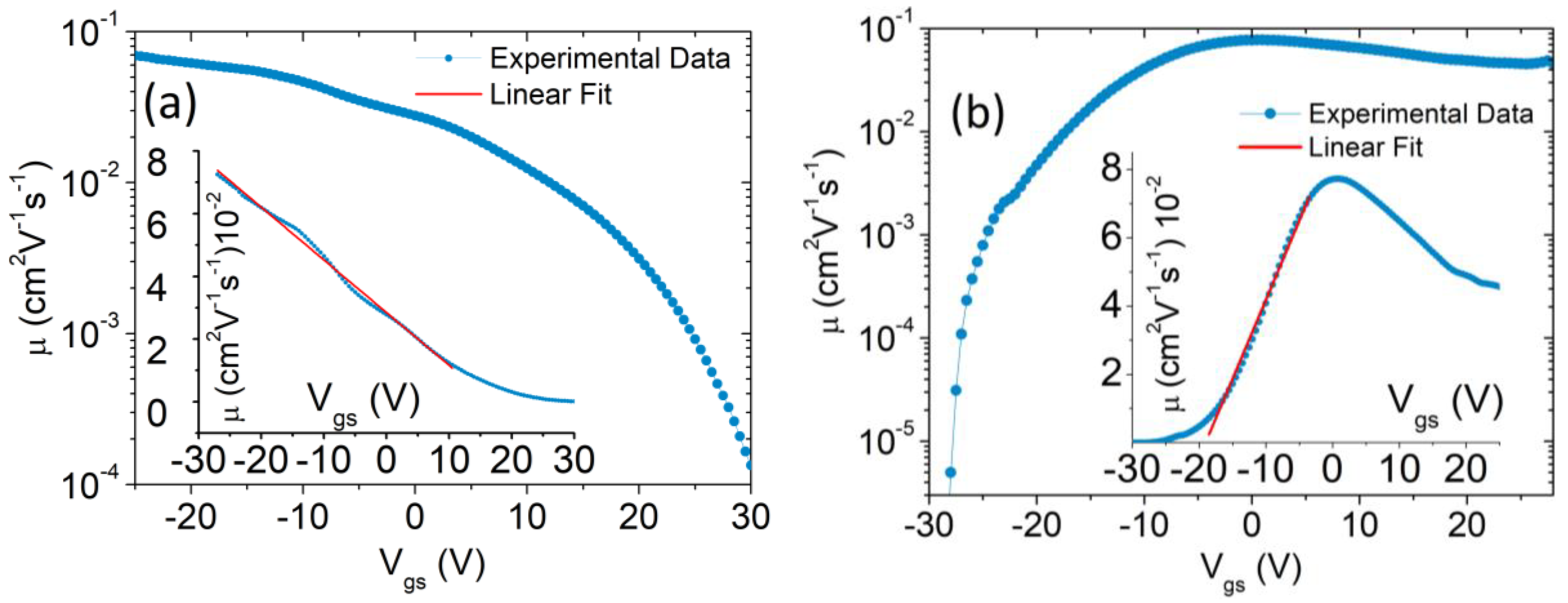
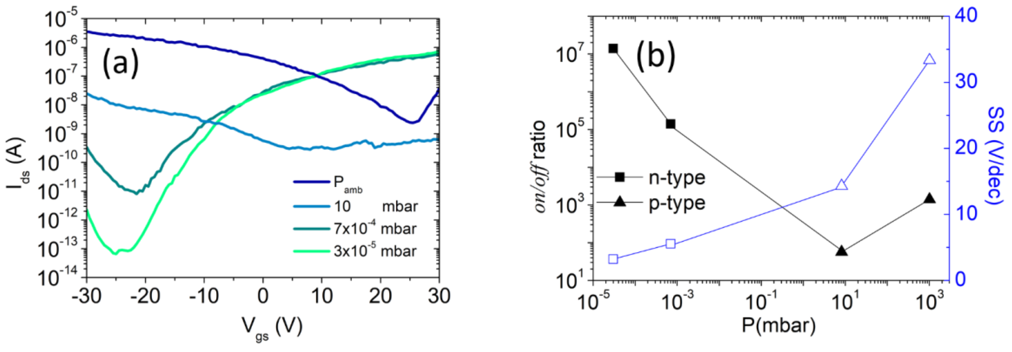
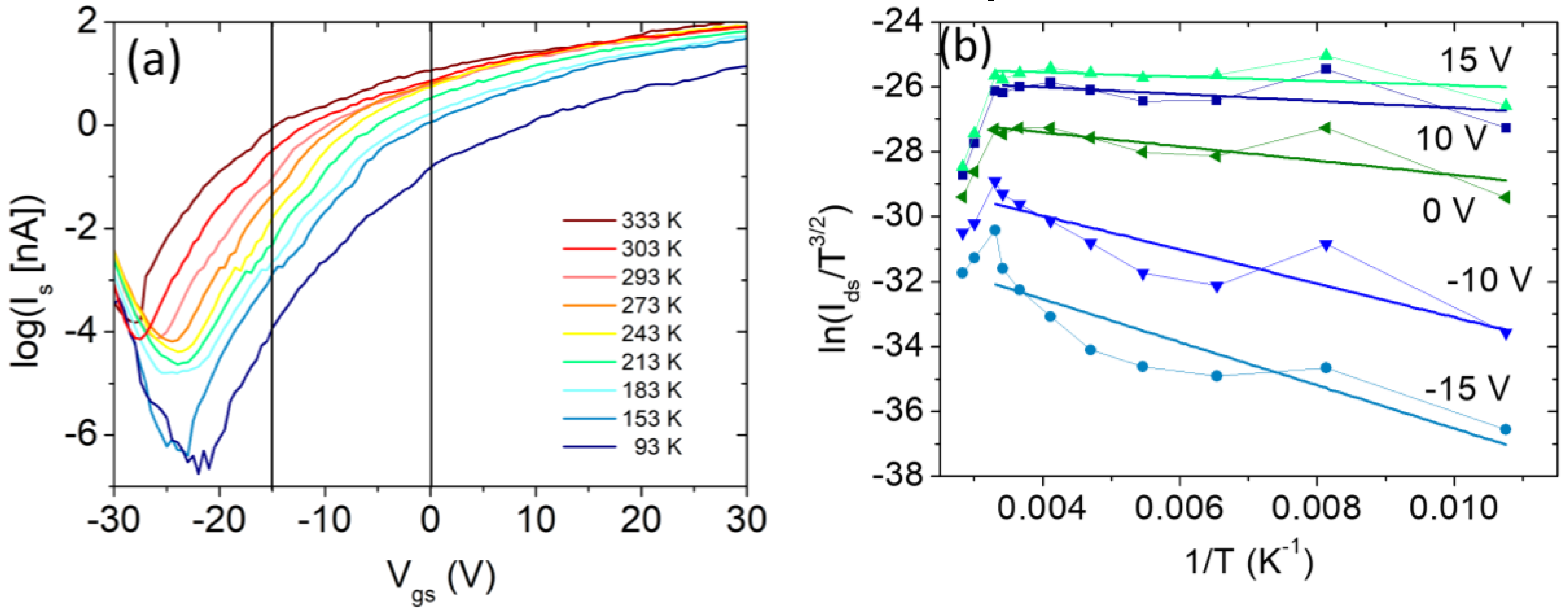
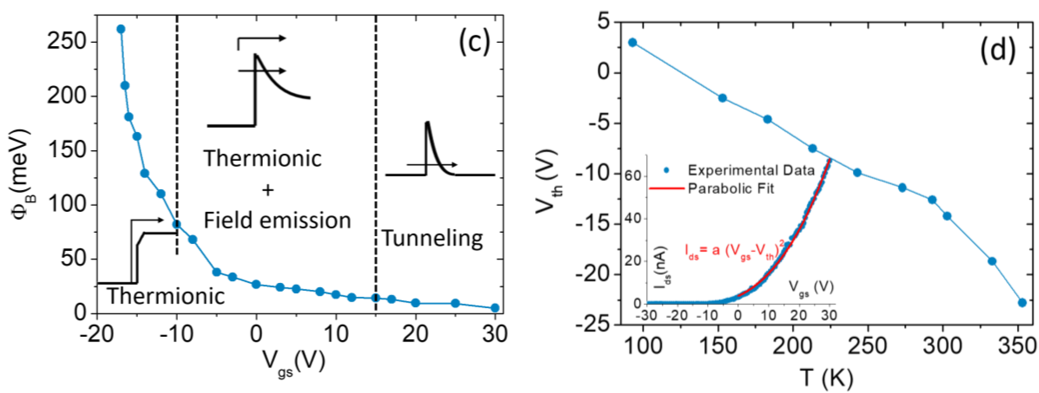
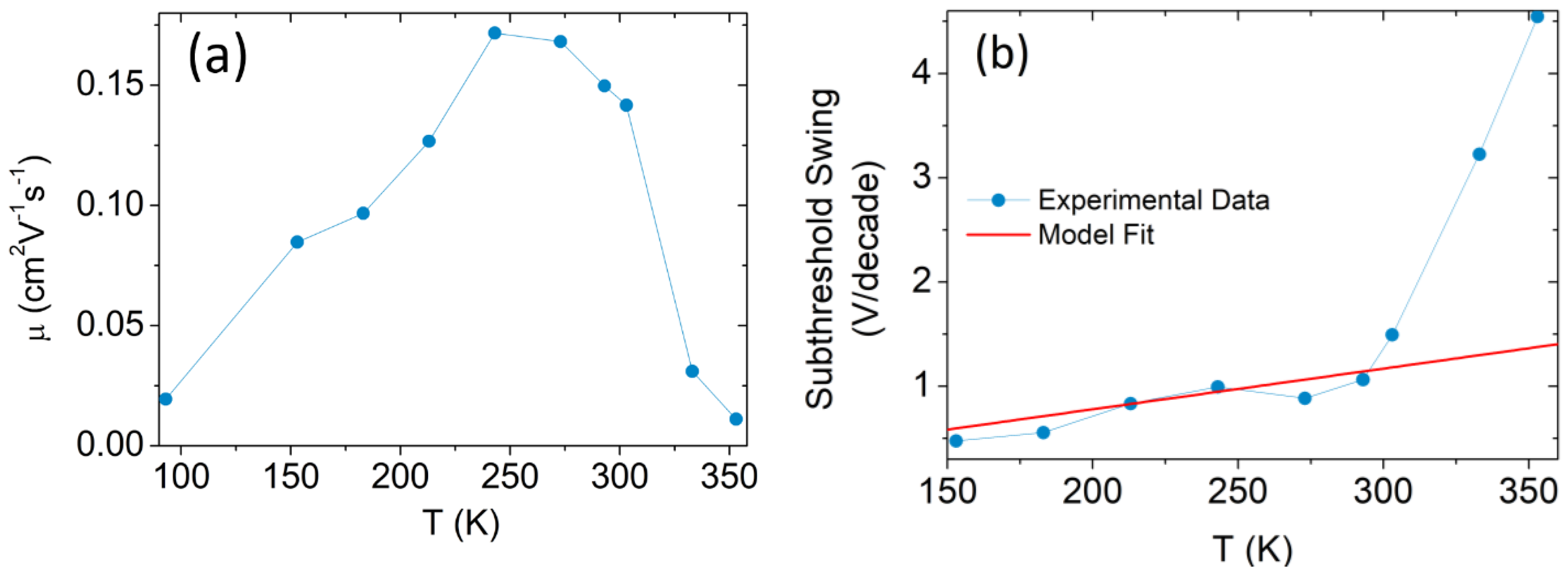
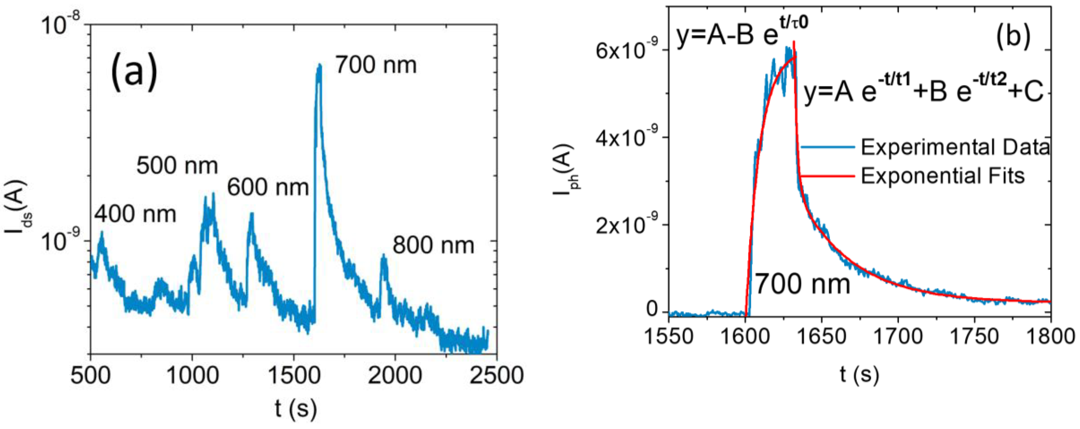
3. Results and Discussion
4. Conclusions
Author Contributions
Funding
Conflicts of Interest
References
- Georgiou, T.; Jalil, R.; Belle, B.D.; Britnell, L.; Gorbachev, R.V.; Morozov, S.V.; Kim, Y.-J.; Gholinia, A.; Haigh, S.J.; Makarovsky, O.; et al. Vertical field-effect transistor based on graphene–WS2 heterostructures for flexible and transparent electronics. Nat. Nanotechnol. 2012, 8, 100–103. [Google Scholar] [CrossRef] [PubMed]
- Liu, H.; Neal, A.T.; Ye, P.D. Channel length scaling of MoS2 MOSFETs. ACS Nano 2012, 6, 8563–8569. [Google Scholar] [CrossRef] [PubMed]
- Lopez-Sanchez, O.; Lembke, D.; Kayci, M.; Radenovic, A.; Kis, A. Ultrasensitive photodetectors based on monolayer MoS2. Nat. Nanotechnol. 2013, 8, 497. [Google Scholar] [CrossRef] [PubMed]
- Pospischil, A.; Furchi, M.M.; Mueller, T. Solar-energy conversion and light emission in an atomic monolayer p–n diode. Nat. Nanotechnol. 2014, 9, 257. [Google Scholar] [CrossRef] [PubMed]
- Radisavljevic, B.; Radenovic, A.; Brivio, J.; Giacometti, V.; Kis, A. Single-layer MoS2 transistors. Nat. Nanotechnol. 2011, 6, 147. [Google Scholar] [CrossRef] [PubMed]
- Baugher, B.W.H.; Churchill, H.O.H.; Yang, Y.; Jarillo-Herrero, P. Optoelectronic devices based on electrically tunable p–n diodes in a monolayer dichalcogenide. Nat. Nanotechnol. 2014, 9, 262. [Google Scholar] [CrossRef] [PubMed]
- Ross, J.S.; Klement, P.; Jones, A.M.; Ghimire, N.J.; Yan, J.; Mandrus, D.G.; Taniguchi, T.; Watanabe, K.; Kitamura, K.; Yao, W.; et al. Electrically tunable excitonic light-emitting diodes based on monolayer WSe2 p–n junctions. Nat. Nanotechnol. 2014, 9, 268. [Google Scholar] [CrossRef] [PubMed]
- Liu, W.; Kang, J.; Sarkar, D.; Khatami, Y.; Jena, D.; Banerjee, K. Role of metal contacts in designing high-performance monolayer n-type WSe2 field effect transistors. Nano Lett. 2013, 13, 1983–1990. [Google Scholar] [CrossRef] [PubMed]
- Guo, Y.; Han, Y.; Li, J.; Xiang, A.; Wei, X.; Gao, S.; Chen, Q. Study on the resistance distribution at the contact between molybdenum disulfide and metals. ACS Nano 2014, 8, 7771–7779. [Google Scholar] [CrossRef] [PubMed]
- Rai, A.; Movva, C.H.; Roy, A.; Taneja, D.; Chowdhury, S.; Banerjee, K.S. Progress in contact, doping and mobility engineering of MoS2: An atomically thin 2D semiconductor. Crystals 2018, 8, 316. [Google Scholar] [CrossRef]
- Dean, C.R.; Young, A.F.; Meric, I.; Lee, C.; Wang, L.; Sorgenfrei, S.; Watanabe, K.; Taniguchi, T.; Kim, P.; Shepard, K.L.; et al. Boron nitride substrates for high-quality graphene electronics. Nat. Nanotechnol. 2010, 5, 722. [Google Scholar] [CrossRef] [PubMed]
- Chen, J.-H.; Jang, C.; Adam, S.; Fuhrer, M.S.; Williams, E.D.; Ishigami, M. Charged-impurity scattering in graphene. Nat. Phys. 2008, 4, 377. [Google Scholar] [CrossRef]
- Lin, J.; Zhong, J.; Zhong, S.; Li, H.; Zhang, H.; Chen, W. Modulating electronic transport properties of MoS2 field effect transistor by surface overlayers. Appl. Phys. Lett. 2013, 103, 063109. [Google Scholar] [CrossRef]
- Mouri, S.; Miyauchi, Y.; Matsuda, K. Tunable photoluminescence of monolayer MoS2 via chemical doping. Nano Lett. 2013, 13, 5944–5948. [Google Scholar] [CrossRef] [PubMed]
- Late, D.J.; Liu, B.; Matte, H.S.S.R.; Dravid, V.P.; Rao, C.N.R. Hysteresis in single-layer MoS2 field effect transistors. ACS Nano 2012, 6, 5635–5641. [Google Scholar] [CrossRef] [PubMed]
- Roy, A.; Ghosh, R.; Rai, A.; Sanne, A.; Kim, K.; Movva, H.C.P.; Dey, R.; Pramanik, T.; Chowdhury, S.; Tutuc, E.; et al. Intra-domain periodic defects in monolayer MoS2. Appl. Phys. Lett. 2017, 110, 201905. [Google Scholar] [CrossRef]
- Zhao, P.; Kiriya, D.; Azcatl, A.; Zhang, C.; Tosun, M.; Liu, Y.-S.; Hettick, M.; Kang, J.S.; McDonnell, S.; KC, S.; et al. Air stable p-doping of WSe2 by covalent functionalization. ACS Nano 2014, 8, 10808–10814. [Google Scholar] [CrossRef] [PubMed]
- Urban, F.; Passacantando, M.; Giubileo, F.; Iemmo, L.; Di Bartolomeo, A. Transport and field emission properties of MoS2 bilayers. Nanomaterials 2018, 8, 151. [Google Scholar] [CrossRef] [PubMed]
- Fang, H.; Tosun, M.; Seol, G.; Chang, T.C.; Takei, K.; Guo, J.; Javey, A. Degenerate n-doping of few-layer transition metal dichalcogenides by potassium. Nano Lett. 2013, 13, 1991–1995. [Google Scholar] [CrossRef] [PubMed]
- Rai, A.; Valsaraj, A.; Movva, H.C.P.; Roy, A.; Ghosh, R.; Sonde, S.; Kang, S.; Chang, J.; Trivedi, T.; Dey, R.; et al. Air stable doping and intrinsic mobility enhancement in monolayer molybdenum disulfide by amorphous titanium suboxide encapsulation. Nano Lett. 2015, 15, 4329–4336. [Google Scholar] [CrossRef] [PubMed]
- Tongay, S.; Zhou, J.; Ataca, C.; Lo, K.; Matthews, T.S.; Li, J.; Grossman, J.C.; Wu, J. Thermally driven crossover from indirect toward direct bandgap in 2D semiconductors: MoSe2 versus MoS2. Nano Lett. 2012, 12, 5576–5580. [Google Scholar] [CrossRef] [PubMed]
- Jariwala, D.; Sangwan, V.K.; Late, D.J.; Johns, J.E.; Dravid, V.P.; Marks, T.J.; Lauhon, L.J.; Hersam, M.C. Band-like transport in high mobility unencapsulated single-layer MoS2 transistors. Appl. Phys. Lett. 2013, 102, 173107. [Google Scholar] [CrossRef]
- Valsaraj, R.A.; Movva, H.C.P.; Roy, A.; Tutuc, E.; Register, L.F.; Banerjee, S.K. Interfacial-oxygen-vacancy mediated doping of MoS2 by high-κ dielectrics. In 2015 73rd Annual Device Research Conference (DRC), Proceedings of the 73rd Annual Device Research Conference (DRC), Columbus, OH, USA, 21–24 June 2015; IEEE: Piscataway, NJ, USA, 06 August 2015; pp. 189–190. [Google Scholar]
- Desai, S.B.; Madhvapathy, S.R.; Sachid, A.B.; Llinas, J.P.; Wang, Q.; Ahn, G.H.; Pitner, G.; Kim, M.J.; Bokor, J.; Hu, C.; et al. MoS2 transistors with 1-nanometer gate lengths. Science 2016, 354, 99. [Google Scholar] [CrossRef] [PubMed]
- Yang, L.M.; Majumdar, K.; Du, Y.; Liu, H.; Wu, H.; Hatzistergos, M.; Hung, P.Y.; Tieckelmann, R.; Tsai, W.; Hobbs, C.; et al. High-performance MoS2 field-effect transistors enabled by chloride doping: Record low contact resistance (0.5 kΩ·µm) and record high drain current (460 µA/µm). In 2014 Symposium on VLSI Technology (VLSI-Technology): Digest of Technical Papers, Proceedings of 2014 Symposium on VLSI Technology, Honolulu, HI, USA, 9–12 June 2014; IEEE: Piscataway, NJ, USA, 11 September 2014; pp. 1–2. [Google Scholar]
- Allain, A.; Kis, A. Electron and hole mobilities in single-layer WSe2. ACS Nano 2014, 8, 7180–7185. [Google Scholar] [CrossRef]
- Zhao, W.; Ghorannevis, Z.; Chu, L.; Toh, M.; Kloc, C.; Tan, P.-H.; Eda, G. Evolution of electronic structure in atomically thin sheets of WS2 and WSe2. ACS Nano 2013, 7, 791–797. [Google Scholar] [CrossRef]
- Pradhan, N.R.; Rhodes, D.; Memaran, S.; Poumirol, J.M.; Smirnov, D.; Talapatra, S.; Feng, S.; Perea-Lopez, N.; Elias, A.L.; Terrones, M.; et al. Hall and field-effect mobilities in few layered p-WSe2 field-effect transistors. Sci. Rep. 2015, 5, 8979. [Google Scholar] [CrossRef] [PubMed]
- Fang, H.; Chuang, S.; Chang, T.C.; Takei, K.; Takahashi, T.; Javey, A. High-performance single layered WSe2 p-FETs with chemically doped contacts. Nano Lett. 2012, 12, 3788–3792. [Google Scholar] [CrossRef] [PubMed]
- Das, S.; Appenzeller, J. WSe2 field effect transistors with enhanced ambipolar characteristics. Appl. Phys. Lett. 2013, 103, 103501. [Google Scholar] [CrossRef]
- Liu, B.; Fathi, M.; Chen, L.; Abbas, A.; Ma, Y.; Zhou, C. Chemical vapor deposition growth of monolayer WSe2 with tunable device characteristics and growth mechanism study. ACS Nano 2015, 9, 6119–6127. [Google Scholar] [CrossRef]
- Yu, L.; Zubair, A.; Santos, E.J.G.; Zhang, X.; Lin, Y.; Zhang, Y.; Palacios, T. High-performance WSe2 complementary metal oxide semiconductor technology and integrated circuits. Nano Lett. 2015, 15, 4928–4934. [Google Scholar] [CrossRef]
- Tosun, M.; Chuang, S.; Fang, H.; Sachid, A.B.; Hettick, M.; Lin, Y.; Zeng, Y.; Javey, A. High-gain inverters based on WSe2 complementary field-effect transistors. ACS Nano 2014, 8, 4948–4953. [Google Scholar] [CrossRef] [PubMed]
- Das, S.; Dubey, M.; Roelofs, A. High gain, low noise, fully complementary logic inverter based on bi-layer WSe2 field effect transistors. Appl. Phys. Lett. 2014, 105, 083511. [Google Scholar] [CrossRef]
- Giubileo, F.; Di Bartolomeo, A. The role of contact resistance in graphene field-effect devices. Prog. Surf. Sci. 2017, 92, 143–175. [Google Scholar] [CrossRef] [Green Version]
- Di Bartolomeo, A.; Giubileo, F.; Romeo, F.; Sabatino, P.; Carapella, G.; Iemmo, L.; Schroeder, T.; Lupina, G. Graphene field effect transistors with niobium contacts and asymmetric transfer characteristics. Nanotechnology 2015, 26, 475202. [Google Scholar] [CrossRef] [PubMed] [Green Version]
- Di Bartolomeo, A.; Grillo, A.; Urban, F.; Iemmo, L.; Giubileo, F.; Luongo, G.; Amato, G.; Croin, L.; Sun, L.; Liang, S.J.; et al. Asymmetric schottky contacts in bilayer MoS2 field effect transistors. Adv. Funct. Mater. 2018, 28, 1800657. [Google Scholar] [CrossRef]
- Chuang, H.-J.; Tan, X.; Ghimire, N.J.; Perera, M.M.; Chamlagain, B.; Cheng, M.M.-C.; Yan, J.; Mandrus, D.; Tománek, D.; Zhou, Z. High mobility WSe2 p- and n-type field-effect transistors contacted by highly doped graphene for low-resistance contacts. Nano Lett. 2014, 14, 3594–3601. [Google Scholar] [CrossRef] [PubMed]
- Borin Barin, G.; Song, Y.; de Fátima Gimenez, I.; Souza Filho, A.G.; Barreto, L.S.; Kong, J. Optimized graphene transfer: Influence of polymethylmethacrylate (PMMA) layer concentration and baking time on graphene final performance. Carbon 2015, 84, 82–90. [Google Scholar] [CrossRef]
- Son, B.H.; Kim, H.S.; Jeong, H.; Park, J.-Y.; Lee, S.; Ahn, Y.H. Electron beam induced removal of PMMA layer used for graphene transfer. Sci. Rep. 2017, 7, 18058. [Google Scholar] [CrossRef] [PubMed] [Green Version]
- O’Brien, M.; McEvoy, N.; Hallam, T.; Kim, H.-Y.; Berner, N.C.; Hanlon, D.; Lee, K.; Coleman, J.N.; Duesberg, G.S. Transition metal dichalcogenide growth via close proximity precursor supply. Sci. Rep. 2014, 4, 7374. [Google Scholar] [CrossRef] [PubMed]
- Zhao, W.; Ghorannevis, Z.; Amara, K.K.; Pang, J.R.; Toh, M.; Zhang, X.; Kloc, C.; Tan, P.H.; Eda, G. Lattice dynamics in mono- and few-layer sheets of WS2 and WSe2. Nanoscale 2013, 5, 9677–9683. [Google Scholar] [CrossRef] [PubMed]
- O’Brien, M.; McEvoy, N.; Hanlon, D.; Hallam, T.; Coleman, J.N.; Duesberg, G.S. Mapping of low-frequency raman modes in CVD-grown transition metal dichalcogenides: Layer number, stacking orientation and resonant effects. Sci. Rep. 2016, 6, 19476. [Google Scholar] [CrossRef] [PubMed]
- Ovchinnikov, D.; Allain, A.; Huang, Y.-S.; Dumcenco, D.; Kis, A. Electrical transport properties of single-layer WS2. ACS Nano 2014, 8, 8174–8181. [Google Scholar] [CrossRef] [PubMed]
- Schmidt, H.; Giustiniano, F.; Eda, G. Electronic transport properties of transition metal dichalcogenide field-effect devices: Surface and interface effects. Chem. Soc. Rev. 2015, 44, 7715–7736. [Google Scholar] [CrossRef] [PubMed]
- Pandey, A.; Prasad, A.; Moscatello, J.; Ulmen, B.; Yap, Y.K. Enhanced field emission stability and density produced by conical bundles of catalyst-free carbon nanotubes. Carbon 2010, 48. [Google Scholar] [CrossRef]
- Di Bartolomeo, A.; Giubileo, F.; Iemmo, L.; Romeo, F.; Russo, S.; Unal, S.; Passacantando, M.; Grossi, V.; Cucolo, A.M. Leakage and field emission in side-gate graphene field effect transistors. Appl. Phys. Lett. 2016, 109, 023510. [Google Scholar] [CrossRef]
- Pirkle, A.; Chan, J.; Venugopal, A.; Hinojos, D.; Magnuson, C.W.; McDonnell, S.; Colombo, L.; Vogel, E.M.; Ruoff, R.S.; Wallace, R.M. The effect of chemical residues on the physical and electrical properties of chemical vapor deposited graphene transferred to SiO2. Appl. Phys. Lett. 2011, 99, 122108. [Google Scholar] [CrossRef]
- Movva, H.C.P.; Rai, A.; Kang, S.; Kim, K.; Fallahazad, B.; Taniguchi, T.; Watanabe, K.; Tutuc, E.; Banerjee, S.K. High-mobility holes in dual-gated WSe2 field-effect transistors. ACS Nano 2015, 9, 10402–10410. [Google Scholar] [CrossRef] [PubMed]
- Di Bartolomeo, A.; Urban, F.; Passacantando, M.; McEvoy, N.; Peters, L.; Iemmo, L.; Luongo, G.; Romeo, F.; Giubileo, F. A WSe2 vertical field emission transistor. arXiv, 2018; arXiv:1808.02127. [Google Scholar]
- Gupta, D.; Katiyar, M.; Gupta, D. Mobility estimation incorporating the effects of contact resistance and gate voltage dependent mobility in top contact organic thin film transistors. In Proceedings of the ASID 2006, New Delhi, India, 8–12 October 2006; pp. 425–428. [Google Scholar]
- Di Bartolomeo, A.; Genovese, L.; Giubileo, F.; Iemmo, L.; Luongo, G.; Tobias, F.; Schleberger, M. Hysteresis in the transfer characteristics of MoS2 transistors. 2D Materials 2018, 5, 015014. [Google Scholar] [CrossRef]
- Guo, Y.; Wei, X.; Shu, J.; Liu, B.; Yin, J.; Guan, C.; Han, Y.; Gao, S.; Chen, Q. Charge trapping at the MoS2-SiO2 interface and its effects on the characteristics of MoS2 metal-oxide-semiconductor field effect transistors. Appl. Phys. Lett. 2015, 106, 103109. [Google Scholar] [CrossRef]
- Di Bartolomeo, A.; Yang, Y.; Rinzan, M.B.M.; Boyd, A.K.; Barbara, P. Record endurance for single-walled carbon nanotube–based memory cell. Nanoscale Res. Lett. 2010, 5, 1852. [Google Scholar] [CrossRef] [PubMed]
- Gatensby, R.; Hallam, T.; Lee, K.; McEvoy, N.; Duesberg, G.S. Investigations of vapour-phase deposited transition metal dichalcogenide films for future electronic applications. Solid State Electron. 2016, 125, 39–51. [Google Scholar] [CrossRef]
- Giubileo, F.; Iemmo, L.; Passacantando, M.; Urban, F.; Luongo, G.; Sun, L.; Amato, G.; Enrico, E.; Di Bartolomeo, A. Effect of electron irradiation on the transport and field emission properties of few-layer MoS2 field effect transistors. arXiv, 2018; arXiv:1808.01185. [Google Scholar]
- Das, S.; Chen, H.-Y.; Penumatcha, A.V.; Appenzeller, J. High performance multilayer MoS2 transistors with scandium contacts. Nano Lett. 2013, 13, 100–105. [Google Scholar] [CrossRef] [PubMed]
- Houssa, M.; Dimoulas, A.; Molle, A. 2D Materials for Nanoelectronics. 2016. Available online: https://inn.demokritos.gr/wp-content/uploads/2016/05/Promo_K24702_Flyer.pdf (accessed on 1 October 2018).
- Wang, J.; Rhodes, D.; Feng, S.; Nguyen, M.A.T.; Watanabe, K.; Taniguchi, T.; Mallouk, T.E.; Terrones, M.; Balicas, L.; Zhu, J. Gate-modulated conductance of few-layer WSe2 field-effect transistors in the subgap regime: Schottky barrier transistor and subgap impurity states. Appl. Phys. Lett. 2015, 106, 152104. [Google Scholar] [CrossRef]
- Di Bartolomeo, A.; Genovese, L.; Foller, T.; Giubileo, F.; Luongo, G.; Croin, L.; Liang, S.-J.; Ang, L.K.; Schleberger, M. Electrical transport and persistent photoconductivity in monolayer MoS2 phototransistors. Nanotechnology 2017, 28, 214002. [Google Scholar] [CrossRef] [PubMed]
- Zhang, W.; Chiu, M.-H.; Chen, C.-H.; Chen, W.; Li, L.-J.; Wee, A.T.S. Role of metal contacts in high-performance phototransistors based on WSe2 monolayers. ACS Nano 2014, 8, 8653–8661. [Google Scholar] [CrossRef] [PubMed]
- Wang, T.; Andrews, K.; Bowman, A.; Hong, T.; Koehler, M.; Yan, J.; Mandrus, D.; Zhou, Z.; Xu, Y.-Q. High-performance WSe2 phototransistors with 2D/2D ohmic contacts. Nano Lett. 2018, 18, 2766–2771. [Google Scholar] [CrossRef] [PubMed]
- Li, H.; Qin, M.; Wang, L.; Zhai, X.; Ren, R.; Hu, J. Total absorption of light in monolayer transition-metal dichalcogenides by critical coupling. Opt. Express 2017, 25, 31612–31621. [Google Scholar] [CrossRef] [PubMed]
- Frindt, R.F. The optical properties of single crystals of WSe2 and MoTe2. J. Phys. Chem. Solids 1963, 24, 1107–1108. [Google Scholar] [CrossRef]


© 2018 by the authors. Licensee MDPI, Basel, Switzerland. This article is an open access article distributed under the terms and conditions of the Creative Commons Attribution (CC BY) license (http://creativecommons.org/licenses/by/4.0/).
Share and Cite
Urban, F.; Martucciello, N.; Peters, L.; McEvoy, N.; Di Bartolomeo, A. Environmental Effects on the Electrical Characteristics of Back-Gated WSe2 Field-Effect Transistors. Nanomaterials 2018, 8, 901. https://doi.org/10.3390/nano8110901
Urban F, Martucciello N, Peters L, McEvoy N, Di Bartolomeo A. Environmental Effects on the Electrical Characteristics of Back-Gated WSe2 Field-Effect Transistors. Nanomaterials. 2018; 8(11):901. https://doi.org/10.3390/nano8110901
Chicago/Turabian StyleUrban, Francesca, Nadia Martucciello, Lisanne Peters, Niall McEvoy, and Antonio Di Bartolomeo. 2018. "Environmental Effects on the Electrical Characteristics of Back-Gated WSe2 Field-Effect Transistors" Nanomaterials 8, no. 11: 901. https://doi.org/10.3390/nano8110901