1. Introduction
Indium tin oxide (ITO) is one of the most widely used materials as a transparent conducting oxide and ITO thin films are used in many applications, such as flat-panel displays, touch screen panels, light emitting diodes, solar cells and electrochromic devices (“smart windows”) [
1,
2]. Although several techniques have been applied for ITO deposition (for example, chemical vapour deposition [
3,
4], electron beam evaporation [
5,
6,
7], sol-gel [
8,
9], spray pyrolysis [
10] and pulsed-laser deposition [
11]), direct current (DC) [
12,
13,
14,
15,
16,
17,
18] and radio frequency (RF) [
17,
18,
19,
20,
21,
22,
23,
24,
25,
26,
27] magnetron sputtering are the most attractive and used methods, since thin films with high quality can be produced on an industrial scale in well-established production facilities.
The properties of ITO films are dependent on various deposition parameters in magnetron sputtering, such as substrate temperature [
16], target to substrate distance [
27], power to the target [
16,
17,
18,
19], working gas pressure [
16,
19], oxygen flow/partial pressure during reactive deposition [
14,
15,
16,
17,
18,
19,
25,
26] and film thickness [
13,
14,
16,
23]. ITO films are often grown at elevated temperatures (≥200 °C) [
12,
15,
16,
18,
25,
26], or at lower temperatures followed by a post-deposition annealing step [
27], to achieve better combined optical and electrical performance. However, for several applications low processing temperatures are required, e.g., for low-cost and temperature-sensitive substrates, such as polymers [
13,
14], and for the deposition onto semiconductor thin films, where a change in properties may occur upon annealing [
28]. Oxygen is regularly used as a reactive gas during sputtering from oxide targets [
12,
14,
15,
16,
17,
18,
19,
22,
25,
26] to deposit more stoichiometric films and, therefore, decrease the concentration of oxygen vacancies, achieving preferential orientation of specific crystallographic growth directions and adjusting the optical and electrical properties [
29].
Sputtered ITO films are typically grown to a maximum thickness of several hundred nanometers [
13,
14,
17,
19,
23,
26], but some researchers have deposited films with thickness values of around 1 μm [
12,
16]. In a very new study, ~2 μm thick sputtered ITO films were used as a medium for unconventional tailoring and manipulation of the light-matter interaction [
30]. Most recently, up to 3 μm thick ITO coatings produced by CVD with high conductivity and transparency for the manufacture of functional protective coatings on mirrors with a reflecting layer were described [
3], but sputtered films with this thickness have, to the best of our knowledge, yet to be reported. In general, vapour-deposited protective coatings with thickness values of around 2–5 μm are used in many applications (e.g., nanocomposite hard coatings for tribological applications synthesised by magnetron sputtering [
31], arc-evaporation [
32] or electron-beam evaporation [
33]). Here, we investigate the nanostructure and optical properties of ~3.3 μm thick ITO coatings synthesised onto unheated glass substrates by RF magnetron sputtering in an Ar/O
2 gas mixture.
2. Materials and Methods
ITO coatings were deposited onto 16 unheated soda-lime glass substrates (25 mm × 25 mm), arranged in a 4 × 4 array, by RF magnetron sputtering from a ceramic three-inch ITO target (In2O3:SnO2—90:10 wt.%) in a commercial MiniLab 060 sputtering system (Moorfield, Knutsford, UK). A base pressure of 4.1 × 10⁻⁷ mbar (4.1 × 10⁻⁵ Pa) was reached prior to depositions, which were then carried out in an Ar/O2 gas mixture with the ratio of oxygen flow to argon + oxygen flow [PO2 = (O2/(Ar + O2)) × 100%] chosen as 1%. The total gas pressure and RF power density were kept constant throughout the deposition processes at 4.67 × 10⁻³ mbar (4.67 × 10⁻¹ Pa) and 0.5 W/cm2, respectively. The distance between the target and the substrates (rotated at a speed of 20 rpm) was set at 120 mm.
The crystalline structure was studied using a Bruker D8 Advance X-ray diffractometer (Middlesex, MA, USA) in grazing incidence angle mode at 3° and a 2θ range between 15° and 70°. Copper Kα radiation (λ = 1.5405 Å) was used for the measurements. X-ray photoelectron spectroscopy (XPS) spectra and depth profiles were recorded on a ThermoFisher Scientific Instruments (East Grinstead, UK) K-Alpha+ spectrometer using a monochromated Al Kα X-ray source (hν = 1486.6 eV) employing an X-ray spot of 400 μm radius (for surface spectra) and 200 μm radius (for depth profiles). High-energy resolution In 3d, Sn 3d and O 1s core level spectra were acquired using a pass energy of 50 eV and binding energies referenced to the adventitious C 1s peak at 285.0 eV. Quantification was performed utilising ThermoFisher Scientific Avantage software (Version: v5.9911), using a non-linear Shirley background and applying appropriate sensitivity factors, corrected for the electron energy analyser transmission function. XPS depth profiles were recorded using 3 keV Ar+ and a current of 2.3 μA. The rastered ion beam crater was set to a nominal size of 1 mm2.
Surface roughness and atomic force microscopy (AFM) topological images of 2 μm × 2 μm areas were acquired using a Bruker Multi Mode 8 atomic force microscope (Middlesex, MA, USA) in tapping mode. Scanning electron microscopy (SEM) images were acquired using a FEI Magellan scanning electron microscope (East Grinstead, UK) at an accelerating voltage of 10 keV. Optical transmission spectra for s- and p-polarized light at an angle of 6 degrees were measured with an Agilent Technologies Cary 7000 universal measurement spectrophotometer (UMS, Santa Clara, CA, USA). RGB colour coordinates were calculated for a standard CIE (Commission Internationale de l’Éclairage) 1931 2° observer and under illuminant CIE D65 (380 nm to 780 nm every 1 nm). The coatings’ sheet resistance was measured with a four-point probe setup.
3. Results
3.1. Deposition
The rather large distance between the target and the rotating soda-lime glass substrates (120 mm, which is approximately twice the commonly used distance [
14,
16,
18,
19,
20,
24,
25,
26]), resulted in a deposition rate of only approximately 0.6 Å/s but allowed the temperature to remain below 40 °C during the approximately 15 h long deposition runs. All deposited ITO coatings (on the 16 glass slides/batch and between coating runs) showed a thickness deviation of less than 10%, as measured by SEM on coating cross-sections.
3.2. Structure and Phase Analysis
X-ray diffraction (XRD) diffractograms of an uncoated glass substrate and a thick ITO coating are presented in
Figure 1. The ITO coating exhibits a purely nanocrystalline structure with an average grain size, determined from the (400) peak using the Scherrer equation, of approximately 24 nm and shows a (622) preferential orientation, which is rather unusual. The closest match found in the literature is from Kurdesau et al., who have reported crystalline 300 nm thick ITO films deposited by RF magnetron sputtering in an Ar–O
2 (3.0 vol.%) gas mixture at room temperature with strong (222), (400), (440) and (622) peaks and very similar minor XRD peaks as in the ITO coating reported here [
17]. Das et al. have observed the decrease and finally absence of the (440) and (222) peaks for approximately 700 nm thick ITO films deposited by RF magnetron sputtering at 300 °C with an increase in the oxygen partial flow to 2.66%, where the films became more amorphous (an amorphous hump appearing in the XRD diffractograms between ~20°–40° (2θ)) and a (622) preferential orientation was detected [
26]. Other researchers have also reported an increase in the (622) peak intensity upon incorporation of 0.5% O
2 in the Ar process gas in DC and RF magnetron sputtered ITO films grown at 300 °C [
18] and with increasing O
2 flow in reactively DC magnetron-sputtered ITO thin films on unheated substrates [
15]. However, in both of these studies the 300 nm thin films were still (222) or (400) preferentially oriented. Most recently, Bhorde et al. showed that with increasing RF power (and, therefore, deposition rate and thickness) for ITO films grown in Ar, showing mainly (222), (440) and (622) diffraction planes, the preferential crystal orientation changes from (222) to (400) [
20].
Others [
11,
16] have also found that the (400/222) peak intensity ratio increases with film thickness. Jung and Lee have considered not only process conditions, but also the physical and thermodynamic factors affecting the preferential orientation [
16]. They concluded that a higher adatom mobility tends to favour the growth of the thermodynamically favourable, lower surface energy (400) orientation, while a lower adatom mobility gives rise to the higher surface energy (222) orientation. Unfortunately, their XRD scans did not include higher angles, where the (622) peak occurs. For the ITO coatings deposited here,
Figure 1 shows the (222) peak to be strongly suppressed, thus, there is clearly a preferred (400) orientation compared to (222) orientation for this coating, suggesting that there is a high surface mobility, in agreement with the observed purely crystalline structure.
3.3. Composition and Morphology
The XPS spectra of the coatings showed the following core level peak binding energies: In 3d
5/2 at 444.3 ± 0.1 eV, Sn 3d
5/2 at 486.6 ± 0.1 eV and O 1s at 529.9 ± 0.1 eV. These binding energies agree well with other work on ITO thin films [
9,
34]. A representative XPS depth profile given in
Figure 2a shows the composition to be very consistent throughout the thickness. The coating is slightly sub-stoichiometric in oxygen. The average composition was determined to be 59.2 at.% O, 37.7 at.% In and 3.1 at.% Sn, giving a stoichiometry of In
1.88Sn
0.16O
2.96. These results are in very good agreement with Rutherford backscattering spectrometry (RBS) measurements recorded using a 3.3 MeV
4He
+ primary beam, showing O concentrations of 58.5 at.%. It should be noted that the differences in O concentration between XPS and RBS are within experimental error. Although O
2 is commonly used as a reactive gas during sputtering from oxide targets to reduce the oxygen deficiency and form stoichiometric ITO films, in most reported work on sputtered ITO films only structural properties are presented. Das et al. reported very similar compositions for RF magnetron sputtered films deposited in Ar (59.3 at.% O) and with a ratio of O
2 to Ar + O
2 flow of 1.33% (62.9 at.% O) [
26]. With regard to the presence of hydrogen from residual gases in ITO coatings (observed in preliminary atom probe tomography measurements to be at around 5 at.% in the coatings reported here), it has very recently been reported that the addition of small of amounts of hydrogen (Ar + 5% H
2) in the working gas does not substantially change the crystallinity of ITO films but decreases the resistivity [
21], since the presence of hydrogen is expected to remove oxygen from the ITO films and, therefore, promotes the formation of oxygen vacancies [
29,
35].
The AFM and SEM images in
Figure 2b,c are consistent with the XRD data. The displayed ITO coating exhibits a facetted surface structure in the AFM image (
Figure 2b), which would be expected from a nanocrystalline structure, and a columnar microstructure in the SEM cross-section (
Figure 2c). Gorjanc et al. reported similar columnar structures for thinner ITO films deposited by RF magnetron sputtering at room temperature when adding very small O
2 flows (0.21–0.63 sccm) to 100 sccm Ar [
19], and Najwa et al. observed a nanocolumnar structure for ~500 nm thick films deposited by RF magnetron sputtering at 200 °C at an Ar/O
2 ratio of 14:1 (7% O
2) [
22]. Unfortunately, in both studies no compositional data are included.
3.4. Optical Properties
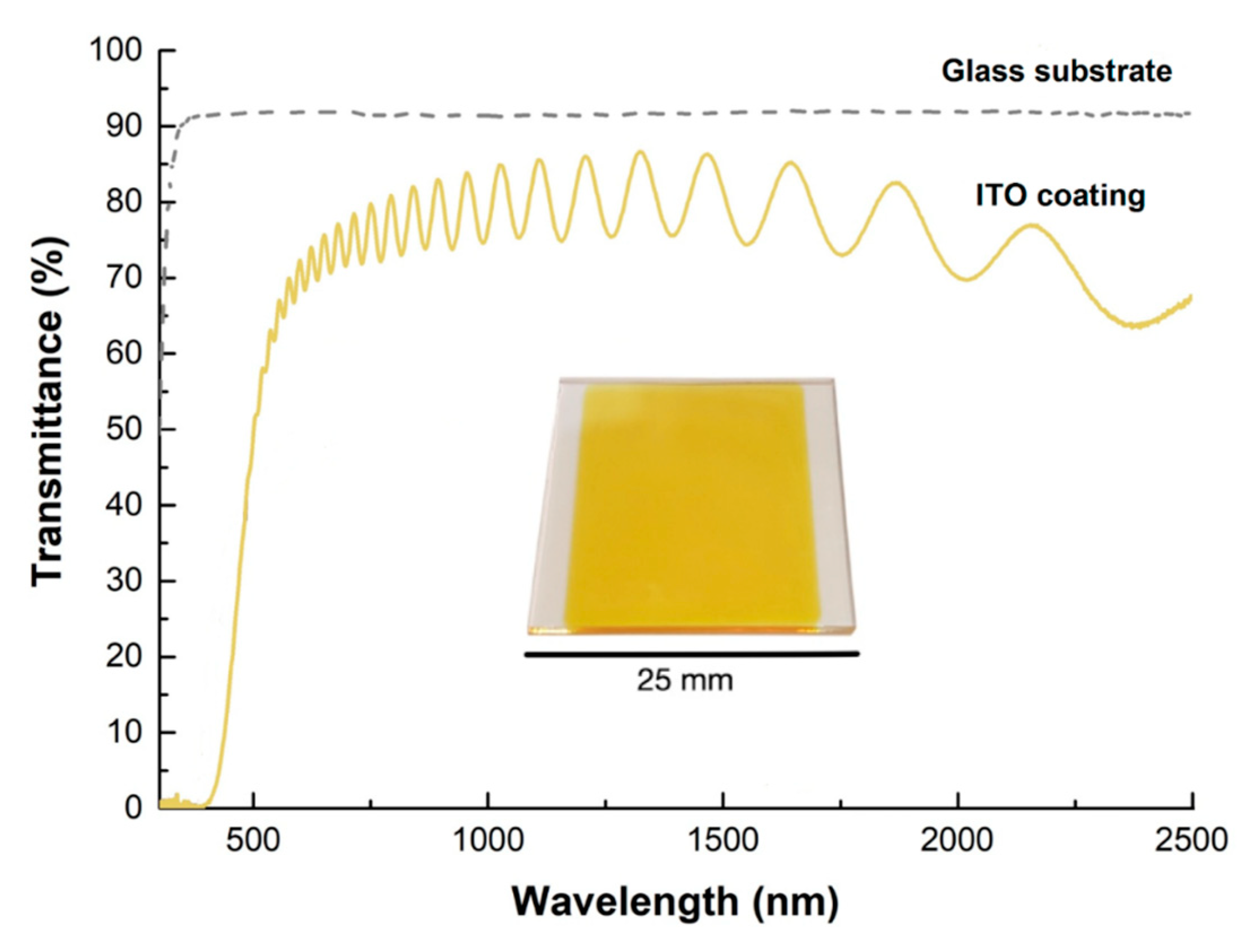
One critical parameter of ITO coatings is their optical transparency. The photograph in
Figure 3 shows a yellow (RGB = 226,205,101) colour for the ITO coating. As stated earlier, the oxygen content in ITO films is a critical parameter affecting both their transparency and conductivity. Higher oxygen concentrations result in fewer oxygen vacancies and highly resistive films. In this work, the resistivity of the coatings increased with the introduction of 1% O
2 during coating deposition to 1.3 × 10
−1 Ω·cm (from 5.29 × 10
−4 Ω·cm for coatings deposited in pure Ar; not shown here). Similar values have been reported for sputter-deposited ITO coatings in Ar and Ar/O
2 gas mixtures [
19,
25].
Figure 3 shows the transmittance of a thick ITO coating between 300 nm and 2500 nm, where an uncoated glass substrate is shown for comparison. The transmittance curve of the ITO coating shows ~60% at 550 nm. Transmittance values in ITO films are known to decrease with increasing thickness [
12,
13,
14,
23,
24], mainly due to absorption. For example, Kim et al. reported a drop in transmittance at 550 nm from ~85% to ~75% with an increase in the thickness from 100 to 1000 nm for ITO films deposited in an Ar/O
2 mixture [
12]. An optical bandgap of 2.9 eV was calculated using Tauc’s relation. This value is lower than the typically ~3.4–3.9 eV reported for ITO [
27]. Oxygen-deficient films, such as those reported here, have narrower bandgaps, resulting in a redshift of the optical transmittance spectrum [
19].
4. Conclusions
The structure and optical properties of ~3.3 μm thick ITO coatings deposited by radio frequency magnetron sputtering from a ceramic ITO target in an Ar/O2 gas mixture (total O2 flow of 1%) on unheated glass substrates was investigated. The coatings exhibit a (622) preferential orientation and a nanocrystalline structure and display good electrical resistivity, optical transmittance at 550 nm and optical band gap values of 1.3 × 10⁻¹ Ω·cm, ~60% and 2.9 eV, respectively.
This study has shown that micrometre thick ITO coatings with good performance can be synthesised by sputter deposition at low temperature. These initial results are expected to provide useful information and will help to guide future studies on the synthesis of high quality ITO coatings. For example, as protective coatings for facets in mirror-concentration systems to increase the service life of such mirrors under open atmospheric conditions and as thick epsilon-near-zero ITO metafilms for applications in optical communications, RF-photonics and integrated silicon photonics. The composition, structure and properties of such coatings can be tuned by adjusting the Ar/O2 gas mixture flow during deposition and/or by additional post-deposition treatments.
Author Contributions
Conceptualization: A.S., C.R., and A.M.; methodology: C.R., B.B., and E.B.; software: A.S.; validation: E.B. and M.A.B.; investigation: A.S., B.B., E.B., and S.J.H.; resources: A.M.; data curation: S.A.; writing—original draft preparation: A.S. and C.R.; writing—review and editing: E.B., M.A.B., and A.M.; visualization: A.S. and C.R.; supervision: C.R. and A.M.; project administration: A.M.; funding acquisition: A.M. All authors have read and agreed to the published version of the manuscript.
Funding
This research was funded by the European Research Council under the ERC Advanced Grant ‘IMPUNEP’, grant number 320879. The APC was funded by the University of Cyprus.
Acknowledgments
The authors are grateful to Pierre Couture and Jonathan England (UK National Ion Beam Centre, University of Surrey) for providing RBS measurements.
Conflicts of Interest
The authors declare no conflict of interest.
References
- Ellmer, K. Past achievements and future challenges in the development of optically transparent electrodes. Nat. Photonics 2012, 6, 809–817. [Google Scholar] [CrossRef]
- Granqvist, C.G. Transparent conductors as solar energy materials: A panoramic review. Sol. Energy Mater. Sol. Cells 2007, 91, 1529–1598. [Google Scholar] [CrossRef]
- Atabaev, I.G.; Khazhiev, M.U.; Zakirova, S.B.; Shermatov, Z. Correlation between the structure, specific resistance, and optical properties of ITO films grown by CVD. Appl. Sol. Energy (Engl. Transl. Geliotekhnika) 2017, 53, 322–325. [Google Scholar] [CrossRef]
- Maki, K.; Komiya, N.; Suzuki, A. Fabrication of thin films of ITO by aerosol CVD. Thin Solid Films 2003, 445, 224–228. [Google Scholar] [CrossRef]
- Senthilkumar, V.; Vickraman, P.; Jayachandran, M.; Sanjeeviraja, C. Structural and optical properties of indium tin oxide (ITO) thin films with different compositions prepared by electron beam evaporation. Vacuum 2010, 84, 864–869. [Google Scholar] [CrossRef]
- El-Nahass, M.M.; El-Menyawy, E.M. Thickness dependence of structural and optical properties of indium tin oxide nanofiber thin films prepared by electron beam evaporation onto quartz substrates. Mater. Sci. Eng. B Solid-State Mater. Adv. Technol. 2012, 177, 145–150. [Google Scholar] [CrossRef]
- Nuchuay, P.; Chaikeeree, T.; Horprathum, M.; Mungkung, N.; Kasayapanand, N.; Oros, C.; Limwichean, S.; Nuntawong, N.; Chananonnawathorn, C.; Patthanasettakul, V.; et al. Engineered omnidirectional antireflection ITO nanorod films with super hydrophobic surface via glancing-angle ion-assisted electron-beam evaporation deposition. Curr. Appl. Phys. 2017, 17, 222–229. [Google Scholar] [CrossRef]
- Biswas, N.; Ghosh, P.; Sarkar, S.; Moitra, D.; Biswas, P.K.; Jana, S.; Mukhopadhyay, A.K. Nanomechanical properties of dip coated indium tin oxide films on glass. Thin Solid Films 2015, 579, 21–29. [Google Scholar] [CrossRef]
- An, J.S.; Kim, S.C.; Hahn, S.H.; Ko, S.K.; Kim, E.J. Influence of annealing on the optical and the electrical properties of ITO thin films prepared by using a sol-gel spin method. J. Korean Phys. Soc. 2004, 45, 1629–1634. [Google Scholar]
- Zhang, L.; Lan, J.; Yang, J.; Guo, S.; Peng, J.; Zhang, L.; Tian, S.; Ju, S.; Xie, W. Study on the physical properties of indium tin oxide thin films deposited by microwave-assisted spray pyrolysis. J. Alloys Compd. 2017, 728, 1338–1345. [Google Scholar] [CrossRef]
- Kim, H.; Horwitz, J.S.; Kushto, G.; Piqué, A.; Kafafi, Z.H.; Gilmore, C.M.; Chrisey, D.B. Effect of film thickness on the properties of indium tin oxide thin films. J. Appl. Phys. 2000, 88, 6021–6025. [Google Scholar] [CrossRef]
- Kim, J.H.; Seong, T.Y.; Ahn, K.J.; Chung, K.B.; Seok, H.J.; Seo, H.J.; Kim, H.K. The effects of film thickness on the electrical, optical, and structural properties of cylindrical, rotating, magnetron-sputtered ITO films. Appl. Surf. Sci. 2018, 440, 1211–1218. [Google Scholar] [CrossRef]
- Eshaghi, A.; Graeli, A. Optical and electrical properties of indium tin oxide (ITO) nanostructured thin films deposited on polycarbonate substrates “thickness effect”. Optik 2014, 125, 1478–1481. [Google Scholar] [CrossRef]
- Hao, L.; Diao, X.; Xu, H.; Gu, B.; Wang, T. Thickness dependence of structural, electrical and optical properties of indium tin oxide (ITO) films deposited on PET substrates. Appl. Surf. Sci. 2008, 254, 3504–3508. [Google Scholar] [CrossRef]
- Sittinger, V.; Ruske, F.; Werner, W.; Jacobs, C.; Szyszka, B.; Christie, D.J. High power pulsed magnetron sputtering of transparent conducting oxides. Thin Solid Films 2008, 516, 5847–5859. [Google Scholar] [CrossRef]
- Jung, Y.S.; Lee, S.S. Development of indium tin oxide film texture during DC magnetron sputtering deposition. J. Cryst. Growth 2003, 259, 343–351. [Google Scholar] [CrossRef]
- Kurdesau, F.; Khripunov, G.; da Cunha, A.F.; Kaelin, M.; Tiwari, A.N. Comparative study of ITO layers deposited by DC and RF magnetron sputtering at room temperature. J. Non-Cryst. Solids 2006, 352, 1466–1470. [Google Scholar] [CrossRef]
- Qiao, Z.; Mergel, D. Comparison of radio-frequency and direct-current magnetron sputtered thin In2O3: Sn films. Thin Solid Films 2005, 484, 146–153. [Google Scholar] [CrossRef]
- Gorjanc, T.C.; Leong, D.; Py, C.; Roth, D. Room temperature deposition of ITO using r.f. magnetron sputtering. Thin Solid Films 2002, 413, 181–185. [Google Scholar] [CrossRef]
- Bhorde, A.; Jadhavar, A.; Waykar, R.; Nair, S.; Borate, H.; Pandharkar, S.; Aher, R.; Naik, D.; Vairale, P.; Lonkar, G.; et al. (400)-Oriented indium tin oxide thin films with high mobility and figure of merit prepared by radio frequency magnetron sputtering. Thin Solid Films 2020, 704, 137972. [Google Scholar] [CrossRef]
- Sousa, M.G.; da Cunha, A.F. Optimization of low temperature RF-magnetron sputtering of indium tin oxide films for solar cell applications. Appl. Surf. Sci. 2019, 484, 257–264. [Google Scholar] [CrossRef]
- Najwa, S.; Shuhaimi, A.; Talik, N.A.; Ameera, N.; Sobri, M.; Rusop, M. In-situ tuning of Sn doped In2O3 (ITO) films properties by controlling deposition Argon/Oxygen flow. Appl. Surf. Sci. 2019, 479, 1220–1225. [Google Scholar] [CrossRef]
- Amalathas, A.P.; Alkaisi, M.M. Effects of film thickness and sputtering power on properties of ITO thin films deposited by RF magnetron sputtering without oxygen. J. Mater. Sci. Mater. Electron. 2016, 27, 11064–11071. [Google Scholar] [CrossRef]
- Ghorannevis, Z.; Akbarnejad, E.; Ghoranneviss, M. Structural and morphological properties of ITO thin films grown by magnetron sputtering. J. Theor. Appl. Phys. 2015, 9, 285–290. [Google Scholar] [CrossRef] [Green Version]
- Kim, J.H.; Lee, J.H.; Heo, Y.W.; Kim, J.J.; Park, J.O. Effects of oxygen partial pressure on the preferential orientation and surface morphology of ITO films grown by RF magnetron sputtering. J. Electroceramics 2009, 23, 169–174. [Google Scholar] [CrossRef]
- Das, R.; Adhikary, K.; Ray, S. The role of oxygen and hydrogen partial pressures on structural and optical properties of ITO films deposited by reactive rf-magnetron sputtering. Appl. Surf. Sci. 2007, 253, 6068–6073. [Google Scholar] [CrossRef]
- Antony, A.; Nisha, M.; Manoj, R.; Jayaraj, M.K. Influence of target to substrate spacing on the properties of ITO thin films. Appl. Surf. Sci. 2004, 225, 294–301. [Google Scholar] [CrossRef]
- Hotovy, J.; Hüpkes, J.; Böttler, W.; Marins, E.; Spiess, L.; Kups, T.; Smirnov, V.; Hotovy, I.; Kováč, J. Sputtered ITO for application in thin-film silicon solar cells: Relationship between structural and electrical properties. Appl. Surf. Sci. 2013, 269, 81–87. [Google Scholar] [CrossRef]
- Lee, Y.-L.; Lee, K.-M. Effect of ambient gases on the characteristics of ITO thin films for OLEDs. Trans. Electr. Electron. Mater. 2009, 10, 203–207. [Google Scholar] [CrossRef] [Green Version]
- Ni, J.H.; Sarney, W.L.; Leff, A.C.; Cahill, J.P.; Zhou, W. Property variation in wavelength-thick epsilon-near-zero ITO metafilm for near IR photonic devices. Sci. Rep. 2020. [Google Scholar] [CrossRef]
- Polychronopoulou, K.; Rebholz, C.; Baker, M.A.; Theodorou, L.; Demas, N.G.; Hinder, S.J.; Polycarpou, A.A.; Doumanidis, C.C.; Böbel, K. Nanostructure, mechanical and tribological properties of reactive magnetron sputtered TiCx coatings. Diam. Relat. Mater. 2008, 17, 2054–2061. [Google Scholar] [CrossRef] [Green Version]
- Polychronopoulou, K.; Baker, M.A.; Rebholz, C.; Neidhardt, J.; O’Sullivan, M.; Reiter, A.E.; Kanakis, K.; Leyland, A.; Matthews, A.; Mitterer, C. The nanostructure, wear and corrosion performance of arc-evaporated CrBxNy nanocomposite coatings. Surf. Coat. Technol. 2009, 204, 246–255. [Google Scholar] [CrossRef] [Green Version]
- Rebholz, C.; Monclus, M.A.; Baker, M.A.; Mayrhofer, P.H.; Gibson, P.N.; Leyland, A.; Matthews, A. Hard and superhard TiAlBN coatings deposited by twin electron-beam evaporation. Surf. Coat. Technol. 2007, 201. [Google Scholar] [CrossRef]
- Gassenbauer, Y.; Schafranek, R.; Klein, A.; Zafeiratos, S.; Hävecker, M.; Knop-Gericke, A.; Schlögl, R. Surface states, surface potentials, and segregation at surfaces of tin-doped In2 O3. Phys. Rev. B Condens. Matter Mater. Phys. 2006, 73, 1–11. [Google Scholar] [CrossRef]
- Luo, S.; Kohiki, S.; Okada, K.; Shoji, F.; Shishido, T. Hydrogen effects on crystallinity, photoluminescence, and magnetization of indium tin oxide thin films sputter-deposited on glass substrate without heat treatment. Phys. Status Solidi Appl. Mater. Sci. 2010, 207, 386–390. [Google Scholar] [CrossRef] [Green Version]
| Publisher’s Note: MDPI stays neutral with regard to jurisdictional claims in published maps and institutional affiliations. |
© 2020 by the authors. Licensee MDPI, Basel, Switzerland. This article is an open access article distributed under the terms and conditions of the Creative Commons Attribution (CC BY) license (http://creativecommons.org/licenses/by/4.0/).


 and
and 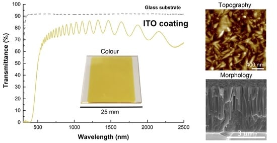