Article

Piezoelectric Hybrid Heterostructures PVDF/(Ba,Ca)(Zr,Ti)O3 Obtained by Laser Techniques

1
Plasma and Radiation Physics, National Institute for Lasers, 409 Atomistilor, 077125 Magurele, Romania
2
Faculty of Physics, University of Bucharest, 030018 Bucharest, Romania
*
Author to whom correspondence should be addressed.
Coatings 2020, 10(12), 1155; https://doi.org/10.3390/coatings10121155
Submission received: 2 November 2020 / Revised: 20 November 2020 / Accepted: 24 November 2020 / Published: 26 November 2020

Abstract

:
In this paper we report the development of thin films composed of two piezoelectric materials, namely (Ba(Ti0.8Zr0.2)O3-x(Ba0.7Ca0.3)TiO3 (BCTZ) and polyvinylidene difluoride (PVDF), thus obtaining high piezoelectric hybrid heterostructures for making them a viable option for wearable pressure sensors. The piezoelectric output response as a function of different weight percentage of BCTZ ceramic powders (x = 0.50 BCTZ50 and x = 0.55 BCTZ55) in the PVDF matrix was investigated. The highest value of the piezoelectric coefficient d33 and the capacitance, with low dielectric loss was obtained for the heterostructure composed of PVDF/BCTZ50.

1. Introduction

Piezoelectric materials play an important part in modern technologies currently. This type of material is used for electronic devices such as transducers that are used for microspeakers or for medical ultrasound, sensors used for measuring changes in temperature, pressure, strain or force and for motorized actuators among other applications. One of the most utilized piezoelectric materials are lead zirconate titanates Pb(ZrxTi1−x)O3 (PZT) and lanthanum modified lead zirconate titanate (Pb1−3x/2Lax)(ZryTi1−y)O3 (PLZT) due to their increased functional dielectric and ferroelectric properties [1,2,3]. PZT-based thin films have been used in different areas such as sensors, cantilever actuators [4,5] and ultrasonic micromotors [6]. For depositing PZT thin films various methods have been used both physical techniques such as reacting sputtering of multielement metallic targets [7] and rf magnetron sputtering [8], but also chemical methods such as metal-organic-decomposition (MOD) [9] and also laser deposition—pulsed laser deposition [10,11]. The drawbacks include the fact that the processes work with an excess of lead to compensate the lead loss before the perovskite formation or high temperature requirements for a self-stabilization of lead stoichiometry [4]. Moreover, their high acoustic impedance, lack of flexibility and brittleness limits their application field. The current legislation is based on restrictions on the use of materials with health and environmental risks and tends towards the use of lead-free materials for environmental protection. Lead containing materials are highly toxic and their toxicity is further enhanced at high temperatures due to the volatilization of the compounds. Piezoelectric materials that have in their composition lead were considered the only viable alternative to obtaining detection devices, such as pressure sensors.
Extensive studies are dedicated to the development of piezoelectric heterostructures combining both high piezoelectric activity, needed for energy harvesting or sensing applications—here piezoelectric ceramic materials such as PZT, PMN (lead-magnesiumniobate) and PMN-PT (lead-magnesiumniobate lead-titanate), with the flexibility and integration easiness of piezoelectric polymers (e.g., PVDF). In spite of the fact that the ceramic piezoelectric materials have, by far, superior piezoelectric properties, they are brittle, rigid and heavy, which means limited possibilities to integrate them into wearable smart devices [12,13]. On the other hand, the piezoelectric polymers do not match the piezoelectric activity of ceramic materials but they are flexible and lightweight, leading to the conclusion that a mix of ceramic material/polymer can solve the design problems for many practical applications.
To fulfill both superior functional piezoelectric properties and environmental regulations, the lead-free materials such as solid solutions based on barium titanate (BaTiO3) are mainly studied for piezoelectric functional properties to replace toxic lead-based titanium compounds (PbZrTiO3-PZT). From the point of view of the piezoelectric activity presented in the volumetric form, the solid solution with perovskite structure (Ba1−xCax)(ZryTi1−y)O3—(BCTZ) shows values of the piezoelectric coefficients similar or even higher PZT [14,15,16]. Scarisoreanu et al. obtained high values of dielectric permittivity (<3000), with low dielectric loss (<0.01) for BCTZ 45 thin films obtained by the pulsed laser deposition technique (PLD) [17]. Moreover, the author demonstrated that there is a complex dependence of the BCTZ thin film thickness to the dielectric and piezoelectric properties, with increased dielectric permittivity for the thinner deposited films due to the increased anisotropy [18].
The doping with Ca and Zr allows the flexibility to be obtained in stoichiometry, the tunability of functional properties through the variation of the level or the doping ratio being the main advantage. By incorporating BCTZ piezoelectric ceramic material into the polyvinylidene difluoride (PVDF) matrix, high piezoelectric and flexible heterostructures can be obtained. PVDF was chosen considering its excellent mechanical and electric properties making it a good candidate for a wide range of optical and magnetic applications, in the industrial and advanced sensor field [19,20,21]. In this regard, other studies were carried out in which the two compositions BCTZ and PVDF were used. PVDF polymer and BCTZ ceramic integration has been used in previous studies but by using different deposition methods, such as the sol–gel method through the citrate precursor method [22] and also using solid-state derived micron BCTZ in PVDF using dopamine as a surface functionalizer [23].
In this paper we demonstrated for the first time the development of flexible composite thin films based on BCTZ and PDVF deposited by laser deposition techniques (pulsed laser deposition and matrix assisted pulsed laser evaporation) with a high value of the piezoelectric coefficient d33 and the capacitance, and low dielectric losses. Using laser processing techniques (e.g., PLD and matrix assisted pulsed laser evaporation (MAPLE)), it is demonstrated here that is possible to integrate into a single structure both ceramic and polymer piezoelectric materials. The advantages of the laser processing approach is related to the fact that the multilayer heterostructures can be obtain without influencing the functional properties of the previous layer, as is occurring in sol–gel or other chemical routes [24,25]. Moreover, the functional property tunability as a function of BCTZ compositions has been pointed out. After our knowledge, there are no reports on this topic that use the present reported approach.

2. Materials and Methods

In order to obtain the PVDF/(Ba1−xCax)(ZryTi1−y)O3 thin films, two deposition methods were used, respectively pulsed laser deposition (PLD) and matrix assisted pulsed laser evaporation (MAPLE). After the obtaining process, the details of the obtaining procedure are given below, the samples were investigated by different techniques, followed by the integration into a testing device by depositing the necessary metallic electrodes for electrical measurements.
Thin films of BCTZ were deposited using the PLD technique in an interaction chamber equipped with a vacuum system, which can deliver pressures close to 10−7 mbar, a target rotation system and a xy motorized translation assembly were used to ensure a uniform ablation at the target level for increasing the uniformity of the deposited films. The substrate, in this case a Pt/Si was mounted on an oven, which was heated during deposition at Tdep = 700 °C to ensure better adherence of the deposited material onto the substrate. In this stage, two ceramic targets of BCTZ50 (50% BCT and 50% BZT) and BCTZ55 (55% BCT and 45% BZT), previously sintered at 1450 °C, were used for depositions. For irradiation of the target, an ArF excimer laser with 193 nm wavelength was used, the laser fluency was set at 2.1 J/cm2 and the films were deposited in the O2 atmosphere. The films were grown on Pt/Si substrates placed at a distance of 4 cm from the target.
Subsequently, a thin film of PVDF was deposited over the thin films that were thus obtained, using the matrix assisted pulsed laser evaporation technique (MAPLE). This method was chosen taking into consideration that the PVDF is a polymer sensible to high temperatures and this deposition technique allows the deposition of various materials (both organic and inorganic) without destroying the structure of the molecules and maintaining the stoichiometry of the deposited material [26]. In the case of thin films of PVDF, dimethylformamide (DMF) was used as a solvent. The mixture of DMF and PVDF, with a concentration of 9% PVDF was stirred at 50 °C for 30 min to yield a clear and homogenous solution, which was after poured into the target holder and subsequently frozen in liquid nitrogen. The target irradiation was done with a pulsed Nd:YAG laser, at a wavelength of 266 nm and a frequency of 10 Hz. All depositions were made at a pressure of 10−4 mbar, during the deposition process the target being maintained was cooled with liquid nitrogen (Ttarget = −180 °C).
Surface morphology and continuity analyses of the thin layers deposited were performed using the atomic force microscopy (AFM) technique (model XE100, Park Systems, Suwon, Korea) and scanning electron microscopy (JSM-531 Inspect S Electron Scanning Microscope, FEI Company, Prague, Czech Republic). The AFM was equipped with a 200× magnification camera microscope, which allowed good sample viewing and positioning.
The Fourier-transform infrared spectroscopy (FTIR) measurements were made with the Jasco FTIR 6300 spectrometer (Jasco, Pfungstadt, Germany), in the ATR mode and with a resolution of 4 cm−1.
The thin films thus deposited were also measured using the PiezoMeter System PM300 from the Piezotest Pte. Ltd. (London, UK) device to highlight parameters such as d33, dielectric capacity and dielectric loss. The device works by clamping the probe and subjecting it to a low frequency force. For calculating the d33 coefficient PFM switching spectroscopy determinations were performed to evaluate the piezoelectric behavior of the deposited materials, using the existing AFM system.
Moreover, optical measurements were conducted using a Woollam Variable Angle Spectroscopic Ellipsometer (VASE, J.A. WOOLLAM CO., INC, Lincoln, NE, USA) system that comes with a high pressure Xe discharge lamp incorporated in an HS-190 monochromator. The light beam incidence angle was set to 60–70°, with a step of 5°.

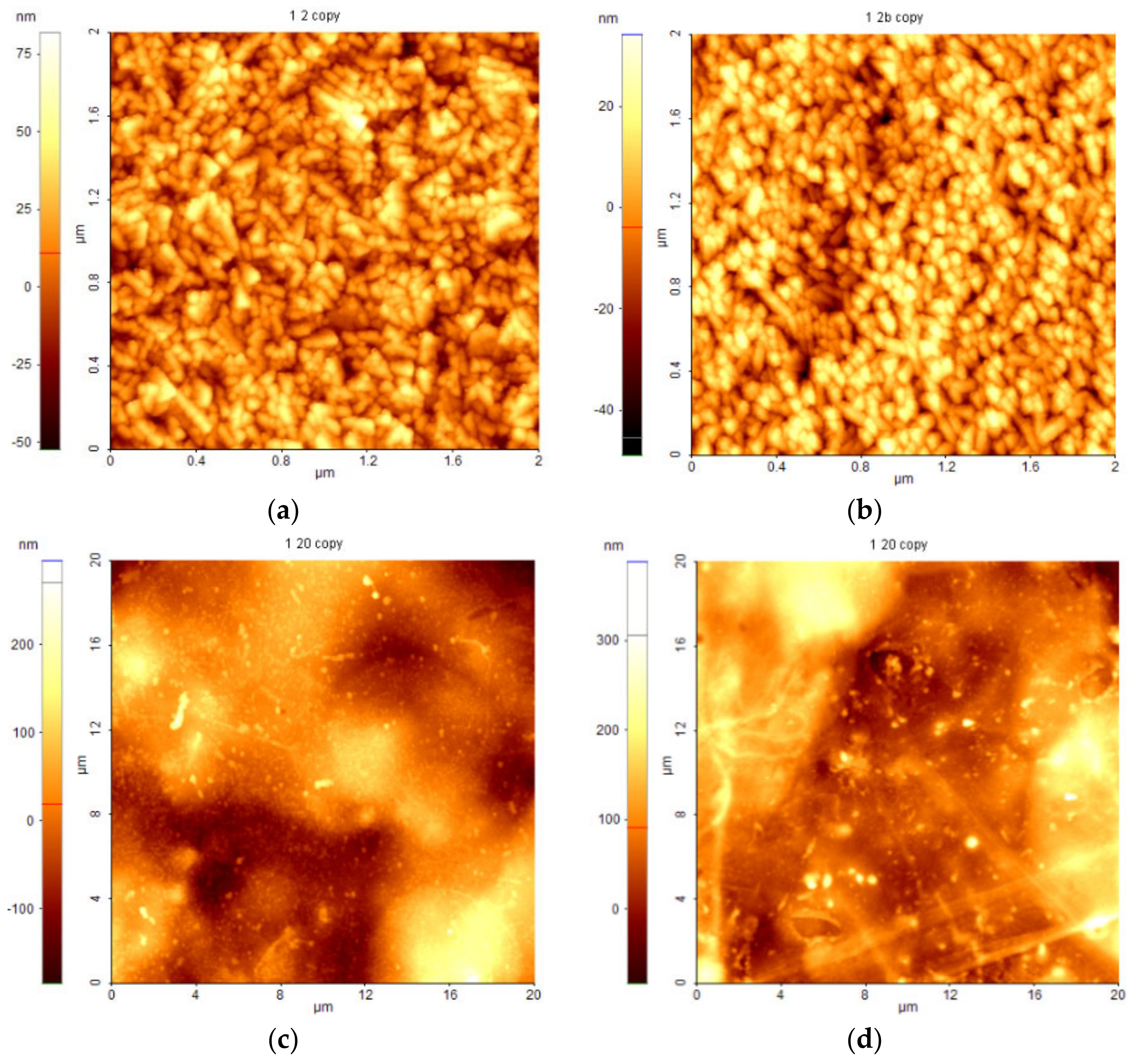
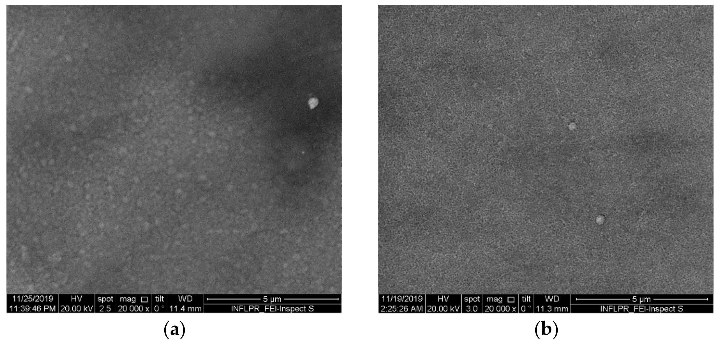
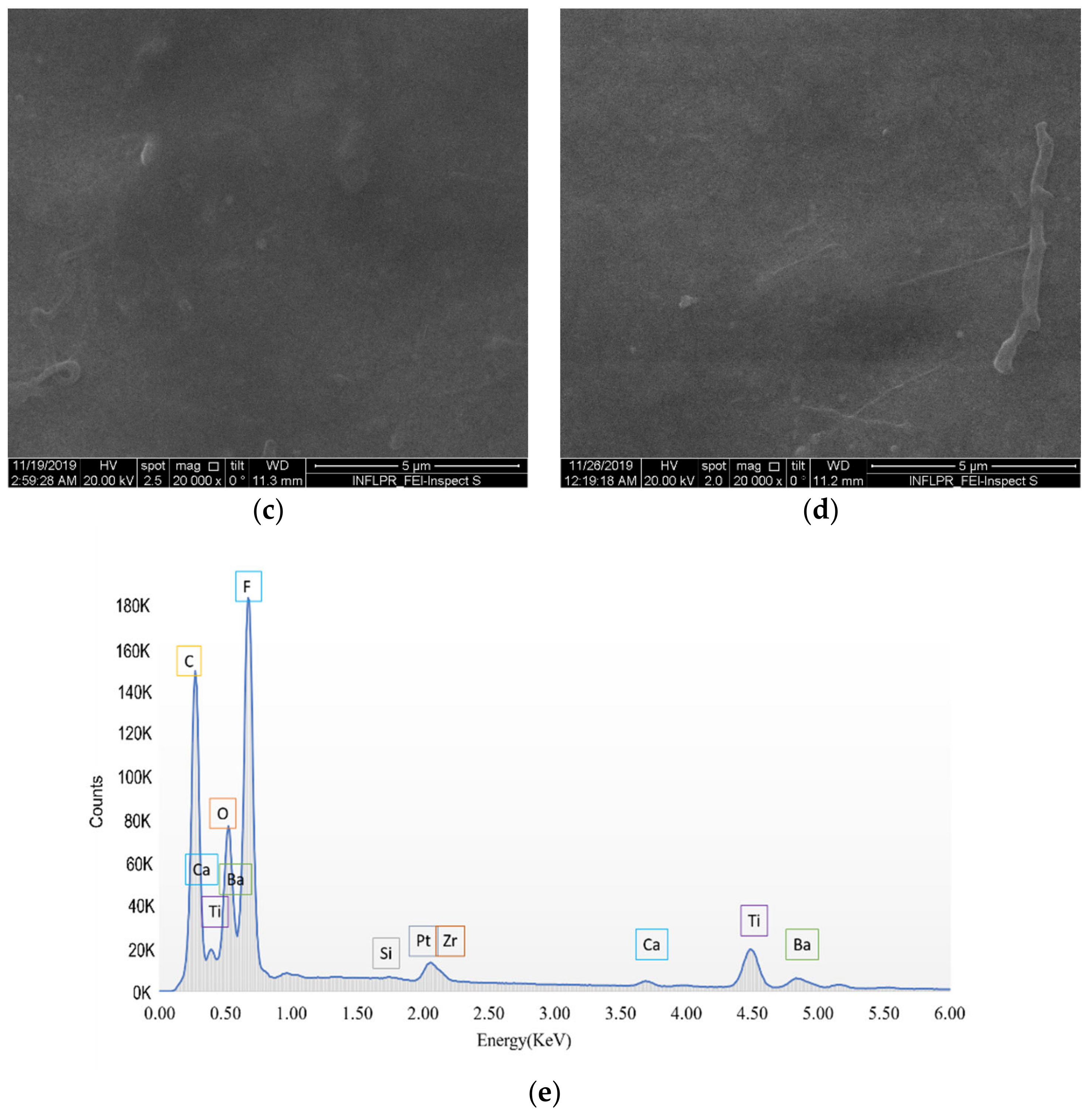
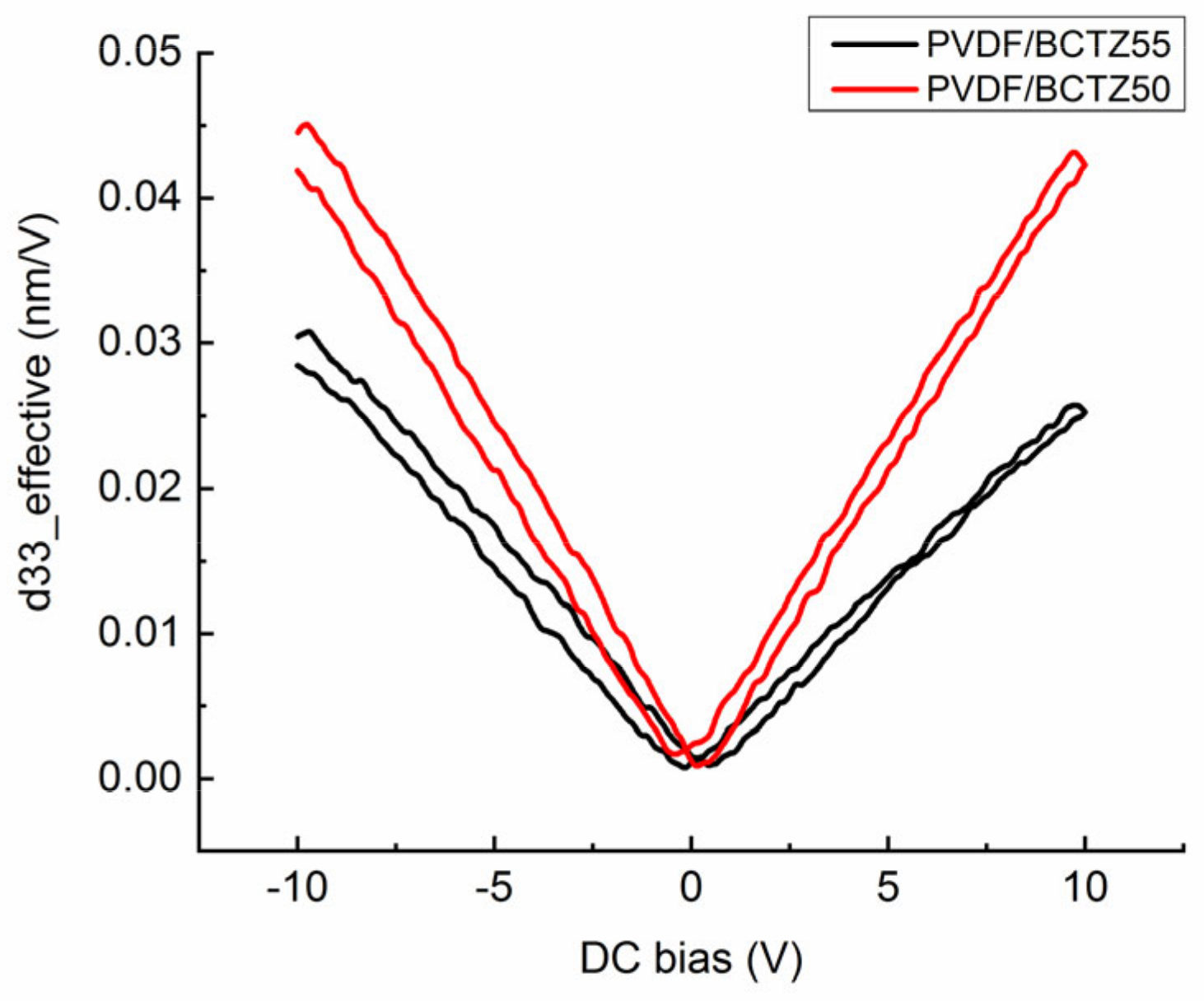
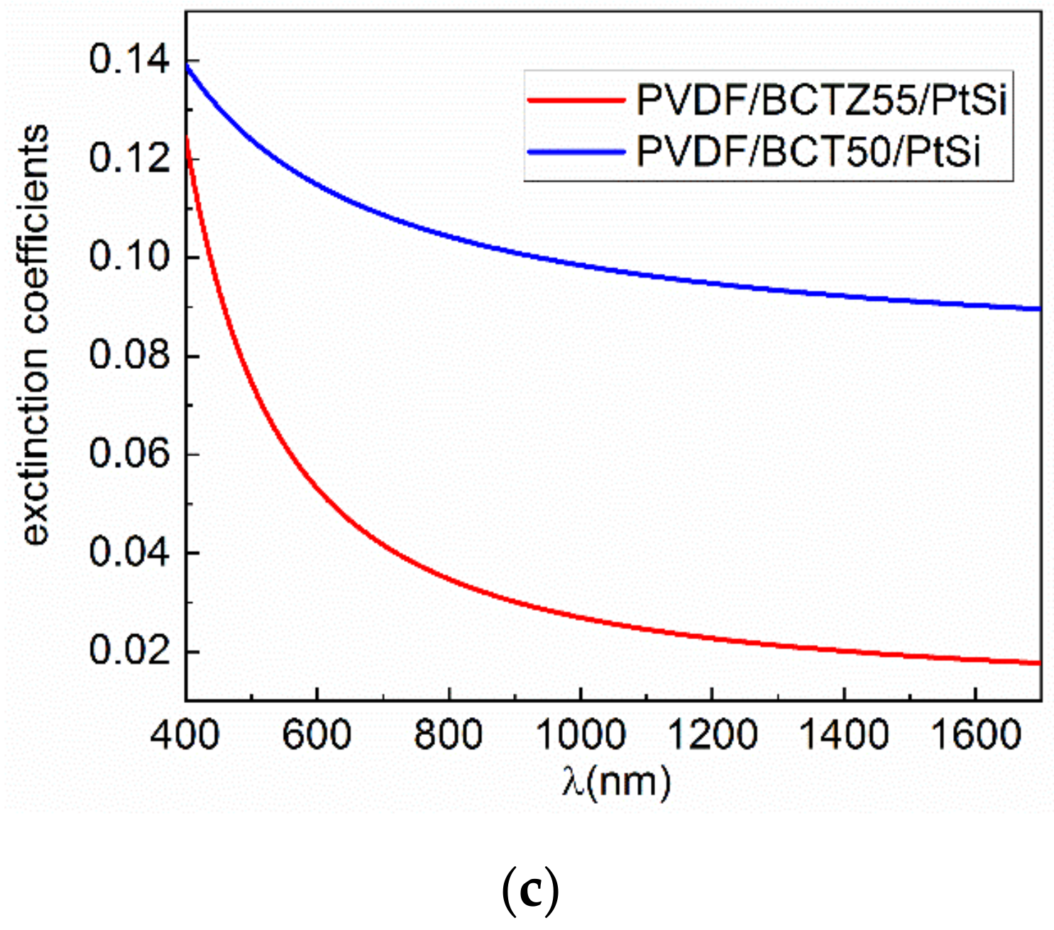
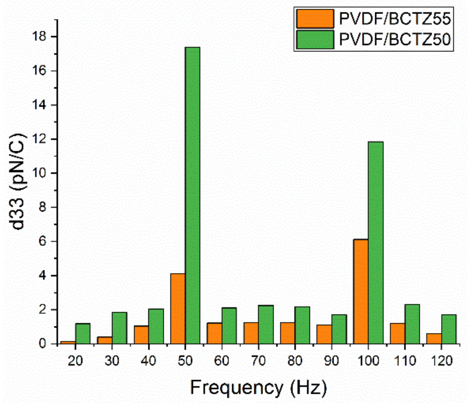
3. Results and Discussion

The morphology of the deposited samples was characterized using scanning electron microscopy (SEM) and atomic force microscopy (AFM). AFM measurements (XE100, Park Systems, Suwon, Korea) in the non-contact mode were performed to quantitatively analyze the films roughness parameters. SEM investigations were carried out using a scanning electron microscope at accelerating voltages between 5 and 25 kV. The chemical evaluation of the samples was performed using energy dispersive X-ray spectroscopy with 10 kV accelerating voltage (EDAX, Element 2CB detector on a JSM-531 Inspect S Electron Scanning Microscope, FEI Company, Hillsborough, OR, USA).
The morphology of the BCTZ samples grown on Pt/Si, obtained in the same conditions (pressure of 0.1 mbar O2, temperature of 700 °C, distance from the target of 4 cm and laser fluence of 2.1 J/cm2) shows that the deposited thin films did not present major defects or cracks and were rather smooth (Figure 1).
Details about the morphological film characteristics were also revealed by SEM images (Figure 2). In order to avoid the deterioration of the analyzed material by the prolonged exposure to the electron beam, the imaging analyzes were performed at low acceleration voltages, 2–10 kV, small sample currents, 0.10–0.50 nA, using the scanning approach based on intersecting lines, scanning, integration of scanning frames and automatic correction of electrostatic drift.
The images obtained by the scanning electron microscopy technique (Figure 2) revealed that the PVDF coatings obtained by MAPLE present a morphology characterized by a high density of circular and elongated formations, randomly distributed on the surface of the films, but covering the entire surface, in accordance with previous reports [16]. The surface morphology revealed strong dependence of the BCTZ film roughness.
Figure 2-insert depicts the EDAX spectrum of the deposited thin film. The elemental compositions of the deposited coatings unveiled carbon, fluorine and oxygen as the main chemical elements originating from the PVDF structure. The peaks of Si and Pt from the EDS spectrum (Figure 2e) are characteristics of the substrate used for deposition and those of Ba, Ca, Ti and Zr were characteristics of the layer of BCTZ deposited by PLD. The data were obtained from three different locations on each surface and showed that all of the coatings were uniform formed on the substrate.
In order to determine the chemical composition and the presence or absence of contaminants or defects in the PVDF samples after deposition, using the MAPLE technique, FT-IR microscopy analyzes were performed. Initial and final solutions and films were deposited for two different thicknesses and subsequently analyzed (Figure 3).
Out of the five crystal phases of PVDF, the α and β phases are the most common [27]. In the α phase, PVDF is more stable, but it becomes paraelectric and it cannot be used as a ferroelectric thin film [28]. Taking this into consideration, obtaining PVDF in the β phase was an important factor for obtaining highly responsive piezoelectric thin films. This analysis demonstrates that the chemical imprint of PVDF is retained after deposition. By increasing fluency in the sample, the PVDF material has a lower IR signal, which means that the chemical bonds of the material tend to be broken. Thus, maintaining a lower fluency increases the relative amount of β phases.
PFM switching spectroscopy determinations were performed to evaluate the piezoelectric behavior of the deposited materials. Two potentials were applied as follows: on the conductive AFM tip, in contact with the material, a potential of 3 V, 17 kHz AC was applied and on the Pt/Si substrate a DC potential was applied. The range of the scanned voltage was as follows: −10 V... + 10 V... – 10 V. The amplitude and PFM phase were recorded according to the DC potential applied, at two points on each sample (Figure 4).
From the amplitude of the response the d33 coefficient was calculated effectively. In Figure 5 are presented its values, obtained by averaging the two measurements on each sample.
It is observed that the amplitude of the PFM signal has a linear behavior in relation to the applied electric field, but it does not saturate. This may be due to the fact that the thickness of the samples does not allow reaching a sufficiently strong electric field, at the voltage of ±10 V, for the saturation.
The optical properties of the PVDF/BCTZ heterostructures deposited on Pt/Si substrates were determined by spectroscopic ellipsometry technique using a Woollam V-Vase ellipsometer (Quantum Design GmbH, Darmstadt, Germany). The experimental measurements were done in the 400–1700 nm range of wavelength with a step of 2 nm at 60–70° angles of incidence. Ellipsometry is a comparative technique, which is why, for extracting the optical constants and values of thin film thickness an optical model is required.
In our case the optical model consisted of a stack of 5 layers as follows the silicon substrate, the Pt layer with a thickness of 150 nm, the BCTZ and PVDF layers and the top rough layer. Since the thickness of Pt layer is high enough, this layer can be considered as a substrate and the optical constants was taken from the literature [29]. For the BCTZ layer, a simple Cauchy dispersion function was used to calculate values of optical constants. For the PVDF component, the Cauchy dispersion with the Urbach tail model was used to fit the experimental data. Instead, for the top rough layer a B-EMA approximation [30,31] was used meaning that this layer was considered to be composed by 50% air and 50% PVDF.
The BCTZ layers were measured before PVDF deposition and the optical constants of this layer were calculated. The BCTZ thin films was found to be optical transparent (k = 0 where “k” is the extinction coefficient) in the range of 400–1700 nm, for both compositions. This behavior is expected for the BCTZ thin films, taking into account the optical band gap value of this material of around 3.90 eV (317 nm) [32]. Figure 6 shows the dispersion of the refractive index for both compositions of BCTZ.
The values of the refractive index were lower than reported values for the epitaxial thin film of BCZT (n~2.4, where “n” is the refractive index), but are comparable with values reported in literature for polycrystalline thin films growth on PtSi (n~2.2-BCTZ50) [33]. The same results were found for PVDF layers, all optical constants are comparable with the literature [32,33]. The obtained values of the refractive index n~1.44–1.46 are similar with those reported by Vhun et al. for the β-PVDF [34], while the extinction coefficients have a non-zero values (k~0.02–0.12) on the whole range of measured wavelength [35].
The calculated thickness values were around d~450–460 nm (where “d” is the thickness of layer) for the BCTZ deposited by PLD, while for PVDF deposited by MAPLE were in the range of 220–250 nm. From the table below (Table 1) it can be observed that the BCTZ 50 films have a slightly higher thickness and roughness than those of BCTZ 55.
Films submitted were also measured using the Piezotest device to highlight parameters such as d33, dielectric capacity and loss. The method is used to make measurements on different types of materials such as piezo-ceramics, polymers, thin films and crystalline materials. The system works by fixing the sample and subjecting it to a low frequency force. The processing of the electrical signals from the thin film, in this case, and the comparison with a built-in reference, allows the system to read directly d33. In order to measure these parameters, on the thin films were deposited electrodes of gold using the evaporation method under 10−5 vacuum. For a better adhesion of the gold, a chromium 5 nm layer was first deposited, followed by a 200 nm gold on top of it [36]. The electrical contact between the surface electrode and the Pt/Si contact electrode was done using conductive silver paint [37]. The piezoelectric measurements were done at a frequency between 10 and 120 Hz, a dynamic force of 0.05 N and a static force of 10 N.
The highest value of the piezoelectric coefficient d33 and the electrical capacity, in the conditions of low dielectric losses was obtained in the case of sample PVDF/BCTZ50, as can be seen from the graph below and from Table 2.
Both samples had a piezoelectric response starting with a frequency as low as 20 Hz and both exhibited two peak responses at 50 and at 100 Hz, as it can be observed in Figure 7. The sample of PVDF/BCTZ50 had a response of more than 4 times higher than the one of PVDF/BCTZ55 at 50 Hz and 2 times higher for 100 Hz. Nevertheless, if we compare responses of the same sample at different frequencies, we note that PVDF/BCTZ50 has a higher response at 50 Hz, but PVDF/BCTZ55 responds better at 100 Hz. This can also be explained using the phase diagram of the two ceramics, called morphotropic phase boundaries (MPBs), situated between tetragonal/rhombohedral ferroelectric phases—where the intrinsic functional properties are maximized [38,39]. The obtained values for the heterostructure composed of PVDF and BCTZ are higher than the ones reported until now by Kalkur et al. [40]. The qualitative differences—as the measuring system Piezotest is more suitable for more thicker samples—between heterostructures containing BCTZ55 and BCTZ 50 compositions are high, PVDF/BCTZ50 showing a high d33 value and impressive dielectric permittivity while the PVDF/BCTZ55 heterostructure has very low dielectric losses (tan δ ≈ 0.0006, where “tan δ” is the dielectric loss tangent). The same behavior can be seen for bulk BCTZ compositions, the functional property tunability of these solid solutions being the main advantage [41].

4. Conclusions

Polycrystalline thin films composed of two piezoelectric materials (Ba(Ti0.8Zr0.2)O3-x(Ba0.7Ca0.3)TiO3 (BCTZ) and polyvinylidene difluoride (PVDF) have been deposited on Pt/Si substrates using two laser deposition methods: pulsed laser deposition for the BCTZ and matrix assisted pulsed laser evaporation for the polymer PVDF. For the pulsed laser deposition two different weight percentages of BCTZ ceramic powders (x = 0.50 BCTZ50 and x = 0.55 BCTZ55) was used. The morphological analysis of the thin films revealed a surface characterized by a high density of circular and elongated formations, randomly distributed and covering the entire substrate subjected to the deposition. The FTIR analysis demonstrated the presence of numerous β phases in the composition of PVDF after being deposited by the MAPLE technique. EDS analysis proved that there were no contaminants in the obtained heterostructures. The optical properties of the thin films deposited on Pt/Si substrates were determined by the spectroscopic ellipsometry technique for both the BCTZ thin films and the PVDF/BCTZ heterostructures demonstrating that the values of the refractive index were comparable with values reported in literature. The values of d33 effective coefficient were investigated using PFM and Piezotest device. The amplitude of the PFM signal had a linear behavior in relation to the applied electric field. Moreover, the Piezotest results demonstrated high values of the capacitance and low dielectric loss for the PVDF/BCTZ50 heterostructures. The tunability of the dielectric and piezoelectric properties of PVDF/BCTZ heterostructures as a function of used BCTZ compositions has been also evidenced, making them more addressable to practical applications.

Author Contributions

N.D.S. and N.E. conceived, designed the experiments, N.D.S., V.I., and N.E. cowrote the paper, N.E. performed the PLD and MAPLE deposition, V.I. conducted the optical analysis, A.B. and A.M. performed the SEM, AFM and PFM and N.E. performed Piezotest measurements. All authors have read and agreed to the published version of the manuscript.

Funding

This work was supported by a grant of the Romanian Ministry of Research and Innovation, PCCDI—UEFISCDI, project number PN-III-P1-1.2-PCCDI-2017-0172/15PCCDI within PNCDI III and by the National Authority for Research and Innovation in the frame of the Nucleus Program.

Conflicts of Interest

The authors declare no conflict of interest.

References

  1. Jaffe, B.; Roth, R.S.; Marzullo, S. Piezoelectric properties of lead zirconate-lead titanate solid-solution ceramics. J. Appl. Phys. 1954, 25, 809–810. [Google Scholar] [CrossRef]
  2. Yamamoto, T. Ferroelectric properties of the PbZrO3–PbTiO3 system. Jpn. J. Appl. Phys. 1996, 35, 5104–5108. [Google Scholar] [CrossRef]
  3. Georges, R. Characterization of PLZT ceramics for optical sensor and actuator devices. In Ceramic Materials—Progress in Modern Ceramics; IntechOpen: London, UK, 2012. [Google Scholar]
  4. Muralt, P. PZT thin films for microsensors and actuators: Where do we stand? IEEE Trans. Ultrason. Ferroelectr. Freq. Control. 2000, 47, 903–915. [Google Scholar] [CrossRef]
  5. Kim, H.; In, C.; Yoon, G.; Kim, J. Design and fabrication of a micro PZT cantilever array actuator for applications in fluidic systems. J. Mech. Sci. Technol. 2005, 19, 1544–1553. [Google Scholar] [CrossRef]
  6. Kueppers, H.; Hoffmann, M.; Leuerer, T.; Schneller, T.; Boettger, U.; Waser, R.; Mokwa, W.; Schnakenberg, U. Basic investigations on a piezoelectric bending actuator for micro-electro-mechanical applications. Integr. Ferroelectr. 2001, 35, 269–281. [Google Scholar] [CrossRef]
  7. Sreenivas, K.; Sayer, M. Characterization of Pb(Zr,Ti)O3 thin films deposited from multielement metal targets. J. Appl. Phys. 1988, 64, 1484–1493. [Google Scholar] [CrossRef]
  8. Krupanidhi, S.B.; Maffei, N.; Sayer, M.; El-Assal, K. rf planar magnetron sputtering and characterization of ferroelectric Pb(Zr,Ti)O3 films. J. Appl. Phys. 1983, 54, 6601. [Google Scholar] [CrossRef]
  9. Spierings, G.A.C.M.; Ulenaers, M.J.E.; Kampschöer, G.L.M.; Van Hal, H.A.M.; Larsen, P.K. Preparation and ferroelectric properties of PbZr0.53Ti0.47O3 thin films by spin coating and metalorganic decomposition. J. Appl. Phys. 1991, 70, 2290–2298. [Google Scholar] [CrossRef]
  10. Verardi, P.; Dinescu, M.; Craciun, F. Pulsed laser deposition and characterization of PZT thin films. Appl. Surf. Sci. 2000, 154, 514–518. [Google Scholar] [CrossRef]
  11. Roy, D.; Krupanidhi, S.B.; Dougherty, J.P. Excimer laser ablated lead zirconate titanate thin films. J. Appl. Phys. 1991, 69, 7930–7932. [Google Scholar] [CrossRef]
  12. Qin, Y.; Wang, X.; Wang, Z.L. Erratum: Microfibre–nanowire hybrid structure for energy scavenging. Nat. Cell Biol. 2009, 457, 340. [Google Scholar] [CrossRef] [Green Version]
  13. Shenck, N.S.; Paradiso, J.A. Energy scavenging with shoe-mounted piezoelectrics. IEEE Micro 2001, 21, 30–42. [Google Scholar] [CrossRef]
  14. Xue, D.; Zhou, Y.; Bao, H.; Zhou, C.; Gao, J.; Ren, X. Elastic, piezoelectric, and dielectric properties of Ba(Zr0.2Ti0.8)O3-50(Ba0.7Ca0.3)TiO3 Pb-free ceramic at the morphotropic phase boundary. J. Appl. Phys. 2011, 109, 054110. [Google Scholar] [CrossRef] [Green Version]
  15. Dezhen, X.; Yumei, Z.; Huixin, B.; Jinghui, G.; Chao, Z.; Xiaobing, R. Large piezoelectric effect in Pb-free Ba(Ti,Sn)O3x(Ba,Ca)TiO3 ceramics. Appl. Phys. Lett. 2011, 99, 122901. [Google Scholar] [CrossRef]
  16. Scarisoreanu, N.D.; Craciun, F.; Ion, V.; Birjega, R.; Bercea, A.; Dinca, V.; Dinescu, M.; Sima, L.E.; Icriverzi, M.; Roseanu, A.; et al. Lead-free piezoelectric (Ba,Ca)(Zr,Ti)O3 thin films for biocompatible and flexible devices. ACS Appl. Mater. Interfaces 2016, 9, 266–278. [Google Scholar] [CrossRef]
  17. Scarisoreanu, N.D.; Craciun, F.; Moldovan, A.; Ion, V.; Birjega, R.; Ghica, C.; Negrea, R.F.; Dinescu, M. High permittivity (1−x)Ba(Zr0.2Ti0.8)O3x(Ba0.7Ca0.3)TiO3 (x = 0.45) epitaxial thin films with nanoscale phase fluctuations. ACS Appl. Mater. Interfaces 2015, 7, 23984–23992. [Google Scholar] [CrossRef] [Green Version]
  18. Ion, V.; Craciun, F.; Scarisoreanu, N.D.; Moldovan, A.; Andrei, A.; Birjega, R.; Ghica, C.; Di Pietrantonio, F.; Cannata, D.; Benetti, M.; et al. Impact of thickness variation on structural, dielectric and piezoelectric properties of (Ba,Ca)(Ti,Zr)O3 epitaxial thin films. Sci. Rep. 2018, 8, 1–9. [Google Scholar] [CrossRef] [Green Version]
  19. Li, S.; Lin, M.M.; Toprak, M.S.; Kim, D.K.; Muhammed, M. Nanocomposites of polymer and inorganic nanoparticles for optical and magnetic applications. Nano Rev. 2010, 1. [Google Scholar] [CrossRef] [PubMed]
  20. Baumgärtel, K.H.; Zöllner, D.; Krieger, K.-L. Classification and Simulation Method for Piezoelectric PVDF Sensors. Proc. Technol. 2016, 26, 491–498. [Google Scholar] [CrossRef] [Green Version]
  21. Kim, H.; Fernando, T.; Li, M.; Lin, Y.; Tseng, T.-L.B. Fabrication and characterization of 3D printed BaTiO3/PVDF nanocomposites. J. Compos. Mater. 2018, 52, 197–206. [Google Scholar] [CrossRef] [Green Version]
  22. Sadhu, S.P.P.; Siddabattuni, S.; Varma, K.B.R. Enhanced dielectric properties and energy storage density of surface engineered BCZT/PVDF-HFP nanodielectrics. J. Mater. Sci. Mater. Electron. 2018, 29, 6174–6182. [Google Scholar] [CrossRef]
  23. Luo, B.; Wang, X.; Wang, Y.; Li, L. Fabrication, characterization, properties and theoretical analysis of ceramic/PVDF composite flexible films with high dielectric constant and low dielectric loss. J. Mater. Chem. A 2014, 2, 510–519. [Google Scholar] [CrossRef]
  24. Itina, T. Laser Ablation—From Fundamentals to Applications; Croatia InTech: Rijeka, Croatia, 2017; ISBN 978-953-51-3700-9. [Google Scholar]
  25. Caricato, A.P.; Luches, A. Applications of the matrix-assisted pulsed laser evaporation method for the deposition of organic, biological and nanoparticle thin films: A review. Appl. Phys. A 2011, 105, 565–582. [Google Scholar] [CrossRef]
  26. Piqué, A.; Wu, P.; Ringeisen, B.R.; Bubb, D.; Melinger, J.S.; McGill, R.; Chrisey, D. Processing of functional polymers and organic thin films by the matrix-assisted pulsed laser evaporation (MAPLE) technique. Appl. Surf. Sci. 2002, 186, 408–415. [Google Scholar] [CrossRef]
  27. Leonard, C.; Halary, J.L.; Monnerie, L. Crystallization of poly(vinylidene fluoride)-poly(methyl methacrylate) blends: Analysis of the molecular parameters controlling the nature of poly(vinylidene fluoride) crystalline phase. Macromolecules 1988, 21, 2988–2994. [Google Scholar] [CrossRef]
  28. Li, M.; Stingelin, N.; Michels, J.J.; Spijkman, M.-J.; Asadi, K.; Feldman, K.; Blom, P.W.M.; De Leeuw, D.M. Ferroelectric phase diagram of PVDF:PMMA. Macromolecules 2012, 45, 7477–7485. [Google Scholar] [CrossRef] [Green Version]
  29. Palik, E. Handbook of Optical Constants of Solids; Elsevier BV: Amsterdam, The Netherlands, 1985; Volume 1. [Google Scholar]
  30. Fujiwara, H. Spectroscopic Ellipsometry Principles and Applications; John Wiley & Sons Ltd.: Hoboken, NJ, USA, 2007; ISBN 978-0-470-01608-4. [Google Scholar]
  31. Harland, G.; Hilfiker, J.N. Spectroscopic Ellipsometry- Practical Application to Thin Film Characterization; Momentum Press Enginneering: New York, NJ, USA, 2016. [Google Scholar]
  32. Lin, Y.; Wu, G.; Qin, N.; Bao, D. Structure, dielectric, ferroelectric, and optical properties of (1−x)Ba(Zr0.2Ti0.8)O3x(Ba0.7Ca0.3)TiO3 thin films prepared by sol–gel method. Thin Solid Films 2012, 520, 2800–2804. [Google Scholar] [CrossRef]
  33. Wang, H.; Xu, J.; Zhao, P.; Ma, C.; Wang, L.; Bian, L.; Chang, A. Optical character of barium titanate based thin films around the phase transition. Ferroelectrics 2016, 491, 8–14. [Google Scholar] [CrossRef]
  34. Duan, C.-G.; Mei, W.N.; Yin, W.G.; Liu, J.; Hardy, J.R.; Bai, M.; Ducharme, S. Theoretical study on the optical properties of polyvinylidene fluoride crystal. J. Phys. Condens. Matter 2003, 15, 3805–3811. [Google Scholar] [CrossRef] [Green Version]
  35. Ismail, A.; Mohammed, M.; Fouad, S. Optical and structural properties of polyvinylidene fluoride (PVDF)/reduced graphene oxide (RGO) nanocomposites. J. Mol. Struct. 2018, 1170, 51–59. [Google Scholar] [CrossRef]
  36. The Vacuum Deposition of Gold. Available online: https://link.springer.com/journal/13404/volumes-and-issues/4-2 (accessed on 10 October 2020).
  37. Southin, J.E.A.; Wilson, S.A.; Schmitt, D.; Whatmore, R.W. e31,f determination for PZT films using a conventional ‘d33′ meter. J. Phys. D Appl. Phys. 2001, 34, 1456–1460. [Google Scholar] [CrossRef]
  38. Gao, J.; Xue, D.; Wang, Y.; Wang, D.; Zhang, L.; Wu, H.; Guo, S.; Bao, H.; Zhou, C.; Liu, W.; et al. Microstructure basis for strong piezoelectricity in Pb-free Ba(Zr0.2Ti0.8)O3-(Ba0.7Ca0.3)TiO3 ceramics. Appl. Phys. Lett. 2011, 99, 092901. [Google Scholar] [CrossRef]
  39. Cordero, F.; Craciun, F.; Dinescu, M.; Scarisoreanu, N.D.; Galassi, C.; Schranz, W.; Soprunyuk, V.P. Elastic response of (1–x)Ba(Ti0.8Zr0.2)O3x(Ba0.7Ca0.3)TiO3 (x = 0.45–0.55) and the role of the intermediate orthorhombic phase in enhancing the piezoelectric coupling. Appl. Phys. Lett. 2014, 105, 232904. [Google Scholar] [CrossRef]
  40. Kalkur, T.S.; Yi, W.-C.; Philofsky, E.; Kammerdiner, L.; Rywak, T. Electrical characteristics of high dielectric constant BCTZ thin films. Integr. Ferroelectr. 2001, 38, 289–295. [Google Scholar] [CrossRef]
  41. Bao, H.; Zhou, C.; Xue, D.; Gao, J.; Ren, X. A modified lead-free piezoelectric BZT–xBCT system with higher TC. J. Phys. D Appl. Phys. 2010, 43, 465401. [Google Scholar] [CrossRef]
Figure 1. Atomic force microscopy (AFM) images for BCTZ thin films deposited by pulsed laser deposition (PLD) on (Pt/Si) heated at 700 °C in 0.1 mbar of oxygen; (a) BCTZ55 with RMS = 16.9 nm; (b) BCTZ50 with = RMS 10.7 nm; (c) PVDF 9% + DMF/BCTZ55/PtSi with RMS = 71.2 nm and (d) PVDF 9% + DMF/BCTZ50/PtSi with RMS = 59.3 nm
Coatings 10 01155 g001
Figure 2. SEM images for BCTZ thin films deposited by PLD on (Pt/Si) heated at 700 °C in 0.1 mbar of oxygen; (a) BCTZ55 with RMS = 23.28 nm; (b) BCTZ50 with = RMS 44.11nm; (c) PVDF 9% + DMF/BCTZ55/PtSi; (d) PVDF 9% + DMF/BCTZ50/PtSi and (e) EDAX spectrum of PVDF 9% + DMF/BCTZ55/PtSi.
Coatings 10 01155 g002aCoatings 10 01155 g002b
Figure 3. FTIR spectra for PVDF/DMF solutions.
Coatings 10 01155 g003
Figure 4. Phase (a) and amplitude (b) of the piezoelectric response for the samples of BCTZ 55/Pt/Si and BCTZ 50 Pt/Si.
Coatings 10 01155 g004
Figure 5. The value of the d33 effective coefficient for the samples of BCTZ 55/Pt/Si and BCTZ 50 Pt/Si.
Coatings 10 01155 g005
Figure 6. Optical constants dispersion curves obtained by spectroelipsometry for the BCTZ-PVDF heterostructure (a) refractive index dispersion for the PVDF/ BCTZ 55 and (b) PVDF/BCTZ50 and (c) extinction coefficients for PVDF layer (BCTZ obtained by PLD are optical transparent).
Coatings 10 01155 g006aCoatings 10 01155 g006b
Figure 7. The d33 values obtained for the PVDF/BCTZ/PtSi heterostructures with a different concentration of Ca and Zr, following the frequency modification.
Coatings 10 01155 g007
Table 1. The values of thickness and roughness determined by spectroelipsometry.
ProbeThickness (nm)Roughness (nm)
PVDF/BCTZ55/PtSi467.53 ± 0.062525.287 ± 0.0462
PVDF/BCTZ50/PtSi470.12 ± 0.090133.797 ± 0.0661
Table 2. Electrical capacity values and dielectric losses obtained for PVDF/BCTZ/PtSi heterostructures.
ProbeCapacitance (pF)Dielectric Loss (Tan δ)
PVDF/BCTZ551470.0006
PVDF/BCTZ5059700.036
Publisher’s Note: MDPI stays neutral with regard to jurisdictional claims in published maps and institutional affiliations.

