Abstract
A TiO2 thin film, prepared on fluorine-doped indium tin oxide (FTO)-coated glass substrate, from commercial off-the-shelf terpinol-based paste, was used to directly adsorb Ag plasmonic nanoparticles capped with polyvinylpyrollidone (PVP) coating. The TiO2 film was sintered before the surface entrapment of Ag nanoparticles. The composite was evaluated in terms of spectroelectrochemical measurements, cyclic voltammetry as well as structural methods such as scanning electron microscopy (SEM), transmission electron microscopy (TEM) and X-ray diffraction (XRD). It was found that the Ag nanoparticles are effectively adsorbed on the TiO2 film, while application of controlled voltages leads to a fully reversible shift of the plasmon peak from 413 nm at oxidation inducing voltages to 440 nm at reducing voltages. This phenomenon allows for the fabrication of a simple photonic switch at either or both wavelengths. The phenomenon of the plasmon shift is due to a combination of plasmon shift related to the form and dielectric environment of the nanoparticles.
1. Introduction
In recent years there has been significant interest in optically transparent electrodes, due to their range of applications, including solar cells, light-emitting diodes and printable electronics [1,2]. Mesoporous (mp) nanocrystalline titanium dioxide (TiO2) films are optically transparent for wavelengths greater than 390 nm due to their wide energy band gap, at ca. 3.2 eV [3]. The TiO2 films comprise a rigid, porous network which is built with 10–40 nm nanocrystalline TiO2 nanoparticles. These films usually exhibit pore sizes between 5 and 20 nm, sufficiently large for dye molecules [4], metal nanoparticles [5,6,7,8], biomolecules [9], gases [10], quantum dots [11,12] and perovskites [13] to diffuse throughout their porous structure. Their surface area is typically much greater (by up to 1000 times) than their geometric area [9]. In addition to their optical transparency and high surface area, these films exhibit good chemical stability, excellent optoelectronic properties and electrochemical activity at potentials above their conduction band edge. Therefore, TiO2 films have been utilized in many applications such as photovoltaics [4], electrochromic windows and displays [14], antireflective coatings [13,15], batteries [14,16], touch screens [17], light-emitting diodes [18], supercapacitors [15,19], photocatalysis and photoelectrochemistry [20,21,22,23] or spectroelectrochemistry [9] applications, sensors [24,25,26] and biosensors [9].
The TiO2 films are highly photosensitive and exhibit optically induced properties. They are also applicable in non-linear optics and optical devices [27,28]. However, one of their main disadvantages is that their large energy band gap (Eg = 3–3.4 eV), that lies in the ultraviolet (UV) region, limits their optical response in the visible region of the electromagnetic spectrum. In order to increase their absorption in the visible spectral range, the introduction of active absorbing units is required for optoelectronic devices. In fact, a number of studies over the last few years show that this can be achieved by incorporating noble metal nanoparticles with plasmonic effect in the TiO2 matrix [27,29,30]. Plasmons are collective oscillations of electrons residing in unfilled energy bands and generally appear as pronounced resonances in the optical absorption spectra of metallic nanoparticles. This photochromic effect adds an interesting new aspect to the rich optical behaviour exhibited by silver nanoparticles (AgNPs). This effect can be studied among others in light scattering and absorption, non-linear signal enhancement and electroluminescence. Plasmonic nanostructures with increased and tunable optical absorption are used in various electronic devices, such as in thin solar cells through efficient scattering of the incident light in semiconducting absorber. Applications of plasmonic materials can also be considered for photochromic materials, which can reversibly change their colour under illumination or applied bias [31]. Lastly, plasmonic nanomaterials have also been proposed for a wide range of applications such as information storage and large-scale displays [32].
Multicolour photochromism was reported in nanocomposite Ag-TiO2 films when these were prepared photocatalytically using a sol-gel route and consisted of AgNPs embedded in anatase TiO2 [33]. The photochromic effect of the composites relied on burning a reversible spectral hole in the plasmon band.
Noble metal nanoparticles, such as AgNPs, exhibit an absorption band in the visible region of the spectrum caused by the surface plasmon resonance (SPR), which occurs at a different frequency from that of the bulk plasmon. The resonance wavelength of the SPR in AgNPs and its intensity are extremely dependent on the particle’s environment (dielectric constant and interparticle distance) as well as on their geometry, size and shape. The incorporation of these nanoparticles into the TiO2 matrix will extend their utility and device applications. Ag-TiO2 films exhibit photochromic properties and, therefore, could be used for information storage, displays, smart windows and switches. Additional to these applications, the optically transparent semiconductor TiO2 is used to carry out direct spectroelectrochemical experiments of molecules, such as redox proteins which were seen to be electrochemically active and changes in optical spectra were correlated with changes in applied potential [9].
Herein, we present the use of AgNPs as a simple electrically induced photonic switch when they are deposited on mesoporous (mp) TiO2 films. The electrochromic behaviour of the Ag-TiO2 nanocomposite film was characterized by cyclic voltammetry (CV) and spectroelectrochemistry (SEC). The crystallinity of the film was characterized by X-ray diffraction (XRD) and the surface morphology was examined by scanning electron microscopy (SEM) and transmission electron microscopy (TEM). The optical properties of the composite films were investigated via ultraviolet–visible (UV–Vis) spectroscopy. The optical properties and their morphology revealed a hybrid material whose plasmon can be tuned via the application of external bias. Furthermore, the fabrication of a simple photonic switch (on a rigid support) was attempted by assessing the electrochromic behaviour of the Ag-TiO2 films by the application of controlled voltages using SEC. The novelty of the present work is based on the simple and straightforward preparation conditions of both the mp TiO2 layer and AgNPs layer, which provide an optically interesting material. The SPR effect of AgNPs on mesoporous TiO2 films could be influenced by charge transfer and local electric field enhancement. In the charge transfer mechanism, the SPR excites the electrons in the Ag nanoparticles, which are transferred to the conduction band of TiO2, leaving a “plasmonic hole” in the metal nanoparticle [34].
2. Materials and Methods
2.1. Materials
Commercial 18NRT TiO2 paste with average final nanoparticle size of 20 nm was purchased from Dyesol (Elanora, Australia) and used without any further purification. Fluorine doped tin oxide-coated (FTO) glass with resistance of 15 Ω/sq was purchased from Hartford Glass (IN, US). Sodium dihydrogen orthophosphate (0.01 M) was used to prepare the supporting electrolyte, and its pH was adjusted to 7 using NaOH. All other reagents were of chemical grade. All aqueous solutions were prepared in distilled, deionised water of resistance R = 18 MΩ cm. Silver nitrate (AgNO3, MW:169.87) and polyvinylpyrrolidone (PVP, MW:10000) were supplied by Sigma Aldrich Chemie GmbH (Taufkirchen, Germany) as well as Na2S in form of solid platelets. P25 nanotitania powder was commercially acquired from Degussa.
2.2. Mesoporous TiO2 Film Electrodes Preparation
Dyesol TiO2 nano-product (18NRT) was used to prepare thin TiO2 films on FTO glass slides. The slides were first cleaned in a detergent solution using an ultrasonic bath for 15 min, followed by rinsing with de-ionised (DI) water and ethanol. TiO2 was deposited on the substrate via the doctor-blade technique [9], by masking the glass substrates with tape which enabled the control of the thickness and the width of the area spread. The films were then allowed to dry for 20 min (evaporation of the solvent) before being sintered for 20 min at 450 °C. The resulting TiO2 films were then cut in 1 cm2 pieces.
2.3. P25 Film Preparation
P25-TiO2 suspension was prepared from the P25 nanotitania powder, consisting of 80% anatase and 20% rutile which is manufactured by flame synthesis. An aqueous suspension of P25-TiO2 was prepared by mixing 6 g of P25 TiO2 powder, 60 µL of acetylacetone, 4 mL of water, 15 mL of ethanol, 1 mL of acetic acid and 60 µL of Triton X-100. The preparation of films on FTO glass is the same as with the Dyesol paste. For completeness, P25 have exhibited same properties to those prepared with the Dyesol product, with the exception that the Degussa powder leads to film with large scattering, thus, rendering it harder to measure its optical properties.
2.4. Preparation of Silver Nanoparticles (AgNPs) and TiO2-AgNPs Films
We dissolved 0.01 g/mL of PVP at room temperature in triply distilled H2O (10 mL), to which 100 μL of 0.5 M ΑgNO3 solution were slowly added under stirring for one hour. The solution was kept for 24 hours after which its colour darkened. Similar reactions were achieved by an extra addition of equal volumes of 0.5 M Na2S aqueous solution to the AgNO3:PVP mixture. TiO2 films were immersed in AgNO3:PVP solution and kept for 24 hours. This procedure enables the reduction of Ag+ [35], its agglomeration to nanoparticles as well as the prevention of further agglomeration to very large nanoparticles [36].
2.5. Film Characterization
The adsorption onto the TiO2 films was monitored by recording the UV–Vis absorption spectra of the immobilized films at room temperature using a Shimadzu UV-1800 spectrophotometer. Contributions to the spectra from scatter and absorption by the TiO2 film alone were subtracted by the use of AgNPs-free reference films. Prior to all spectroscopic measurements, the films were removed from the immobilization solution and rinsed in a buffer (methanol) solution several times to remove non-immobilized nanoparticles or excessive AgNO3 solution. The photocatalytic process can be associated with the Ag-TiO2 films, where ultra bandgap irradiation of titania generates an electron-hole pair, with possibility to reduce silver ions at the surface of the titania to silver metal. The conditions under experiments were free from UV irradiation. Typically, the Ag-TiO2 prepared films appeared dark brown black in transmitted light. Chemical and thermal reduction have also been used to prepare Ag-TiO2 films which, however, lacked the switching mechanism reported here.
XRD analyses of the TiO2 films on FTO glass with or without AgNPs were performed using a Bruker D8 advance X-Ray Diffractometer (Bruker AXS GmbH, Karlsruhe, Germany) using a Cu Kα-radiation source set with an anode current of 40 mA and accelerating voltage of 40 kV with a scanning speed 0.015 degrees/second. The diffraction patterns were indexed by comparison with the Joint Committee on Powder Diffraction Standards (JCPDS) files number 21-1276 and 21-1272 for rutile and anatase respectively. The morphology and thickness of the TiO2 film was analysed by a ZEISS EVO MA 10 SEM equipped with an energy-dispersive spectrometer (EDS, Oxford Instruments, 129 eV resolution). The thin films were in some cases sputtered with gold, of 5 nm thickness, in order increase the conductivity of the samples prior the SEM imaging. TEM studies of the TiO2 nanoparticles, crystallites and Ag nanocrystals were carried out with a Philips CM20 electron microscope equipped with a Gatan GIF200 energy filter.
2.6. Electrochemical Measurements
Electrochemical and spectroelectrochemical experiments were performed using an Autolab PGStat 101 potentiostat. The spectroelectrochemical cell was a 6 mL, three-electrode teflon cell with quartz windows, employing a platinum mesh flag as the counter electrode, an Ag/AgCl/KClsat reference electrode, and the Ag-TiO2 film on FTO conducting glass as the working electrode. The electrochemical cell had an inlet and an outlet for passing gas into it. The electrolyte, an aqueous solution of 10 mM sodium phosphate (pH 7), was thoroughly de-aerated by bubbling with Argon prior to any electrochemical measurements and an Argon atmosphere was maintained throughout the measurements. For spectroelectrochemistry, the above cell was incorporated in the sample compartment of the Shimadzu UV-1800 spectrophotometer, and the absorption changes were monitored as a function of the applied potential. All potentials are reported against Ag/AgCl and all experiments were carried out at room temperature.
3. Results and Discussion
The surface morphology, structure and thickness of the TiO2 films prior and after deposition of AgNPs were analysed by SEM. The SEM images (Figure 1a) of TiO2 film showed disordered porosity and comprise a rigid, porous network of TiO2 nanoparticles of average size 30–40 nm. The film exhibits great homogeneity and even size distribution, while all nanoparticles are bonded together through the sintering process, creating a rich mesoporous surface. The thickness of the coated titania films (Figure 1b) was found to be around 6 μm by analysing the cross-section SEM images. These results confirm that the mesoporous film structure of TiO2 could provide an excellent surface for the AgNPs to diffuse throughout the porous structure. In addition, the porous film could provide many active sites for electrocatalytic reactions. Mesoporous layers are most suitable for immobilizing electroactive compounds, as the surface area available for sensitization and hence electrochemistry can be increased by over two orders of magnitude with respect to a flat electrode, while ensuring satisfactory access to the pores [37]. Agglomerates (showed with a red arrow in Figure 1c) are formed when AgNPs are deposited on top of the TiO2 films. The AgNPs agglomerates are shown as white dots on the SEM images at the sample surface and exhibit a large size distribution from 200 to 800 nm, with an average size of 600 nm. Back-scattered electrons (BSE) images have also provided evidence towards the different chemical content of the agglomerates with respect to that of the surface. The EDS spectrum of Ag-TiO2 (Figure 1d) shows the main peaks of Ti, O, Ag confirming the large amount of silver present. The extra addition of equal volumes of 0.5 M Na2S in the AgNO3:PVP mixture, which most probably would have passivated the surface of the AgNPs with a thin layer of Ag2S, was not detected in the EDS spectra, yet it is considered that a thin layer of Ag2S may have formed on the AgNPs surface. Finally, EDS elemental analysis led to the conclusion that the TiO2:Ag molar ratio at the surface was 8, while in the Supplementary Information (SI Figure S1) a surface EDS mapping can be observed that indicates the successful Ag coverage.
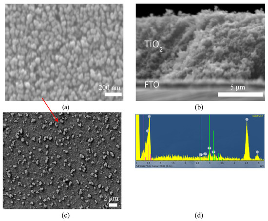
Figure 1.
Scanning electron microscope (SEM) images for a bare TiO2 film on fluorine-doped indium tin oxide (FTO) substrate (a) top view and (b) cross section, (c) SEM image of Ag-TiO2 film and (d) energy-dispersive spectrometry (EDS) of Ag-TiO2 on FTO substrate.
TEM was employed on Ag-TiO2 films in order to further investigate the surface morphology and the size of the AgNPs. TiO2 nanoparticles (Figure 2a,b) exhibit the shape of platelets with external large dimension of 20–45 nm, in agreement with the specifications of the Dyesol and/or P25 products. AgNPs (Figure 2c,d) form different structures; in some cases plate-like, when they are deposited on TiO2 films with average diameter of 15 nm. High-resolution TEM (HR-TEM) imaging, Figure 2c, permitted easy differentiation of Ag nanocrystals (small dark areas) and TiO2 crystallites (large bright areas). Ag nanocrystals can be observed on the surface of the TiO2 particles as dark lines. It is presumed that even smaller Ag nanoparticles are in existence scattered throughout the porous TiO2 surface.
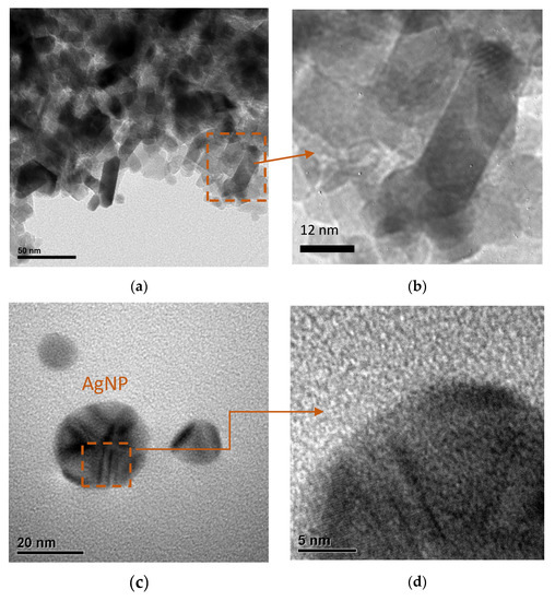
Figure 2.
Transmission electron microscope (TEM) images (a,b) of TiO2 at low TEM resolution and high-resolution TEM (HR-TEM) images (c,d) of Ag-TiO2 composites. Images, a and c, on the left have been magnified at the selected dotted squares and placed to the right as b and d, respectively.
The color change of the Ag-TiO2 films is significant upon bias application. Figure 3 presents the thin films of TiO2 as prepared from Dyesol (Figure 3a) and from Degussa (Figure 3d). After immersing the TiO2 films in the AgNPs solution the film color changes (Figure 3b), since AgNPs were adsorbed on the TiO2 film. In order to perform the electrochemical measurements, negative bias was applied in the film and the color of the film became darker (Figure 3c,e).
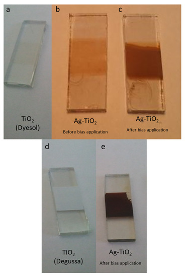
Figure 3.
Digital photos (a) mesoporous TiO2 film as fabricated from Dyesol and (d) from Degussa precursors. Ag-TiO2 films (b) before and (c,e) after bias application.
In order to investigate any changes in the crystal structure of the TiO2 films affected by the AgNPs, the XRD patterns (Figure 4) of FTO-conducting substrates, TiO2 and Ag-TiO2 film electrodes were measured. The XRD of TiO2 and AgNPs-TiO2 electrodes revealed similar characteristic peaks at 2θ: 25.28°, 37.8° and 48.05° which correspond to the indices of anatase TiO2 (101), (004) and (200) hkl planes and are consistent with the reported values of the JCPDS file (21-1272). As expected, no characteristic peaks that correspond to the rutile TiO2 indices were observed since the Dyesol TiO2 paste is 100% anatase. The only difference was observed on the relative intensities of the peaks, which may be due to the fact that doping alters the crystallinity but not the crystal structure of the Ag-TiO2 films. In addition, two slightly intense peaks at 26.54° and 38° which correspond to the plane indices 110 and 200 of the FTO glass could be observed. The XRD pattern of the AgNPs-TiO2 film showed a new peak at 44.4° which can be assigned to the (200) plane of Ag. Furthermore, a closer look of the peak at 38° of the Ag-TiO2, which corresponds to the (200) FTO index, also showed a small shoulder at 38.1° which can be assigned to the Ag (111) plane. These two peaks agree with the JCPDs card of Ag as presented in Figure 4. No rutile phase or any other modification is observed for the Ag-TiO2 film depending on AgNPs incorporation.
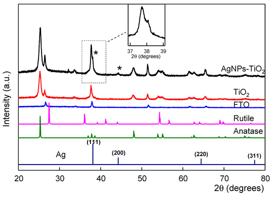
Figure 4.
X-ray diffraction (XRD) patterns of a TiO2 film with or without silver nanoparticles (AgNPs) deposited on its surface, FTO glass and Joint Committee on Powder Diffraction Standards (JCPDS) cards of anatase and rutile TiO2. Inset: magnification of the peak at 38ο corresponding to the fcc Ag (111) plane.
The TiO2 films deposited on conducting FTO glass slides had been soaked in solutions of AgNPs and rinsed with NaH2PO4 buffer to remove any loosely bound nanoparticles. The mp TiO2 films combine transparency in the visible region of the electromagnetic spectrum with a high surface area accessible to molecules from a surrounding solution (e.g., AgNPs). In many cases in the past, this allowed the adsorbed molecules (dyes, proteins, electrochromic species and surfactants) to achieve the densities required for informative electronic absorption spectroscopy, whether that was for the development of solar cells, electrochemical biosensors, electrochromic devices or catalytic applications [3,4,9,27,38,39]. Therefore, the transparency of the electrodes can be useful as it could allow the AgNPs adsorption process and their electrochromic properties to be monitored by UV–Vis absorption spectroscopy, which is a technique also used by other authors for the structural characterization of the AgNPs in a dielectric matrix [27,38,39,40,41].
Figure 5 shows the optical absorption spectra of the AgNPs solution used as dopants for the surface of the TiO2 films. A relatively broad absorption band is located at 452 nm properly corresponding to the size and form of the AgNPs; this peak is due to the SPR of the AgNPs and is within the spectrum range (400–450 nm) reported for them depending on their shape and size [27,30,38,39,41]. Adsorption of AgNPs on TiO2 films results in light coloration (see Figure 3) of the films, indicating that a large amount of AgNPs has been immobilized into the mesoporous TiO2 film. Also shown is the absorption spectrum of a bare TiO2 film which is transparent and colourless in the visible region, showing a characteristic absorption increase below 400 nm due to the onset of TiO2 band gap excitation. Therefore, the optical transparency of the TiO2 allows the adsorption process of the AgNPs to be monitored by UV–Vis absorption [30,42]. The electronic absorption spectra (Figure 5) for the nanocomposite Ag-TiO2 film showed features typical of AgNPs superimposed on a background arising from scattering by the TiO2 layer. The resulting spectrum of AgNPs on the TiO2 film showed a characteristic absorption band at 413 nm (a clear blue shift in comparison with the absorption spectra of the AgNPs in solution). The Ag-TiO2 film exhibits a much narrower, blue shift and more defined optical spectrum which means that the active metallic cores of the deposited AgNPs are smaller than those in the solution and probably spherical [27,38,41,43]. The shift is related to the size of the AgNPs and to the interaction between TiO2 and Ag, as well as to the fact that the majority of the AgNPs that have filled the pores are smaller than the pores themselves. No band is observed of organic residuals, which were used to bind the TiO2 nanoparticles, remaining in the film due to the titania film sintering at 450 °C. If the observed plasmonic bands were broad between 510 and 590 nm, that would have implied that the nanoparticles are large and/or of non spherical nature [44]. Increasing the AgNO3 solution concentration, where the AgNPs were created, had as a result the increase of the absorbance of the Ag-TiO2 film, as was also reported by other researchers in the past [30]. There is also the possibility that some of the non-reduced silver ions (Ag+) could be adsorbed on the hydroxylated TiO2 surface according to the following reaction, as suggested by other authors also in the past: Ag+ + TiO2− → Ti–O–Ag + H+ [45].
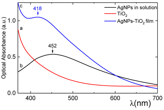
Figure 5.
Optical absorption spectra in the visible range (380–700 nm) of (a) AgNPs solution, (b) TiO2 film and (c) Ag-TiO2 film.
The plasmon resonance in the Ag-TiO2 thin films strongly depends on the crystalline phase and dielectric constant of the TiO2 matrix [46]. In theory, the SPR peak wavelength increases with increasing dielectric constant of the matrix and depends on the refractive index.
It should be mentioned that the form of the absorption profile does not only signify that the 415 nm absorption peak of the Ag-TiO2 films is characteristic of spherical AgNPs. It also carries information due to the band absence between 520 and 540 nm which is usually related to bigger AgNPs or AgNPs dimmers. Similarly, no band is observed around 620 nm which is usually due to non-spherical Ag nanoparticles or to larger particles or to manifestation of higher-order plasmon modes called quadrupolar modes. No band is also observed around 670 nm which suggests a longitudinal plasmon band of Ag nanorods. Any broadness of the observed absorption bands could refer to different morphologies of the deposited nanoparticles, to broad particle size distribution, and to agglomeration processes, while all the above discussion is in agreement with the TEM analysis.
The optical band gap of the Ag-TiO2 films is expected to be smaller to that of pure (blank) TiO2 films due to the effect of the AgNPs, as decrease of Eg with silver addition has also been reported by other authors [27,38,39,41]. Also, the Ag+ ions probably exist on the surface of the anatase TiO2 films by forming Ag–O–Ti bonds [47], which may introduce trap states affecting the energy band gap. Finally, it is possible that the potential applied can oxidize or reduce the Ag nanoparticles to silver oxide and reverse this as suggested by Kuzma et al [48].
Figure 6 presents the spectroelectrochemical spectrum for a Ag-TiO2 film electrode after remaining for 2 min at each negative applied potential (−0.1 to −1.1 V) applied. The plasmon (or Soret) band at 413 nm up until the application of −0.4 V remains constant, but upon the application of −0.5 V, it starts to increase in intensity without though changing shape. The application of −0.6 V to the film causes a big increase of the peak which at the same time becomes thinner and sharper. Afterwards, and by gradually applying more negative biases up to −1.1 V, the peak at 413 nm continues to rise and at the same time becomes sharper. However, several minutes after the end of the spectroelectrochemical measurements and the application of no voltage, the absorbance of the film shows that it has not returned to its initial state, but rather a shift of the main peak from 413 nm to 440 nm has been observed.
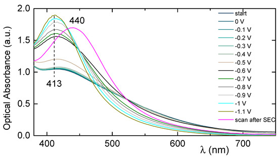
Figure 6.
Ultraviolet–visible (UV–Vis) spectral changes of a Ag-TiO2 film electrode upon the application of increasingly negative potentials (0 to −1.1 V vs. Ag/AgCl).
Following this route, increasing negative biases (−0.2 to −0.9) were applied again to the doped film and its absorption spectra were recorded. Figure 7 shows that upon the application of up to −0.4 V, a small increase in the size of the peak at 440 nm was monitored and a slight blue shift. However, upon the application of higher negative biases (−0.8 or −0.9 V) the peak shifts back to 413 nm. Figure 7 also shows that upon the application of a positive bias (0 to 0.6 V) the peak shifts again to 440 nm. The switch from 413 nm to 440 nm, depending on the bias that was applied to the film, was repeated several times and always with success.
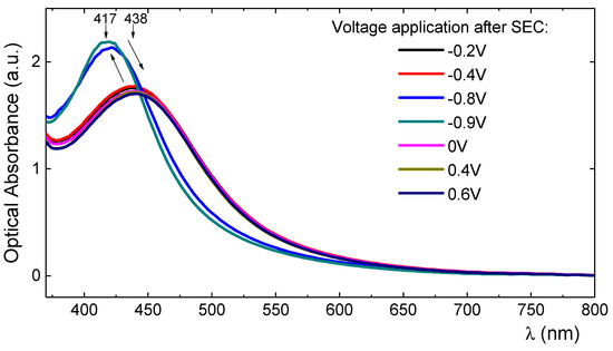
Figure 7.
UV–Vis spectral changes of a Ag-TiO2 film electrode under the application of negative or positive potentials showing the shift of the Soret peak from 413 nm to 440 nm and vice versa.
In order to gain an insight into the kinetic mechanism, the optical absorbance (OA) or optical density (OD) were measured for a range of negative and positive voltages. Figure 8a,b show the curves regarding the kinetics for the absorption change at 413 (a) and 440 nm (b) respectively. The absorbance was initially monitored during the application of −0.8 V for 600 s and immediately afterwards upon the application of 0.15 V for another 600 s. Figure 8a demonstrates that the continuous application of a sufficient cathodic current (−0.8 V) causes the fast increase of the absorbance at 413 nm of the Ag-TiO2 film in 4.5 s (τ1/2 = 2.6 s). By stepping back the potential from −0.8 V to +0.15 V, the absorbance at 413 nm starts dropping quite fast at the first 20 s and slower afterwards until it reaches the OD value it exhibited before the application of the negative bias. Similar results were obtained in Figure 8b for the kinetics for the absorption change at 440 nm. The continuous application of the −0.8 V caused the fast increase of OD at 440 nm of the Ag-TiO2 in 6 sec (τ1/2 = 3.8 s). The application of the +0.15 V caused the gradual drop of the OD at 440 nm and reached completion after 50 s.
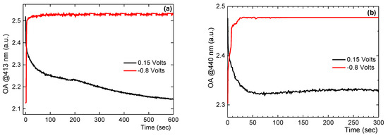
Figure 8.
Kinetics for the absorption change at 413 nm (a) and 440 nm (b) of a 6 μm thick Ag-TiO2 film by the application of 0.15 V and −0.8 V.
The spectroelectrochemical studies reported in Figure 6 and Figure 7 were further supported by cyclic voltammetry (CV). The CVs of mp TiO2 films with or without the adsorption of AgNPs on their surface, in aqueous 10 mM NaH2PO4 electrolyte of pH 7, at a scan rate of 0.1 V/s, are presented in Figure 9. Upon scanning the potential of a bare semiconductive TiO2 film cathodically in a neutral pH aqueous medium (NaH2PO4, pH 7), a transition from insulating to conductive behaviour is observed. The characteristic charging/discharging currents were assigned to electron injection and storage into sub-band gap/conduction band states of the TiO2 film, until the metal oxide becomes fully degenerated once the applied potential reaches the conduction band potential [9,33,34,49]. The current shows a plateau at potentials where the film behaves as an insulator (positive biases and up to around −0.3 V). At that range the electrical response is dominated by the Helmholtz capacity of the uncovered FTO glass/electrolyte solution interface at the bottom of the TiO2 film [50,51]. At more negative potentials (−0.3 V and higher), the cathodic current displays an exponentially rising behaviour (at −0.8 V) that is considered by many authors as the reduction of superficial Ti ions [52,53]. This rising behaviour is then transformed to a peak (at −0.75 V), when the direction of voltammetry is reversed to anodic. This is considered as re-oxidation of reduced Ti ions and is a slow and irreversible process [53]. These potentials are more negative than the conduction band potential and the TiO2 film behaves as a conductive metallic electrode. As the scan rate becomes slower (Figure 10) the height of the anodic peak progressively diminishes until, at very slow scan rates (0.01 V/s), it disappears. According to many reports [1,7,53,54] the origin of this behaviour is due to the charging/discharging of electrons in the film and a charge transfer mechanism. However, no cathodic or anodic peaks due to a redox reaction are observed. The CV integrates to approximately 0, indicating negligible Faradaic currents.
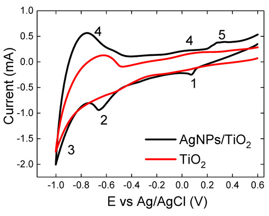
Figure 9.
Cyclic voltammograms (CVs) in 10 mM NaH2PO4 buffer, pH 7 for Ag-TiO2 and blank TiO2 films. The scan rate was 0.1 V/s.
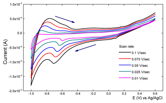
Figure 10.
Cyclic voltammograms (CVs) in 10 mM NaH2PO4 buffer pH 7, for a Ag-TiO2 film at different scan rates.
In addition, Figure 9 shows the CV of a TiO2 film electrode after the adsorption of AgNPs on its surface. The Ag-TiO2 film exhibited two pairs of redox peaks that were absent from the CV of the bare TiO2 film. For the first pair, a small cathodic peak is observed at +0.07 V and a small anodic peak at +0.27 V. For the second pair the cathodic peak is much bigger and appears at −0.65 V and the anodic peak which is much smaller and broader appears around −0.53 V. All these peaks are attributed to two different reduction/oxidation states of Ag on the TiO2 films. The redox reactions are associated with Ag → Ag2O and Ag2O → Ag (oxidation and reduction peaks, respectively) [55,56]. The pair of peaks at the lower biases correspond to the reduction and oxidation of the AgNPs that have adsorbed inside the mesoporous network of the TiO2 film and the other pair of smaller peaks most probably correspond either to small deposited AgNPs or to AgNPs adsorbed only on the outer surface of the TiO2 film [46]. Also both re-oxidation peaks are broader and smaller to the reduction peaks due to the large band gap of the TiO2 film. This observation most probably requires further experiments in order to draw any final conclusions. However, this redox behaviour (two sets of redox peaks, a two phase reduction) of the AgNPs on the TiO2 films has also been monitored on immobilization studies of a heme based redox dyes, such as iron(III) 5,10,15,20-tetrakis(1-methyl-4-pyridyl) porphyrin, FeTMPyP, on the same films [33].
The effect of the scan rate on the voltammetric behaviour of the Ag-TiO2 film was also investigated. Slower scan rates were applied to the Ag-TiO2 electrode in order to try to obtain a reversible peak-shaped CV. Figure 10 illustrates that even at slow scan rates no simple reversible behaviour for the Ag-TiO2 film was observed, consistent with the currents being limited by the low TiO2 conductivity at moderate potentials. However, the cathodic peak potential at −0.65 V shifted negatively with the increase of the scan rate. In addition, there is a good linear relationship between the cathodic peak current and the scan rate in the range (0.01 to 0.1 V/s), indicative of a surface-confined electrochemical process. This has also been observed in other systems where instead of AgNPs, surfactants or proteins were adsorbed on the TiO2 films [39].
Also, it was found that the cathodic and anodic peak currents corresponding to the adsorbed AgNPs vary linearly with scan rates in the range of 10 to 100 mV·s–1. The CVs exhibit a current increase as the scan rates are steadily increased, significantly larger when the 0.1 V/s scan rate results are compared to those of the 0.01 V/s. This is clear indication that the adsorbed AgNPs underwent a surface-controlled process.
4. Conclusions
All the above experimental data clearly suggest that the electrophotochromism of the Ag-TiO2 composite is due to oxidation/reduction of the Ag nanoparticles, which forms a thin layer of Ag2O on the metallic core, forming core/shell nanoparticles; the core is metallic while the outer shell is semiconducting, where the peaks agree well with those found by Kuzma et al. [46]. In fact, it is suggested that the oxide thickness is about 1.5 nm when the composite absorbs at the 440 nm peak and at most 0.5 nm while the composite exhibits a peak at 413 nm. Furthermore, it is possible that the particles may be charged upon the application of negative potential on the Ag-TiO2 electrode, which would lead their separation due to their charging; such an effect would not be possible at positive electrode potentials since silver has a lower conduction band than that of the FTO electrode and than that of TiO2.
Supplementary Materials
The following are available online at https://www.mdpi.com/2079-6412/10/2/130/s1.
Author Contributions
E.T. and I.K. conceived and designed the experiments; S.K., J.P., E.T. and I.K. performed the experiments; E.T., I.K., S.K. and J.P. analyzed the data; E.T. and I.K. contributed reagents/materials/analysis tools; I.K., S.K., E.T. and J.P. wrote the paper. All authors have read and agreed to the published version of the manuscript.
Funding
This research received no external funding from funding agencies in the public, commercial or not-for-profit sectors.
Acknowledgments
We would like to thank Nikolaos Boukos from NCSR “Demokritos” for the TEM images.
Conflicts of Interest
The authors declare no conflict of interest.
References
- Garoz-Ruiz, J.; Ibañez, D.; Romero, E.C.; Ruiz, V.; Heras, A.; Colina, A. Optically transparent electrodes for spectroelectrochemistry fabricated with graphene nanoplatelets and single-walled carbon nanotubes. RSC Adv. 2016, 6, 31431–31439. [Google Scholar] [CrossRef]
- Ellmer, K. Past achievements and future challenges in the development of optically transparent electrodes. Nat. Photonics 2012, 6, 809–817. [Google Scholar] [CrossRef]
- Topoglidis, E.; Lutz, T.; Durrant, J.R.; Palomares, E. Interfacial electron transfer on cytochrome-c sensitized conformally coated mesoporous TiO2 films. Bioelectrochemistry 2008, 74, 142–148. [Google Scholar] [CrossRef] [PubMed]
- O’Regan, B.; Gratzel, M. A low cost high-efficiency solar-cell on dye-sensitized colloidal TiO2 films. Nature 1991, 353, 3737–3740. [Google Scholar] [CrossRef]
- Xin, B.F.; Ren, Z.Y.; Hu, H.Y.; Zhang, X.Y.; Dong, C.L.; Shi, K.Y.; Jing, L.Q.; Fu, H.G. Photocatalytic activity and interfacial carrier transfer of Ag-TiO2 nanoparticle films. Appl. Surf. Sci. 2005, 252, 2050–2055. [Google Scholar] [CrossRef]
- Sarkar, J.; John, V.T.; He, J.; Brooks, C.; Gandhi, D.; Nunes, A.; Ramanath, G.; Bose, A. Surfactant-templated, synthesis and catalytic properties of patterned nanoporous titania supports loaded with platinum nanoparticles. Chem. Mater. 2008, 20, 5301–5306. [Google Scholar] [CrossRef]
- Rodriguez, J.A.; Evans, J.; Graciani, J.; Park, J.B.; Liu, P.; Hrbek, J.; Sanz, J.F. High water-gas shift activity in TiO2(110) supported Cu and Au nanoparticles: Role of the oxide and metal particle size. J. Phys. Chem. C 2009, 113, 7364–7370. [Google Scholar] [CrossRef]
- Zhao, G.L.; Kozuka, H.; Yoko, T. Sol-gel preparation and photoelectrochemical properties of TiO2 films containing Au and Ag metal particles. Thin Solid Film. 1996, 277, 147–154. [Google Scholar] [CrossRef]
- Topoglidis, E.; Campbell, C.J.; Cass, A.E.G.; Durrant, J.R. Factors that affect protein adsorption on nanostructured titania films, A novel spectroelectrochemical application to sensing. Langmuir 2001, 17, 7899–7906. [Google Scholar] [CrossRef]
- Ha, T.-J.; Hong, M.-H.; Park, C.-S.; Park, H.-H. Gas sensing properties of ordered mesoporous TiO2 film enhanced by thermal shock induced cracking. Sens. Actuat. B Chem. 2013, 181, 874–879. [Google Scholar] [CrossRef]
- Feng, J.; Han, J.; Zhao, X. Synthesis of CuInS2 quantum dots on TiO2 porous films by solvothermal method for absorption layer of solar cells. Prog. Org. Coat. 2009, 64, 268–273. [Google Scholar] [CrossRef]
- Gao, X.F.; Li, H.B.; Sun, W.T.; Chen, Q.; Tang, F.Q.; Peng, L.M. CdTe quantum dots-Sensitized TiO2 nanotube array photoelectrodes. J. Phys. Chem. C 2009, 113, 7531–7535. [Google Scholar] [CrossRef]
- Giordano, F.; Abate, A.; Correa Baena, J.P.; Saliba, M.; Matsui, T.; Im, S.H.; Zakeeruddin, S.M.; Nazeeruddin, M.K.; Hagfeldt, A.; Graetzel, M. Enhanced electronic properties in mesoporous TiO2 via lithium doping for high-efficiency perovskite solar cells. Nat. Commun. 2016, 7, 10379. [Google Scholar] [CrossRef] [PubMed]
- Cinnsealach, R.; Boschloo, G.; Rao, S.N.; Fitzmaurice, D. Coloured electrochromic windows based on nanostructured TiO2 films modified by adsorbed redox chromophores. Sol. Energy Mater. Sol. Cells 1999, 57, 107–125. [Google Scholar] [CrossRef]
- Zhang, X.; Fujishima, A.; Jin, M.; Emeline, A.V.; Murakami, T. Double-layered TiO2-SiO2 nanostructured films with self-cleaning and antireflective properties. J. Phys. Chem. B 2006, 110, 25142–25148. [Google Scholar] [CrossRef]
- Singhal, A.; Skandan, G.; Amatucci, G.; Badway, F.; Ye, N.; Manthiram, A.; Ye, H.; Xu, J.J. Nanostructured electrodes for next generation rechargeable electrochemical devices. J. Power Sources 2004, 129, 38–44. [Google Scholar] [CrossRef]
- Hecht, D.S.; Hu, L.; Irwin, G. Emerging transparent electrodes based on thin films of carbon nanotubes, graphene, and metallic nanostructures. Adv. Mater. 2011, 23, 1482–1513. [Google Scholar] [CrossRef]
- Cao, W.; Li, J.; Chen, H.; Xue, J. Transparent electrodes for organic optoelectronic devices: A review. J. Photonics Energy 2014, 4, 40990. [Google Scholar] [CrossRef]
- Weng, Z.; Guo, H.; Liu, X.; Wu, S.; Yeung, K.; Chu, P.K. Nanostructured TiO2 for energy conversion and storage. RSC Adv. 2013, 3, 24758–24775. [Google Scholar] [CrossRef]
- Chen, C.; Conception, J.J.; Jurss, J.W.; Meyer, T.J. Single-Site, Catalytic Water Oxidation on Oxide Surfaces. J. Am. Chem. Soc. 2009, 131, 15580–15581. [Google Scholar] [CrossRef]
- Xie, K.; Sun, L.; Wang, C.; Lai, Y.; Wang, M.; Chen, H.; Lin, C. Photocatalytic properties of Ag nanoparticles loaded TiO2 nanotube arrays prepared by pulse current deposition. Electrochim. Acta 2010, 55, 7211–7218. [Google Scholar] [CrossRef]
- Swarnakar, P.; Kanel, S.R.; Nepal, D.; Jiang, Y.; Jia, H.; Kerr, L.; Goltz, M.N.; Levy, J.; Rakovan, J. Silver deposited titanium dioxide thin film for photocatalysis of organic compounds using natural light. Solar Energy 2013, 88, 242–249. [Google Scholar] [CrossRef]
- Cheng, B.; Le, Y.; Yu, J. Preparation and enhanced photocatalytic activity of Ag@TiO2 core–shell nanocomposite nanowires. J. Hazard. Mat. 2010, 177, 971–977. [Google Scholar] [CrossRef] [PubMed]
- Palomares, E.; Vilar, R.; Durrant, J.R. Heterogeneous colorimetric sensor for mercuric salts. Chem. Commun. 2004, 362–363. [Google Scholar] [CrossRef]
- Mandal, S.S.; Bhattacharyya, A.J. Electrochemical sensing and photocatalysis using Ag-TiO2 microwires. J. Chem. Sci. 2012, 124, 969–978. [Google Scholar] [CrossRef]
- Jiang, Y.; Zheng, B.; Du, J.; Liu, G.; Guo, Y.; Xiao, D. Electrophoresis deposition of Ag nanoparticles on TiO2 nanotube arrays electrode for hydrogen peroxide sensing. Talanta 2013, 112, 129–135. [Google Scholar] [CrossRef] [PubMed]
- Ivanova, T.; Harizanova, A.; Koutzarova, T.; Vertuyen, B. Optical and structural characterization of TiO2 films doped with silver nanoparticles obtained by a sol-gel method. Opt. Mater. 2013, 36, 207–213. [Google Scholar] [CrossRef]
- Djaoued, Y.; Ozga, K.; Wojciechowski, A.; Reshak, A.H.; Robichaud, J.; Kityk, I.V. Photoinduced effects in TiO2 nanocrystalline films with different morphology. J. Alloys Compd. 2010, 508, 599–605. [Google Scholar] [CrossRef]
- Anandan, S.; Sathish Kumar, P.; Pugazhenthiran, N.; Madhavan, J.; Maruthamuthu, P. Effect of loaded silver nanoparticles for photocatalytic degradation of Acid Red 88. Sol. Energy Mater. Sol. Cells 2008, 92, 929–937. [Google Scholar] [CrossRef]
- Stathatos, E.; Lianos, P.; Falaras, P.; Siokou, A. Photocatalytically deposited silver nanoparticles on mesoporous TiO2 films. Langmuir 2000, 16, 2398–2400. [Google Scholar] [CrossRef]
- Tricot, F.; Vocanson, F.; Chaussy, D.; Beneventi, D.; Reynaud, S.; Lefkir, Y.; Destouches, N. Photochromic Ag:TiO2 thin films on PET substrate. RSC Adv. 2014, 4, 61305–61312. [Google Scholar] [CrossRef]
- Okumu, J.; Dahmen, C.; Sprafke, A.N.; Luysberg, M.; von Plessen, G.; Wuttig, M. Photochromic silver nanoparticles fabricated by sputter deposition. J. Appl. Phys. 2005, 97, 094305. [Google Scholar] [CrossRef]
- Ohko, Y.; Tatsuma, T.; Fujii, T.; Naoi, K.; Niwa, C.; Kubota, Y.; Fujishima, A. Multicolour photochromism of TiO 2 films loaded with silver nanoparticles. Nat. Mater. 2003, 2, 29–31. [Google Scholar] [CrossRef]
- Hou, W.; Cronin, S.B. A review of surface plasmon resonance-enhanced photocatalysis. Adv. Funct. Mater. 2013, 23, 1612–1619. [Google Scholar] [CrossRef]
- Wu, C.; Mosher, B.P.; Lyons, K.; Zeng, T. Reducing Ability and Mechanism for Polyvinylpyrrolidone (PVP) in Silver Nanoparticles Synthesis. J. Nanosci. Nanotechnol. 2010, 10, 2342–2347. [Google Scholar] [CrossRef]
- Zhang, S.; Tang, Y.; Vlahovic, B. Preparation of Silver Nanoparticles in Poly(N-vinylpyrrolidone)/Ethanol Solutions. Int. J. Nanosci. Ser. 2017, 16, 1750008. [Google Scholar] [CrossRef]
- Mierzwa, M.; Lamouroux, E.; Walcarius, A.; Etiene, M. Porous and transparent metal-oxide electrodes: Preparation methods and electroanalytical application prospects. Electroanalysis 2018, 30, 1241–1258. [Google Scholar] [CrossRef]
- Hirakawa, T.; Kamat, P.V. Charge separation and catalytic activity of Ag@TiO2 core-shell composite clusters under UV-irradiation. J. Am. Chem. Soc. 2005, 127, 3928–3934. [Google Scholar] [CrossRef]
- Nadar, L.; Sayah, R.; Vocanson, F.; Crespo-Montteiro, N.; Boukenter, A.; Joao, S.S.; Destouches, N. Influence of reduction process of the colour and photochromism of amorphous mesoporous TiO2 thin films loaded with a silver salt. Photochem. Photobiol. Sci. 2011, 10, 1810–1816. [Google Scholar] [CrossRef]
- Kawahara, K.; Suzuki, K.; Okho, Y.; Tatsuma, T. Electron transport in silver-semiconductor nanocomposite films exhibiting multicolor photochromism. Phys. Chem. Chem. Phys. 2005, 7, 3851–3855. [Google Scholar] [CrossRef]
- Awazu, K.; Fujimaki, M.; Rockstuhl, C.; Tominaga, J.; Murakami, H.; Ohki, Y.; Yoshida, N.; Wanatabe, T. A plasmonic photocatalyst consisting of silver nanoparticles embedded in titanium dioxide. J. Am. Chem. Soc. 2008, 130, 1676–1680. [Google Scholar] [CrossRef] [PubMed]
- He, J.; Ichinose, I.; Kunitake, T.; Nakao, A. In situ synthesis of noble metal nanoparticles in ultrathin TiO2-Gel films by a combination of on ion-exchange and reduction processes. Langmuir 2002, 18, 10005–10010. [Google Scholar] [CrossRef]
- Gharibshahi, L.; Saion, E.; Gharibshahi, E.; Shaari, A.H.; Matori, K.A. Structural and Optical Properties of Ag Nanoparticles Synthesized by Thermal Treatment Method. Materials 2017, 10, 402. [Google Scholar] [CrossRef]
- Sun, Y.; Xia, Y. Triangular Nanoplates of Silver: Synthesis, Characterization, and Use as Sacrificial Templates for Generating Triangular Nanorings of Gold. Adv. Mater. 2003, 15, 695–698. [Google Scholar] [CrossRef]
- Arabatzis, I.M.; Stergiopoulos, T.; Bernard, M.C.; Labou, D.; Neophytides, S.G.; Falaras, P. Silver-modified titanium dioxide thin films for efficient photodegradation of methyl orange. Appl. Catal. B Environ. 2003, 42, 187–201. [Google Scholar] [CrossRef]
- Couzon, N.; Maillard, M.; Bois, L.; Chassagneux, F.; Brioude, A. Electrochemical observation of the plasmonic effect in photochromic Ag nanoparticle filled mesoporous TiO2 film. J. Phys. Chem. C 2017, 121, 22147–22155. [Google Scholar] [CrossRef]
- Yu, B.; Leung, K.M.; Guo, Q.; Lau, W.M.; Yang, J. Synthesis of Ag-TiO2 composite nano thin film for antimicrobial application. Nanotechnology 2011, 22, 115603. [Google Scholar] [CrossRef]
- Kuzma, A.; Weis, M.; Flickyngerova, S.; Jakabovic, J.; Satka, A.; Dobrocka, E.; Chlpik, J.; Cirak, J.; Donoval, M.; Telek, P.; et al. Influence of surface oxidation on plasmon resonance in monolayer of gold and silver nanoparticles. J. Appl. Phys. 2012, 112, 103531. [Google Scholar] [CrossRef]
- Kim, Y.S.; Balland, V.; Limoges, B.; Costentin, C. Cyclic Voltammetry modelling of proton transport effects on redox charge storage in conductive materials: Application to a mesoporous TiO2 film. Phys. Chem. Chem. Phys. 2017, 19, 17944–17951. [Google Scholar] [CrossRef]
- Fabregat-Santiago, F.; Randriamahazaka, H.; Zaban, A.; Garcia-Canadas, J.; Garcia-Belmonte, G.; Bisquert, J. Chemical capacitance of nanoporous-nanocrystalline TiO2 in a room temperature ionic liquid. Phys. Chem. Chem. Phys. 2006, 8, 1827–1833. [Google Scholar] [CrossRef]
- Fabregat-Santiago, F.; Garcia-Belmonte, G.; Bisquert, J.; Bogdanoff, P.; Zaban, A. Mott-Schottky analysis of nanoporous semiconductor electrodes in dielectric state deposited on SnO2 (F) conducting substrates. J. Electrochem. Soc. 2002, 150, E293. [Google Scholar] [CrossRef]
- Lyon, L.A.; Hupp, J.T. Energetics on the nanocrystalline titanium dioxide/aqueous solution interface: Approximate conduction band edge variations between H0 = −10 and H− = +26. J. Phys. Chem. B 1999, 103, 4623–4628. [Google Scholar] [CrossRef]
- Cuteo-Gomez, L.F.; Garcia-Gomez, N.A.; Mosqueda, H.A.; Sanchez, E.M. Electrochemical study of TiO2 modified with silver nanoparticles upon CO2 reduction. J. Appl. Electrochem. 2014, 44, 675–682. [Google Scholar] [CrossRef]
- Renault, C.; Nicole, L.; Sanchez, C.; Costentin, C.; Balland, V.; Limoges, B. Unraveling the charge transfer/electron transport in mesoporous semiconductive TiO2 films by voltabsoptometry. Phys. Chem. Chem. Phys. 2015, 17, 10592–10607. [Google Scholar] [CrossRef]
- Wang, G.F.; Li, M.G.; Gao, Y.C.; Fang, B. Amperometric sensor used for determination of thiocyanate with a silver nanoparticles modified electrode. Sensors 2004, 4, 147–155. [Google Scholar] [CrossRef]
- Chang, G.; Zhang, J.; Oyama, M.; Hirao, K. Silver-nanoparticle-attached indium tin oxide surfaces fabricated by a seed-mediated growth approach. J. Phys. Chem. B 2005, 109, 1204–1209. [Google Scholar] [CrossRef]
© 2020 by the authors. Licensee MDPI, Basel, Switzerland. This article is an open access article distributed under the terms and conditions of the Creative Commons Attribution (CC BY) license (http://creativecommons.org/licenses/by/4.0/).