Abstract
In this paper, integration of silicon oxycarbide (SiOC) and silicon nitride (Si3N4) platforms was demonstrated to realize ultra-efficient thermal tuning of photonic integrated circuits. Si3N4 being a fascinating photonic material with moderate refractive index (n ≈ 2) and ultra-low loss, lacks thermo-optic coefficient that makes thermal phase actuators long and dissipate high powers. Integration of SiOC coating with a comparable refractive index (n = 2.2) boosts the effective thermo-optic efficiency of Si3N4 photonic circuits by almost an order of magnitude with no additional loss. An SiOC layer was deposited by the reactive RF magnetron sputtering technique from the SiC target at room temperature. The structural, chemical and optical characterizations of the sputter deposited SiOC layer were performed with SEM, AFM, EDS and spectroscopic ellipsometry. The results of SiOC-coated Si3N4 and pristine Si3N4 photonic devices were discussed and compared. SiOC was demonstrated as an enabling platform for low-loss and power-efficient thermal phase actuators in conventional photonic technologies with application in reconfigurable photonic systems.
1. Introduction
Silicon photonic integration has advanced significantly in the past decades and is perceived to take advantage of the complementary metal oxide semiconductor (CMOS) industry [,]. Silicon (Si) photonic devices, being very high contrast with silica cladding, confine light tightly into the core and are prone to fabrication tolerances and side-wall roughness, contributing to losses [,]. Hence research into Si-based material platforms has received attention in recent years. Silicon nitride (Si3N4) is an attractive material for its moderately high refractive index (n ≈ 2 at λ = 1550 nm) and low absorption coefficient (< 1 dB/m) in the visible and near-IR spectral regions [,]. Si3N4 photonic integrated circuits (PICs) have found applications in the fields of telecom, datacom, sensing, bio-photonics and optical signal processing [,]. Si3N4 has been deposited using CMOS compatible techniques, for example, low pressure chemical vapor deposition (LPCVD) and plasma enhanced chemical vapor deposition (PECVD). With its complementary features of wider wavelength transparency range and lower scattering losses, simple to complex PICs have been demonstrated. Further, Si3N4 is one of the platforms for which multi-project wafer (MPW) runs are offered. However, thermo-optic effect in Si3N4 is low, in the order of 10−5 °C−1, and requires long and wide thermal tuners with large power dissipation []. The large footprint of thermal tuners is contrary to the spirit of PICs that determines the ultimate cost of a photonic product. There are other ways of PIC reconfiguration such as electro-absorption and electro-refraction; however, the thermo-optic effect over the refractive index is larger, induces less losses, and therefore thermal tuners/heaters are simple and ubiquitous []. Recently, a novel photonic platform silicon oxycarbide (SiOC) with a wider refractive index tunable range from 1.45 to 3.0 and lower propagation losses of about 2 dB/cm in the near-infrared wavelength region has been demonstrated [,]. Furthermore, SiOC with a moderately high refractive index (n = 2.2 at λ = 1550 nm) has been shown to exhibit a highest thermo-optic coefficient of KSiOC = 2.5 × 10⁻⁴ °C−1, reported among the well-known dielectric technologies, that is thirty times larger than silica and almost twice that of silicon []. Ultra Si-rich nitride (SRN) with n = 3.0 is another material platform recently demonstrated to exhibit a high thermo-optic coefficient of KSiOC = 2.66 × 10⁻⁴ °C−1. However, the refractive index and the propagation losses (7.5 dB/cm) of the SRN platform are too high and thus confine its use [,]. Though several polymers and TiO2 have been shown to exhibit high negative values of thermo-optic coefficient that depend on the thermal expansion of the material, it fails when the material is covered by an upper cladding layer []. SiOC on the other hand is an appealing platform with a wide refractive index range that is significantly higher than that provided by other low-loss photonic platforms including silicon oxynitride (SiON) [], Si3N4 and Ta2O5 [] and no absorption peak in the 1550 nm wavelength band. The wider refractive index tunable range, low material losses and absence of absorption peak in the telecom window makes SiOC a promising photonic platform for telecom and sensing applications.
In this work, we aim to integrate SiOC with Si3N4 to enhance thermo-optic efficiency and demonstrate ultra-efficient thermal tuning of photonic circuit. Taking the advantages of high thermo-optic coefficient of SiOC and well-matured low-loss Si3N4, we propose integration of SiOC and Si3N4 platforms to realize power-efficient, thermally tunable photonic integrated circuits.
2. SiOC Layer Deposition and Characterizations
The geometry of SiOC-coated Si3N4 waveguides is shown in the Figure 1a. A Si3N4 chip already patterned with channel waveguides and ring resonator, and a bare Si substrate sample were mounted on a circular holder in the reactive RF magnetron sputtering chamber. The deposition of silicon oxycarbide was performed at low base pressure of 9 × 10⁻⁶ mbar using silicon carbide (SiC) target in the presence of argon (Ar) and oxygen (O) as plasma and reactive gases, respectively. The flow of Ar (10 sccm) and O (0.75 sccm) was maintained with mass flow controllers. The width and height of the Si3N4 strip waveguides were 1.2 μm and 0.3 μm, respectively. Cross-sectional images of SiOC-coated Si3N4 waveguides were obtained with a scanning electron microscope (SEM, Model: LEO 1525, One Zeiss Drive, NY, USA). Considering the dielectric nature of SiOC and Si3N4 layers, a thin platinum layer of about 4 nm was sputtered on the chip to avoid an electron charging effect. The SEM cross-section images were obtained by operating the electron gun at a voltage of 10 kV and collecting the signals from the in-lens detector. Figure 1b shows the SEM cross sectional image of Si3N4 waveguide covered with SiOC. The SiOC layer had a thickness of 350 nm, and the estimated deposition rate was 30 nm/min as the deposition was run for 10 min. Good adhesion between SiOC and Si3N4 layers was observed, showing lower possibility of interfacial scattering. The SiOC/Si3N4 structures were covered by PECVD silica with n = 1.45. The SiOC/Si sample was used for film characterizations, such as ellipsometry (VASE, J.A. Woollam Inc., Lincoln, NE, USA), atomic force microscopy (AFM Model: 5600LS AFM system, Keysight, CA, USA) and energy dispersive spectroscopy (EDS) analysis.

Figure 1.
(a) Geometry scheme and (b) SEM micrograph of SiOC-coated SiN waveguide.
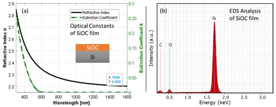
Figure 2a shows the refractive index n and extinction coefficient k spectra of SiOC film measured with spectroscopic ellipsometry over the wide wavelength range between 300 nm and 1600 nm. The measured ellipsometric quantities (psi ψ, del Δ) modeled by a Cody–Lorentz oscillator [] gave a good fit with simulated data and mean squared error (MSE) of less than two. The refractive index of the deposited SiOC film at standard telecom wavelength 1550 nm was measured as n = 2.2 with negligible extinction coefficient (k < 10−4) as the film exhibits high transparency above λ > 550 nm. The rms roughness of the sputtered SiOC layer surface was measured with atomic force microscope in tapping mode over an area of 100 μm2. The measured rms surface roughness was about 0.5 nm that was comparable to the substrate and further confirmed the smooth homogenous morphology of the deposited SiOC layer as observed by SEM images. The elemental analysis of sputtered SiOC film was performed with energy dispersive spectroscopy (EDS). EDS analysis of the SiOC film showed the presence of silicon (Si), carbon (C) and oxygen (O) elements with no impurities. The peaks of the Si, C and O elements are shown in the EDS spectrum given in Figure 2b. The elemental composition in SiOC film was quantified in atomic percent as Si (44 at. %), C (29 at. %) and O (27 at. %) with an error of ±2%.

Figure 2.
(a) Measured optical constants (n and k) spectra and (b) EDS analysis of SiOC thin film.
3. SiOC-Coated Si3N4 Device Simulation and Experimental Results
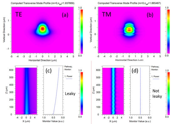
Electromagnetic simulations were performed in order to determine the effective index of fundamental modes, understand field propagation and calculate the confinement factor of the mode in the SiOC, Si3N4 and SiO2 layers of the waveguide. The fundamental transverse electric (TE) and transverse magnetic (TM) modes of SiOC-coated Si3N4 waveguides are shown in Figure 3a,b. The simulations revealed that the fundamental TE mode with neff = 1.937 at λ = 1550 nm was leaky over a π-length when a bend with radius 100 μm was considered, as shown in Figure 3c. The propagation of fundamental TM mode with neff = 1.865 was stable with negligible loss, as seen in Figure 3d. The confinement factor Γ is a useful parameter to determine the confinement of mode in each layer of the waveguide. Γ is used in estimating a material’s thermo-optic coefficient. Further details on the confinement factor Γ can be found in our previous publication []. The TM mode confinements in the different layers of silica buried SiOC-coated Si3N4 strip waveguides were Γ = 0.37 in SiOC, Γ = 0.28 in Si3N4, and Γ = 0.28 in SiO2. The simulations indicated that most of the TM mode light was confined in the SiOC layer that helped to boost the thermo-optic efficiency of the Si3N4 platform.

Figure 3.
Electromagnetic simulations of TE and TM fundamental modes and their propagation from silica buried SiOC-coated Si3N4 waveguide with a bend radius of 100 μm (a) TE mode (b) TM mode (c) propagation of TE mode that is leaky and (d) stable propagation of TM mode.
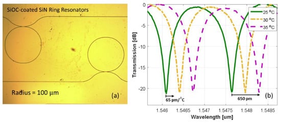
Figure 4a shows the optical micrograph of all-pass Si3N4 micro-ring resonators coated with SiOC and buried under PECVD silica. The radius of the ring resonator was 100 μm, the length of the coupler section was 12 μm and the circumference of the ring resonator was 640.3 μm. The Si3N4 micro-ring resonators were based on the rectangular waveguide geometry (1.2 × 0.3 μm2, see Figure 1) and refractive index 1.9963 at λ = 1550 nm. To perform optical measurements, the SiOC-coated Si3N4 chip was mounted on a stable stage of optical setup comprising of tunable laser, optical spectrum analyzer, polarization controller and thermoelectric Peltier module. Lensed optical fibers were used to launch the light from a tunable laser, and the polarization state of light was controlled with a polarization controller guaranteeing at least −30 dB crosstalk between TE and TM polarizations. TM polarized light was coupled to the SiOC-coated Si3N4 micro-ring resonator from a tunable laser operating in the broad spectral range from 1520 to 1580 nm.

Figure 4.
(a) Optical micrograph of SiOC-coated Si3N4 micro-ring resonators (b) optical transmission spectrum of ring resonator at different temperatures.
Figure 4b shows the measured transmission spectrum of a SiOC-coated Si3N4 micro-ring resonator around the wavelength λ = 1.55 μm at three different temperatures. The free spectral range (FSR) measured from the transmission spectra given in Figure 4b was estimated as 1.61 nm that resulted in the effective group index ng = 2.2834. The measured FSR and ng values closely matched the simulated values. The thermo-optic behavior was evaluated by optical transmission measurement of the fabricated SiOC-coated Si3N4 ring resonator at different temperatures. When the temperature was raised from room temperature 25 to 30 °C, a change in temperature dT = 5 °C, it led to the shift in the resonance of the ring resonator by 325 pm. Similarly, when the temperature was increased from 30 to 35 °C, and any additional temperature by dT = 5 °C, a same shift was measured that resulted in dλ/dT = 65 pm/°C. The effective thermo-optic coefficient referred to as Keff of the SiOC-coated Si3N4 ring resonator was estimated using the relation,
and substituting the measured values in the relation results in Keff = 9.5 × 10⁻⁵ °C−1 that is eight times larger than Si3N4 strip waveguides. Since the SiOC-coated Si3N4 ring resonator consists of three material layers of SiOC, Si3N4 and silica, the effective thermo-optic coefficient Keff can therefore be used to estimate the SiOC material thermo-optic coefficient. Since where is the thermo-optic coefficient and is the mode confinement factor in the ith material [], the can be written as,
Using Equation (2) and the measured value of Keff of the SiOC-coated Si3N4 ring resonator, the thermo-optic coefficient of SiOC was estimated as 2.4 × 10⁻⁵ °C−1, which is one order of magnitude larger than the Si3N4 material thermo-optic coefficient and the largest among dielectric platforms. The thermo-optic coefficients of silica ( = 0.9 × 10⁻⁵ °C−1) and ( = 2.5 × 10⁻⁵ °C−1) were considered in Equation (2).
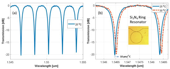
An identical Si3N4 ring resonator with the same waveguide dimensions (1.2 × 0.3 μm2) and n = 1.9963 at λ = 1550 nm was measured. The measured transmission spectrum of the silica cladding covered Si3N4 ring resonator at room temperature is shown in Figure 5a. The free spectral range estimated from the transmission spectrum was FSR = 1.9078 nm and the effective group index ng = 1.9666. The transmission spectrum measured at two temperatures (25 °C and 30 °C) is shown in Figure 5b. The increase in the temperature between 25 °C and 30 °C induced a shift of about 50 pm/°C and 10 pm/°C in the resonant wavelength. The effective thermo-optic coefficient of Si3N4 ring resonator as estimated from relation (1) is Keff = 1.26 × 10⁻⁵ °C−1 around λ = 1550 nm; similar results have been reported for Si3N4 waveguides [,]. Comparing the transmission spectra before and after SiOC deposition, no additional loss was observed.

Figure 5.
(a) Measured transmission spectrum of pristine Si3N4 ring resonator (b) transmission spectrum of pristine Si3N4 ring resonator at two different temperatures to estimate effective thermo-optic coefficient.
The summary and the comparison of the results of SiOC-coated Si3N4 and silica-covered (pristine) Si3N4 ring resonators are provided in Table 1. The results given in Table 1 include free spectral range (FSR), group index (ng), thermally induced shift in the resonant wavelength (dλ/dT) and the effective thermo-optic coefficient (Keff) of the device.

Table 1.
Summary of the results of SiOC-coated Si3N4 and pristine Si3N4 ring resonators.
The high thermal effect in SiOC was attributed to the volume change in polarizability. Since SiOC-coated Si3N4 ring resonators were buried in silica, there were the smallest chances of thermal expansion. This situation is expected from high elastic moduli and high hardness and melting point materials []. Further, the thermo-optic coefficient showed dependence on the inverse of direct bandgap Eg and grew as the band gap approached. The Eg of SiOC was calculated from absorption spectra (see Figure 2a) using Tauc’s relation []. The Eg of the SiOC film with n = 2.2 was determined as Eg = 3.5 eV, which was lower than that of Si and contributed to its higher thermo-optic coefficient.
4. Conclusions
In conclusion, we coated patterned a silicon nitride (Si3N4) chip with silicon oxycarbide (SiOC) by RF sputtering. We realized a SiOC-coated Si3N4 platform that produces large thermo-optic shifts in the resonance wavelength of micro-ring resonators by 65 pm/°C. Integration of SiOC with Si3N4 PICs does not incur additional loss and results in an effective thermo-optic coefficient of 9.5 × 10⁻⁵ °C−1, enhancing the thermo-optic efficiency by eight times when compared to pristine Si3N4 strip waveguides and enables the realization of ultra-efficient thermo-optic phase actuators for reconfigurable photonics systems.
Author Contributions
All authors contributed equally to the manuscript. All authors have read and agreed to the published version of the manuscript.
Funding
This research received no external funding.
Acknowledgments
F.A. Memon acknowledges the support of Polifab, the micro/nanofabrication facility at Politecnico di Milano Italy and Photonic Devices Group.
Conflicts of Interest
The authors declare no conflict of interest. The funders had no role in the design of the study; in the collection, analyses, or interpretation of data; in the writing of the manuscript, or in the decision to publish the results.
References
- Thomson, D.; Zilkie, A.; Bowers, J.E.; Komljenovic, T.; Reed, G.T.; Vivien, L.; Marris-Morini, D.; Cassan, E.; Virot, L.; Fedeli, J.M.; et al. Roadmap on silicon photonics. J. Opt. 2016, 18, 073003. [Google Scholar] [CrossRef]
- Lim, A.E.J.; Song, J.; Fang, Q.; Li, C.; Tu, X.; Duan, N.; Chen, K.K.; Tern, R.P.C.; Liow, T.Y. Review of silicon photonics foundry efforts. IEEE J. Sel. Top. Quantum Electr. 2013, 20, 405–416. [Google Scholar] [CrossRef]
- Doerr, C.R. Silicon photonic integration in telecommunications. Front. Phys. 2015, 3, 37. [Google Scholar] [CrossRef]
- Baets, R.; Subramanian, A.Z.; Clemmen, S.; Kuyken, B.; Bienstman, P.; Le Thomas, N.; Roelkens, G.; Van Thourhout, D.; Helin, P.; Severi, S. Silicon Photonics: Silicon nitride versus silicon-on-insulator. Opt. Fiber Commun. Conf. Opt. Soc. Am. 2016, 1–3. [Google Scholar]
- Sacher, W.D.; Mikkelsen, J.C.; Huang, Y.; Mak, J.C.; Yong, Z.; Luo, X.; Li, Y.; Dumais, P.; Jiang, J.; Godwill, D.; et al. Monolithically integrated multilayer silicon nitride-on-silicon waveguide platforms for 3-D photonic circuits and devices. Proc. IEEE 2018, 106, 2232–2245. [Google Scholar] [CrossRef]
- Wörhoff, K.; Heideman, R.G.; Leinse, A.; Hoekman, M. TriPleX: A versatile dielectric photonic platform. Adv. Opt. Technol. 2015, 4, 189–207. [Google Scholar] [CrossRef]
- Peserico, N.; Castagna, R.; Bellieres, L.; Rodrigo, M.; Melloni, A. Tip-mould microcontact printing for functionalisation of optical microring resonator. IET Nanobiotechnol. 2018, 12, 87–91. [Google Scholar] [CrossRef]
- Zhao, H.; Kuyken, B.; Clemmen, S.; Leo, F.; Subramanian, A.; Dhakal, A.; Helin, P.; Severi, S.; Brainis, E.; Roelkens, G.; et al. Visible-to-near-infrared octave spanning supercontinuum generation in a silicon nitride waveguide. Opt. Lett. 2015, 40, 2177–2180. [Google Scholar] [CrossRef] [PubMed]
- Muñoz, P.; Micó, G.; Bru, L.A.; Pastor, D.; Pérez, D.; Doménech, J.D.; Fernandez, J.; Barios, R.; Alemany, R.; Sanchez, A.M.; et al. Silicon nitride photonic integration platforms for visible, near-infrared and mid-infrared applications. Sensors 2017, 17, 2088. [Google Scholar] [CrossRef] [PubMed]
- Memon, F.A.; Morichetti, F.; Cantoni, M.; Claudio, S.; Asa, M.; Bertacco, R.; Chowdhry, B.S.; Melloni, A. Silicon Oxycarbide Platform for Integrated Photonics. J. Lightwave Technol. 2019, 38, 784–791. [Google Scholar] [CrossRef]
- Memon, F.A.; Morichetti, F.; Melloni, A. Waveguiding light into silicon oxycarbide. Appl. Sci. 2017, 7, 561. [Google Scholar] [CrossRef]
- Memon, F.A.; Morichetti, F.; Melloni, A. High Thermo-Optic Coefficient of Silicon Oxycarbide Photonic Waveguides. ACS Photonics 2018, 5, 2755–2759. [Google Scholar] [CrossRef]
- Ng, D.K.; Wang, Q.; Wang, T.; Ng, S.K.; Toh, Y.T.; Lim, K.P.; Yang, Y.; Tan, D.T.H. Exploring high refractive index silicon-rich nitride films by low-temperature inductively coupled plasma chemical vapor deposition and applications for integrated waveguides. ACS App. Mat. Interfaces 2015, 7, 21884–21889. [Google Scholar] [CrossRef] [PubMed]
- Lim, K.P.; Krishnamurthy, V.; Ying, J.F.; Pu, J.; Wang, Q. Ultrahigh index and low-loss silicon rich nitride thin film for NIR HAMR optics. IEEE Trans. Magn. 2017, 53, 1–7. [Google Scholar] [CrossRef]
- Bovington, J.; Wu, R.; Cheng, K.-T.; Bowers, J.E. Thermal stress implications in athermal TiO2 waveguides on a silicon substrate. Opt. Express 2014, 22, 661–666. [Google Scholar] [CrossRef] [PubMed]
- Wörhoff, K.; Driessen, A.; Lambeck, P.V.; Hilderink, L.T.H.; Linders, P.W.; Popma, T.J. Plasma enhanced chemical vapor deposition silicon oxynitride optimized for application in integrated photonics. Sens. Actuators A Phys. 1999, 74, 9–12. [Google Scholar] [CrossRef]
- Belt, M.; Davenport, M.L.; Bowers, J.E.; Blumenthal, D.J. Ultra-lowloss Ta2O5-core/SiO2-clad planar waveguides on Si substrates. Optica 2017, 5, 532–536. [Google Scholar] [CrossRef]
- Ferlauto, A.S.; Ferreira, G.M.; Pearce, J.M.; Wronski, C.R.; Collins, R.W.; Deng, X.; Ganguly, G. Analytical model for the optical functions of amorphous semiconductors from the near-infrared to ultraviolet: Applications in thin film photovoltaics. J. Appl. Phys. 2002, 92, 2424–2436. [Google Scholar] [CrossRef]
- Tamir, T.; Griffel, G.; Bertoni, H.L. Guided-Wave Optoelectronics: Device Characterization, Analysis, and Design; Springer Science & Business Media: Berlin/Heidelberg, Germany, 2013. [Google Scholar]
- Arbabi, A.; Lynford, L.; Goddard. Measurements of the refractive indices and thermo-optic coefficients of Si3N4 and SiOx using microring resonances. Opt. Lett. 2013, 38, 3878–3881. [Google Scholar] [CrossRef]
- Bass, M. Handbook of Optics, Volume IV: Optical Properties of Materials, Nonlinear Optics, Quantum Optics (Set); McGraw-Hill: New York, NY, USA, 2009. [Google Scholar]
- Tauc, J. Optical properties and electronic structure of amorphous Ge and Si. Mater. Res. Bull. 1968, 3, 37–46. [Google Scholar] [CrossRef]
© 2020 by the authors. Licensee MDPI, Basel, Switzerland. This article is an open access article distributed under the terms and conditions of the Creative Commons Attribution (CC BY) license (http://creativecommons.org/licenses/by/4.0/).