Abstract
With the continuous development of solar cells, the perovskite solar cells (PSCs), whose hole transport layer plays a vital part in collection of photogenerated carriers, have been studied by many researchers. Interface transport layers are important for efficiency and stability enhancement. In this paper, we demonstrated that lithium (Li) and cobalt (Co) codoped in the novel inorganic hole transport layer named NiOx, which were deposited onto ITO substrates via solution methods at room temperature, can greatly enhance performance based on inverted structures of planar heterojunction PSCs. Compared to the pristine NiOx films, doping a certain amount of Li and Co can increase optical transparency, work function, electrical conductivity and hole mobility of NiOx film. Furthermore, experimental results certified that coating CH3NH3PbIxCl3−x perovskite films on Li and Co- NiOx electrode interlayer film can improve chemical stability and absorbing ability of sunlight than the pristine NiOx. Consequently, the power conversion efficiency (PCE) of PSCs has a great improvement from 14.1% to 18.7% when codoped with 10% Li and 5% Co in NiOx. Moreover, the short-circuit current density (Jsc) was increased from 20.09 mA/cm2 to 21.7 mA/cm2 and the fill factor (FF) was enhanced from 0.70 to 0.75 for the PSCs. The experiment results demonstrated that the Li and Co codoped NiOx can be a effective dopant to improve the performance of the PSCs.
1. Introduction
It is necessary to search for new energy for people. The solar cells [1], which is based on the photovoltaic effect, have been studied, from the original crystalline silicon solar cells to thin film solar cells and then to the present organometal halide perovskite solar cells (PSCs). PSCs have attractted much more attention owing to the advantages such as simple manufacturing process, low cost, high light absorption coefficient, long charge diffusion length, high charge carrier mobility, low exciton binding energy, low defect density, and its rapidly increasing efficiency [2,3,4,5]. Perovskite solar cells (PSCs) are a new type of photovoltaic devices, which are derived from dye sensitized solar cell systems [6]. And its optical absorption layer has the typical perovskite crystal structure represented by CH3NH3PbI3. Nowadays, the available highest value of the power conversion efficiency (PCE) is up to 25.2% [7].
Many researchers accept mesoporous structure and planar heterojunction (PHJ). The inverted planar heterojunction with the basic structure of ITO (Indium tin oxide)/HTL (hole transport layer)/Perovskite/ETL (electronic transport layer)/Electrode [8,9] has the characteristics of low hysteresis, simple manufacturing process and low processing temperature. Hole transport layer is used to collect many photogenerated carrier in inverted planar PSCs, which sites in the cathode and optical absorption layer of perovskite solar cells. Then it has double functions of transmitting blocking electrons and holes. With regard to content of HTL, it includes organic small molecules semiconductors, such as 2,2 0, 7,7 0-tetrakis (N,N-di-p-methoxyphenylamino)-9,9 0-spirobifluorene (Spiro-OMeTAD) [10,11] and H101 [12], organic polymers, such as P3HT [13,14] and PTAA [15], poly(3,4-ethylenedioxythiophene):polystyrene sulfonate (PEDOT:PSS) [16], and inorganic semiconductors such as Cu [17] based materials, V2O5 [18], PbS [19], MoO3 [20,21], NiOx [22,23]. However, compared to inorganic p-type semiconductors, the organic one has worse chemical stability and lower hole migration rate [24]. Thus many researchers use inorganic p-type semiconductors to act as HTL. Compared to other inorganic semiconductors, NiOx has better chemical stability, wider band gap and well transmittance. NiOx plays an important roles in the heterojunction device with the function of transporting holes and blocking electrons. Moreover, NiOx is more suitable to the perovskite layer, which isnot hindered to electron blocking and hole collection. And the perovskite layer with NiOx also shows more stability and improvement in surface smoothness compared with PEDOT:PSS [25],poly-TPD, perylene, PTAA and p-type doped spiro-OMeTAD. Also NiOx is low cost. Although NiOx can exactly improve the performance of PSSC, the poor stability of PSCs need to be solved because of PSCs’s sensitivity to water and oxygen [26].
Many reports are available about the manufacturing of the transparent layer of the Perovskite Solar Cells (PSCs). The deposition methods include gas-assisted solution deposition, pulsed laser deposition (PLD) [27], radio frequency (RF) sputtering, one-step spin coating, two step spin coating, magnetron sputtering and co-evaporation deposition [28]. We adopt two-step simple solution-based process because of the peculiarity with short preparation time, simple preparation steps and low experimental temperature. These factors will influence the film forming of perovskite layer and final performance of PSCs.
In the paper, we firstly investigated that the p-type hole transport layer of Li, Co-codoped NiOx was used as an effective hole-extraction layer, which can significantly improve the fill factor (FF), the short-circuit current density (Jsc), the power conversion efficiency (PCE) [29] of PSCs and at the same time can make the membrane of the perovskite layer more smoother. The HTL films were prepared by a simple solution-based method, and they were uniform and highly reproducible. Then the material of perovskite layer was spinned coating over the HTL using two steps solution method. Inverted PHJ device with Li, Co codoped NiOx hole transport layer exhibit an optimal performance approaching 19%. The elements of Li and Co can affect the formation, absorption and charge transport of the perovskite films [30]. This paper clarified that p-type doping in HTL is an effective and low cost way to impove the performance of PSCs.
2. Experimental and Results
The configuration of the inverted PSC is comprised six layers that is ITO (Indium tin oxide, which is a transparent electrode)/HTLs (hole transport layer, NiOx or doped NiOx)/perovskite (CH3NH3PbI3−xClx)/PC61BM ([6,6]-phenyl-C61-butyric acid methyl ester, which is the electron transport layer)/BCP (2,9-dimethyl-4,7-diphenyl-1,10-phenan throline). Those can enhance charge separation and transport and improve the quality of MAPbI3−xClx film)/Ag (the counter electrode) and schematically displayed in Figure 1a. In this paper we set the concentration of Li to 10 mg/mL. Li element can effectively change the crystallization of MAPbIxCl3−x because the small ion size of Li can easily enter into the interstitial of perovskite crystals to increase the grain size of provskite films, which would greatly improve amount of photogenerated carrier. The previous research certified that a Li doping degree over 10 mg/mL gained lower PCE [31], which maybe because of the reason that the concentration of Li exceeds 10 mg/mL. The perovskite film pinholes will be availabled between the large crystallites during the Li permeated into the perovskite layer, which can reduce the PCE of PSCs and lead to current leakage.
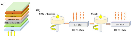
Figure 1.
(a) diagram of the device for inverted planar perovskite solar cells; (b) Schematic diagram of spining coating HTLs step.
Also Co2+ can increase the grain of perovskite film based on the same reasons. The radius of Co element is much bigger than Li, thus the phenomenon of pinhole will be more clear when the content of Co exceeds a certain concentration. Schematic diagram of solution spin coating NiOx HTL films at room temperature in this work is illustrated in Figure 1b. Four steps need to complete the fabrication process of the hole transport layer. The first step is that Li: NiOx or pure Li: NiOx solution was putted on the ITO. The second step is to anneal the above Li: NiOx or pure Li: NiOx layer film at 250 °C for 45 min. The third step is that the Co2+ solution was spined over Li: NiOx. The last step is to anneal the above film at 250 °C for 10 min. The perovskite film would be deposited as-prepared films with second method and then be annealed in the condition that the temperature of the hot plate is 105 °C. Heating time is 10 min (to improve the annealing effect, 40 uL IPA should be added during the annealing of the perovskite layer material).
From Figure 2a, the energy level of Li: NiOx (or Co: NiOx) is close to the energy level of MAIPbI3−xClx, which is quite beneficial to the transport of holes from perovskite layer to hole transport layer (HTL). The X-ray Diffraction (XRD) of perovskite layer based on the pristine NiOx and diverse doping concentration NiOx are showed in Figure 2b to demostrate Li+ and Co2+ doping NiOx can affect the crystal structure of the perovskite layer. Figure 2b showed the location of the diffraction peak of MAPbIxCl3−x films that was already annealed at 100 °C for 20 min. From Figure 2b, it can be observed that all the perovskite film based on different NiOx contained the diffraction peaks including three values with 14.21°, 28.51°, and 31.88° which is relative to (110), (220), and (310) lattice planes of the tetragonal perovskite structure respectively. It also can be obtained from Figure 2b that there is no 12.8° diffraction peaks (12.8° represents the diffraction peaks of the PbI2). Ihe effect of the perovskite layer on film formation not only has a better quality but also the crystallinity of MAPbIxCl3−x perovskite film stable in the condition of doping the element of Li, Co based on NiOx hole transport layer.
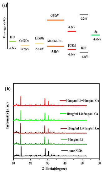
Figure 2.
(a) Energy level diagram of different layers of planar heterojunction perovskite solar cells; (b) XRD curve of perovskite film based on pristine NiOx, 10 mg/mL Li-doped NiOx, 10 mg/mL Li, 1 mg/mL Co-codoped NiOx, 10 mg/mL Li, 5 mg/mL Co-codoped NiOx, 10 mg/mL Li, 10 mg/mL Co-codoped NiOx.
Figure 3 is always showing the photo-current density–voltage (J–V) curves of the NiOx—based perovskite solar cells with different amounts of Li+, Co2+ doping, where marks different colors to distinguish different substances. The device performance of Voc, Jsc, FF and PCE with different Li, Co content are listed in Table 1. From J–V curve of the devices, it can be obviously obtained that doping NiOx with Li and Cu can improve the photoelectric conversion efficiency perovskite light absorbing layer. Figure 3b demostraed that the average performance parameter of the best device is PCE = (18.3 ± 0.3)%, Voc = (1.02 ± 0.01) V, FF(fill factor) = (0.73 ± 0.02) and Jsc = (20.8 ± 0.3) mA/cm2 respectively, which is obtained from the device based on 10 mg/mL Li, 5 mg/mL Co codoped NiOx. We achieved the peak PCE of 18.7% related to Voc = 1.06 V, Jsc = 21.7 mA/cm2 and FF = 0.75. Meanwhile, the PCE of the best solar cell devices based on pristine NiOx is 14.1% with open-circuit voltage Voc of 1.0 V, a short circuit current density Jsc of 20.09 mA/cm2 and a fill factor FF of 0.7 respectively. The device with 10 mg/mL Li-doped NiOx improved the performance of PSCs, with obtaining PCE = 14.79%, Jsc = 21.1 mA/cm2, Voc = 0.98 V, and FF = 0.71 respectively which are the best devices performance based on 10 mg/mL Li-doped NiOx. Similarly, the PSC device with 10 mg/mL Li, 1 mg/mL Co codoped NiOx obviously increase the PCE to (16.6 ± 0.5)%, the Jsc to (21.1 ± 0.5) mA/cm2, the Voc to (1.03 ± 0.02) V, corresponding to the FF = (0.69 ± 0.03). However, with the doping concentration of NiOx changing to 10 mg/mL Li and 5 mg/mL Co, the performance of the devices was worse with PCE = (12.6 ± 0.4)%, Jsc = (18.6 ± 0.6) mA/cm2, Voc = (0.85 ± 0.05) V, and FF = (0.57 ± 0.05).
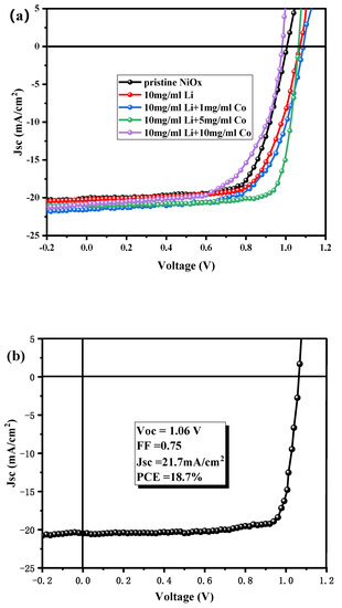
Figure 3.
(a) Current density (Jsc)–voltage (V) characteristics of perovskite solar cells for two-step method under standard test conditions (AM 1.5G, 100 mW cm−2) based on different doping content in NiOx; (b) J–V curve of the best device and corresponding device performance parameters.

Table 1.
Summarized photovoltaic performances of PSCs under AM 1.5G illumination (100 mW/cm2).
Figure 4 is to experiments hysteresis in device. The results showed there were negligible hysteresis for the PSCs based on pure NiOx, 10 mg/mL Li doped NiOx, 10 mg/mL Li, 1 mg/mL Co codoped NiOx, 10 mg/mL Li, 5 mg/mL Co codoped NiOx, which demonstrated that NiOx is a suitable and stable material of hole transport layer for perovskite solar cell. And NiOx is less expensive with little influence on stability of the devices. However, it can be seen from Figure 4e that there is much hysteresis in perovskite layer when the codoped concentration chaged to 10 mg/mL Li, 10 mg/mL Co, which lead to increase pinhole with too much Co element adding and then leading the quality of perovskite film decreased correspondingly.
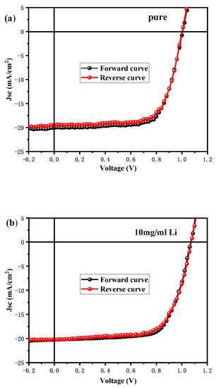
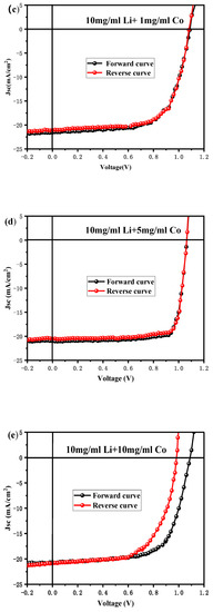
Figure 4.
Forward scan (−0.2 V → 1.2 V, step 0.08 V, delay time 500 ms) and Reverse scan (1.2 V → −0.2 V, step 0.08 V, delay time 500 ms) of Inverted planar heterojunction perovskite solar device with different Li, Co doping content. (a) pristine NiOx; (b) 10 mg/mL Li doped NiOx; (c) 10 mg/mL Li, 1 mg/mL Co codoped NiOx; (d) 10 mg/mL Li, 5 mg/mL Co codoped NiOx; (e) 10 mg/mL Li, 10 mg/mL Co codoped NiOx.
For investigating the perovskite layer absorption condition in the visible range, the IPCE along with the change of wavelength is depicted. From Figure 5a showed the value of IPCE (incident photon-to-electron conversion efficiency) has been improved much more with doping Li, Co into NiOx HTLs. The absorption strength was improved with doping Li, Co, and particularly had a visible improve with the value of 10 mg/mL Li, 5 mg/mL Co codoped in HTLs. However, when the codoped concentration changed to 10 mg/mL Li, 10 mg/mL Co, it can be observed obviously that IPCE value declined drastically, which may be owing to defects increasing in perovskite light absorbing layer film. The IPCE spectrum and integrated Jsc of the device is showed in Figure 5b. The integrated Jsc is 22.1 mA/cm2, which is basically consistent with the measured Jsc = 21.7 mA/cm2 value of the J–V curve and the corresponding IPCE has a broad plateau with a maximum value of 84.1% over essentially the entire visible range. Based on above results, the IPCE value of perovskite light absorbing layer varied a lot based on different NiOx HTL, especially for the device with 10 mg/mL Li, 5 mg/mL Co codoped NiOx.
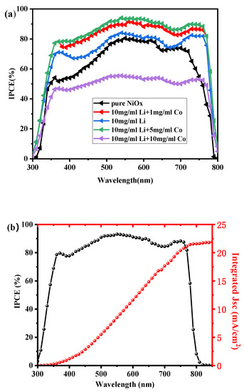
Figure 5.
(a) The IPCE spectrum of MAPbI3−xClx perovskite film based on different HTLs; (b) The IPCE spectrum (black) and integrated Jsc (red) of the best device.
Because the stability of device performance is an important criterion for measuring the quality of a device, the PCE curve with time of perovskite solar device based on different NiOx HTL was depicted in Figure 6a in an ambient environment (22 °C, 30% humidity). From the Figure 6a, compare with the PSCs based on pristine NiOx of, doping Li+ or Li+, Co2+ co-doped NiOx of PSCs showed better in stability of PSCs. The enhanced stability is for two reasons. The first is the crystal grains of perovskite film is much larger and denser in the process of Co infiltration into the perovskite layer. The second is that HTL can effectively block more the ambient air entering the perovskite layer.
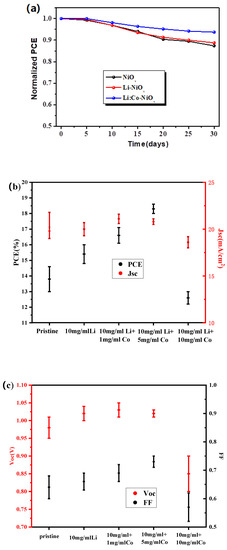
Figure 6.
(a) PCE change of the best PSCs with no doping, 10 mg/mL Li doping, 10 mg/mL Li and 1 mg/mL Co codoping, 10 mg/mL Li and 5 mg/mL Co codoping, 10 mg/mL Li and 10 mg/mL Co codoping; (b) PCE and Jsc values of PSCs in three batches with different doping degrees; (c) Voc and FF values of PSCs in three batches with different doping degrees.
To investigate the device reproducibility, experiments were conducted for each concentration. The PSCs with pristine NiOx had a seriously change while the PSCs based on Li+ or Li+, Co2+ codoping NiOx HTL appeared few distributions (Figure 6b,c).
In order to investigate the effect of Li and Co doping on the photophysics of MAPbIxCl3−x, the steady-state photoluminescence (PL) measurements were included. PL measurements were adopted to analyze the extraction efficiency of photogenerated carriers from perovskite layer to NiOx layer. Figure 7a showed that the PL quenching of MAPbIxCl3−x changed with different concentration of Li and Co doping in NiOx substrates. The effect of PL quenching without doping was remarkable that may be ascribe to the relatively small grains of perovskite. And it was weaken after doping 10 mg/mL Li+ in NiOx HTL and was more obvious with Co element doping in NiOx. Li+ and Co2+ can increase charge transfer rate from photoactive layer transport layer and cut down the recombination of photogenerated carriers. The UV-vis absorption spectra (Figure 7b) manifest Li, Co codoped in NiOx at lower concentrations cannot affect the perovskite thin film absorption (such as 10 mg/mL Li doped NiOx, 10 mg/mL Li, 1 mg/mL Co codoped NiOx, 10 mg/mL Li, 5 mg/mL Co codoped NiOx), but it may produce impediment effect the perovskite thin film absorption at higher content (such as 10 mg/mL Li, 10 mg/mL Co codoped NiOx).
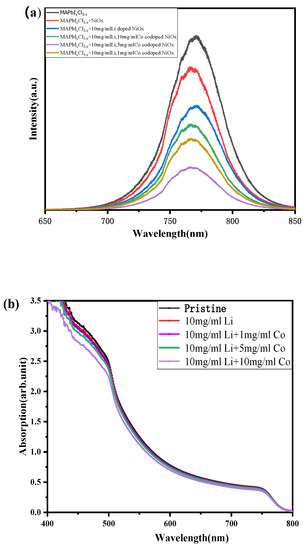
Figure 7.
(a) Photoluminescence of MAPbIxCl3−x which based on glass, pristine NiOx, 10 mg/mL Li doped NiOx, 10 mg/mL Li, 1 mg/mL Co codoped NiOx, 10 mg/mL Li, 5 mg/mL Co codoped NiOx, 10 mg/mL Li, 10 mg/mL Co codoped NiOx; (b) UV-vis absorption spectra based on different HTL.
The steady-state photocurrent output and PCE at maximum power point diagram as a function of time for the pristine device and the best device based on 10 mg/mL Li, 5 mg/mL Co codoped NiOx HTL were showed in Figure 8. The steady-state PCE output with 14.9% and 18.4% has been exhibited for conventional device and the best device respectively. It is demonstrated that the device performance are stable. And the absence of photocurrent hysteresis has been proved in the devices.
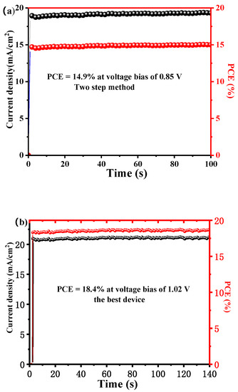
Figure 8.
The steady state outputs of current density and PCE at maximum. (a) the conventional device using two step method based on pure NiOx; (b) the best device based on 10 mg/mL Li, 5 mg/mL Co codoped NiOx.
3. Conclusions
In conclusion, the influence of Li, Co-codoped NiOx to the photovoltaic performance of PSSc was experimented. In this paper, one step method which is simple and effective was used and the elements of Li and Co are also non-poisonous and no impact on the stability of the PSSc. The influence of Li doping NiOx is that can evidently improve the fill factor(FF) of PSSc while can increase the grain size of the perovskite film. The improvement of FF, which is a greatly significant characteristic of PSSc, is caused by the increased electrical conductivity. The p-type Co2+ was first doped into a NiOx using spin coating at room-temperature and then was heated at a low temperature (about 250 °C) with the purpose of heating to make Co2+ element better to enter the perovskite layer. The film adding Co2+ made a great promotion of hole mobility in a way meanwhile made the surface of the perovskire layer more smoother. According to the report, a low doping degree of Li+ can increase the Jsc and FF, and increase the PCE of PSCs. Optimal doping is 10 mg/mL Li, 5 mg/mL Co, the Jsc increasing from 20.09 mA/cm2 to 21.7 mA/cm2, the FF increasing from 0.7 to 0.75, and the PCE similarly from14.1% to 18.7%. The experimental results and mechanism analysis suggest that Li, Co doping NiOx is really a promising way to improve the photovoltaic performance of PSCs.
All the materials including nickel acetate (Ni(CH3COO)2 4H2O), Methylammonium iodide (CH3NH3I, 99.9%, Dyesol), Co(3)TFSI, LiTFSI, acetonitrile, Decon-90 cleaning agent, deionized water, acetone, alcohol, lead (II) iodide (PbI2, 99.999%, Alfa), lead (II) chloride (PbCl2, 99.999%, Alfa), phenyl-C61-butyric acid methyl ester (PC61BM, 98%, nano-c), chlorobenzenes (99.8%, Sigma), isopropanol (99.5%, Sigma), and bathocuproine (96%, Alfa), Dimethyl sulphoxide(DMSO, 99.8%), γ-hydroxybutyrate lactone (GBL), N,N′-dimethylformamide (DMF, 99.8%, Aladdin), Ag (electrode material), were used as received without further purification.
For the sol–gel-processed NiOx, 248.8 mg Ni(CH3COO)2·4H2O (1.0 mmol) with 60 µL (0.001 mmol) ethanolamine was dissolved in 2-methoxyethanol (10 mL). Then, the solution was stirred at 70 °C for 4 h.
The patterned ITO glass substrates were sequentially ultrasonic cleaned with detergent, de-ionized water, acetone, and isopropyl alcohol at 50 °C for 20 min, respectively. Inverted planar PSCs were fabricated on pre-patterned ITO glass substrates (around 2 × 2.5 cm2 in size, 10 Ω per square). Then, after a thin layer of NiOx or Li-NiOx was spin-coated on the substrates at 3000 rpm for 42 s and annealed at 250 °C for 35 min, the ITO substrates were dried with nitrogen gun and treated in a UV ozone oven for 15 min. After that the substrates were transferred into a nitrogen-filled glovebox. The spin-coating process of the Co(3)TFSI solution was programmed to run at 3000 rpm for 45 s and then annealed at 250 °C for 10 min. A MAPbI3−xClx precursor solution containing 1.26 M PbI2, 0.14 M PbCl2 and 1.35 M MAI was prepared in the cosolvent of DMSO:GBL (3:7 vol. ratio), and stirred for 2 h at 75 °C. The spin-coating process for the perovskite precursor solution was programmed to run at 1000 rpm for 20 s and then 4000 rpm for 40 s. When the spinning was at 50 s, 350 μL anhydrous chlorobenzene solution was injected onto the substrates that had. The perovskite films were thermally annealed on the hotplate at 100 °C for 20 min. Then, a layer of PCBM (20 mg mL−1 in chlorobenzene) was spin coated on the top of the perovskite layer at 2000 rpm for 40 s. After that, a thin layer of BCP (0.5 mg mL−1 in IPA) was spin coated on the top of the PCBM layer. The devices were achieved by thermally evaporated 100 nm Ag in high vacuum (≤5 × 10⁻⁴ Pa) through a shadow mask. All the devices had an area of 7 mm2.
The UV-visible absorption spectra were recorded with an UV-visible spectrophotometer (Perkin-Elmer Lambda 950) (PerkinElmer, Boston, MA, USA). The X-ray diffraction (XRD) test was conducted on Bruker D8 Advance XRD. Photovoltaic performances were measured by using a Keithley 2400 source meter under simulated sunlight from XES-70S1 solar simulator matching the AM 1.5G standard with an intensity of 100 mW/cm2. Incident photo-to-current conversion efficiencies (IPCEs) of PSCs were tested by the solar cell quantum efficiency measurement system (SCS10-X150, Zolix Instruments Co. Ltd., Beijing, China). The system was calibrated against a NREL certified silicon reference solar cell. All the measurements were carried under ambient atmosphere at room temperature without encapsulation. We use Tektronix D4105 (A digital oscilloscope) to record the photocurrent or photovoltage decay process with a sampling resistor of 50 Ω or 1 MΩ, respectively.
Author Contributions
For research articles with several authors, a short paragraph specifying their individual contributions must be provided. The following statements should be used Conceptualization, C.Z.; methodology, H.G.; software, Y.Y.; validation, Y.Y., S.W.; formal analysis, S.W.; data curation, Y.Y.; writing—original draft preparation, S.W.; writing—review and editing, S.W.; visualization, Y.Y.; supervision, H.G.; project administration, C.Z.; funding acquisition, S.W. All authors have read and agreed to the published version of the manuscript.
Funding
This research was funded by Key Research and Development Program of Shaanxi Province, grant number 2018GY-006 and 2020GY-097, Youth Program of National Natural Science Foundation, grant number 61804126, Technology Development Program of Taicang, grant number, TC2019DYDS07) and Technology Development Program founding of xi’an, grand number, 201805042YD 20CG26.
Conflicts of Interest
The authors declare no conflict of interest.
References
- Becquerel, A.E. Photoelctrochemical effect. CR Acad. Sci. Paris 1839, 9, 14. [Google Scholar]
- Yin, W.J.; Shi, T.; Yan, Y. Unique properties of halide perovskites as possible origins of the superior solar cell performance. Adv. Mater. 2014, 26, 4653–4658. [Google Scholar] [CrossRef] [PubMed]
- Shi, D.; Adinolfi, V.; Comin, R.; Yuan, M.J.; Alarousu, E.; Buin, A.; Chen, Y.; Hoogland, S.; Rothenberger, A.; Katsiev, K.; et al. Low trap-state density and long carrier diffusion in organolead trihalide perovskite single crystals. Science 2015, 347, 519–522. [Google Scholar] [CrossRef] [PubMed]
- Miyata, A.; Mitioglu, A.; Plochocka, P.; Portugall, O.; Wang, J.T.-W.; Stranks, S.D.; Snaith, H.J.; Nicholas, R.J. Direct measurement of the exciton binding energy and effective masses for charge carriers in organic-inorganic tri-halide perovskites. Nat. Phys. 2015, 11, 582–587. [Google Scholar] [CrossRef]
- Stranks, S.D.; Eperon, G.E.; Grancini, G.; Menelaou, C.; Alcocer, M.J.P.; Leijtens, T.; Herz, L.M.; Petrozza, A.; Snaith, H.J. Electron-hole diffusion lengths exceeding 1 micrometer in an organometal trihalide perovskite absorber. Science 2013, 342, 341–344. [Google Scholar] [CrossRef]
- Park, N.G.; Grätzel, M.; Miyasaka, T. Organic-Inorganic Halide Perovskite Photovoltaics; Springer International Publishing: Basel, Switzerland, 2016. [Google Scholar]
- Available online: https://www.nrel.gov/pv/assets/pdfs/best-research-cell-efficiencies.20190802.pdf (accessed on 2 August 2019).
- Nie, W.; Tsai, H.; Asadpour, R.; Blancon, J.-C.; Neukirch, A.J.; Gupta, G.; Crochet, J.J.; Chhowalla, M.; Tretiak, S.; Alam, M.A. Solar cells. High-efficiency solution-processed perovskite solar cells with millimeter-scale grains. Science 2015, 347, 522–525. [Google Scholar] [CrossRef]
- Shao, Y.; Yuan, Y.B.; Huang, J. Correlation of energy disorder and open circuit voltage in hybrid perovskite solar cells. Nat. Energy 2016, 1, 15001. [Google Scholar] [CrossRef]
- Kim, H.S.; Morasero, I.; Gonzalezpedro, V.; Fabregatsantiago, F.; Juarezperez, E.J.; Park, N.G.; Bisquert, J. Mechanism of carrier accumulation in perovskite thin-absorber solar cells. Nat. Commun. 2013, 4, 2242. [Google Scholar] [CrossRef]
- Li, H.; Fu, K.; Boix, P.P.; Wong, L.H.; Hagfeldt, A.; Grätzel, M.; Mhaisalkar, S.G.; Grimsdale, A.C. Hole-transporting small molecules based on thiophene cores for high efficiency perovskite solar cells. ChemsusChem 2014, 7, 3420. [Google Scholar] [CrossRef]
- Yu, Z.; Sun, L. Recent progress on hole transporting materials for emerging organometal halide perovskite solar cells. Adv. Energy Mater. 2015, 5, 1500213. [Google Scholar] [CrossRef]
- Liu, J.; Wu, Y.; Qin, C.; Yang, X.; Yasuda, T.; Islam, A.; Zhang, K.; Peng, W.; Chen, W.; Han, L. A dopant free hole transporting material for efficient and stable perovskite solar cells. Energy Environ. Sci. 2014, 7, 2963–2967. [Google Scholar] [CrossRef]
- Jin, H.H.; Sang, H.I.; Noh, J.H.; Mandal, T.N.; Lim, C.S.; Chang, J.A.; Yong, H.L.; Kim, H.J.; Sarkar, A.; Nazeeruddin, M.K. Efficient inorganic organic hybrid heterojunction solar cells containing perovskite compound and polymeric hole conductors. Nat. Photonics 2013, 7, 486–491. [Google Scholar]
- Jeon, N.J.; Noh, J.H.; Kim, Y.C.; Yang, W.S.; Ryu, S.; Seok, S.I. Solvent engineering for high performance inorganic organic hybrid perovskite solar cells. Nat. Mater. 2014, 13, 897. [Google Scholar] [CrossRef] [PubMed]
- Heo, J.H.; Im, S.H.; Noh, J.H.; Mandal, T.N.; Lim, C.-S.; Chang, J.A.; Lee, Y.H.; Kim, H.J.; Sarkar, A.; Nazeeruddin, M.K. Photoenergy and Thin Film Materials. Nat. Photonics 2013, 7, 486–491. [Google Scholar] [CrossRef]
- Malinkiewicz, O.; Yella, A.; Yong, H.L.; Espallargas, G.M.; Graetzel, M.; Nazeeruddin, M.K.; Bolink, H.J. Perovskite solar cells emplying organic charge transport layers. Nat. Photonics 2014, 8, 128–132. [Google Scholar] [CrossRef]
- Qin, P.; Tanaka, S.; Ito, S.; Tetreault, N.; Manabe, K.; Nishino, H.; Nazeeruddin, M.K.; Grätzel, M. Inorganic hole conductor based lead halide perovskite solar cells with 12.4% conversion efficiency. Nat. Commun. 2014, 5, 3834. [Google Scholar] [CrossRef]
- Wang, Z.K.; Li, M.; Yuan, D.X.; Shi, X.B.; Ma, H.; Liao, L.S. Planar perovskite solar cells with 15.75% power conversion efficiency by cathode and anode interfacial modification. ACS Appl. Mater. Interfaces 2015, 7, 9645. [Google Scholar] [CrossRef]
- Hu, L.; Wang, W.; Liu, H.; Peng, J.; Cao, H.; Shao, G.; Xia, Z.; Ma, W.; Tang, J. A room-temperature CuAlO2 hole interfacial layer for efficient and stable planar perovskite solar cells. J. Mater. Chem. A 2015, 3, 515–518. [Google Scholar] [CrossRef]
- della Gaspera, E.; Peng, Y.; Hou, Q.; Spiccia, L.; Bach, U.; Jasieniak, J.J.; Cheng, Y.-B. Search ResultsWeb resultsUltra-thin high efficiency semitransparent perovskite solar cells. Nano Energy 2015, 13, 249–257. [Google Scholar] [CrossRef]
- Hou, F.; Su, Z.; Jin, F.; Yan, X.; Wang, L.; Zhao, H.; Zhu, J.; Chu, B.; Li, W. Efficient and stable planar heterojunction perovskite solar cells with an MoO3/PEDOT:PSS hole transporting layer. Nanoscale 2015, 7, 9427–9432. [Google Scholar] [CrossRef]
- You, J.; Meng, L.; Song, T.-B.; Guo, T.-F.; Yang, Y.; Chang, W.-H.; Hong, Z.; Chen, H.; Zhou, H.; Chen, Q.; et al. Improved air stability of perovskite solar cells via exsitu solution processed metal oxide transport layers. Nat. Nanotechnol. 2016, 11, 75–81. [Google Scholar] [CrossRef] [PubMed]
- Zhu, Z.; Bai, Y.; Zhang, T.; Liu, Z.; Long, X.; Wei, Z.; Wang, Z.; Zhang, L.; Wang, J.; Yan, F.; et al. High-performance hole extraction layer of sol-gel-processed NiO nanocrystals for inverted planner perovskite soclar cells. Angew. Chem. Int. Ed. 2014, 126, 12779–12783. [Google Scholar] [CrossRef]
- Subbiah, A.S.; Halder, A.; Ghosh, S.; Mahuli, N.; Hodes, G.; Sarkar, S.K. Inorganic Hole Conducting Layers for Perovskite-Based Solar Cells. J. Phys. Chem. Lett. 2014, 5, 1748–1753. [Google Scholar] [CrossRef] [PubMed]
- Burschka, J.; Pellet, N.; Moon, S.-J.; Humphry-Baker, R.; Gao, P.; Nazeeruddin, M.K.; Gr-tzel, M. Sequential deposition as a route to high-performance perovskite-sensitized solar cells. Nature 2013, 499, 316–319. [Google Scholar] [CrossRef] [PubMed]
- Tiwana, P.; Docampo, P.; Johnston, M.B.; Snaith, H.J.; Herz, L.M. Electron Mobility and Injection Dynamics in Mesoporous ZnO, SnO2, and TiO2 Films Used in Dye-Sensitized Solar Cells. ACS Nano 2011, 5, 5158–5166. [Google Scholar] [CrossRef]
- Snaith, H.J.; Ducati, C. SnO2-Based Dye-Sensitized Hybrid Solar Cells Exhibiting Near Unity Absorbed Photon-to-Electron Conversion Efficiency. Nano Lett. 2010, 10, 1259–1265. [Google Scholar] [CrossRef]
- Baena, J.P.C.; Steier, L.; Tress, W.; Saliba, M.; Neutzner, S.; Matsui, T.; Giordano, F.; Jacobsson, T.J.; Kandada, A.R.S.; Zakeeruddin, S.M.; et al. Highly Efficient Planar Perovskite Solar Cells through Band Alignment Engineering. Energy Environ. Sci. 2015, 8, 2928–2934. [Google Scholar] [CrossRef]
- Kumari, N.; Patel, S.R.; Gohel, J.V. Current Progress and Future Prespective of Perovskite Solar Cells: A Comprehensive Review. Rev. Adv. Mater. Sci. 2018, 53, 161–186. [Google Scholar] [CrossRef]
- Xia, X.F.; Jiang, Y.H.; Wan, Q.X. Lithium and Silver Co-Doped Nickel Oxide Hole Transporting Layer Boosting the Efficiency and Stability of Inverted Planar Perovskite Solar Cells. ACS Appl. Mater. Interfaces 2018, 10, 44501–44510. [Google Scholar] [CrossRef]


© 2020 by the authors. Licensee MDPI, Basel, Switzerland. This article is an open access article distributed under the terms and conditions of the Creative Commons Attribution (CC BY) license (http://creativecommons.org/licenses/by/4.0/).