Article

Experimental Investigation of Thermal Annealing and Ferroelectric Capacitor Area Effects for Hafnium-Zirconium Oxide Devices

Department of Materials & Mineral Resources Engineering, National Taipei University of Technology, Taipei 10608, Taiwan
*
Author to whom correspondence should be addressed.
Coatings 2020, 10(8), 733; https://doi.org/10.3390/coatings10080733
Submission received: 4 July 2020 / Revised: 23 July 2020 / Accepted: 24 July 2020 / Published: 26 July 2020

Abstract

:
In this study, we reveal that the thermal budget of post-metal annealing not only determines the formation of the ferroelectric phase and dipole domain but also the film quality of the gate stack in a metal-ferroelectric-metal capacitor. The higher leakage current caused by defect traps or grain boundaries within a gate stack would influence the stability of the ferroelectric domain switching. Furthermore, the ferroelectric domain switching and polarization current also depend on the ferroelectric capacitor area. We observe that a HfAlO ferroelectric capacitor can dominate the transfer characteristics of a p-type SnO thin-film transistor through the modulation of series capacitance in the gate stack based on a one-transistor one-capacitor series configuration. According to experimental results, the memory hysteresis window can be improved significantly with the area scaling due to the improvement of capacitance matching accuracy.

1. Introduction

Recently, the research for the ferroelectric-based transistor materials has been focused on the polycrystalline-doped hafnium oxide (HfO2) due to good thickness scalability and complementary metal oxide semiconductor (CMOS) process compatibility. Since the discovery of ferroelectricity in HfO2 material, the HfO2-based ferroelectric transistors and memories have been considered as one of the most promising candidates to replace the conventional perovskite structure, such as PbZrTiO3 (PZT) and strontium bismuth tantalite (SBT) [1]. These novel HfO2-based ferroelectric materials and related devices exhibit fast switching speed, low power consumption, high scalability and long-endurance cycling [2,3,4]. The related negative capacitor effect for reducing the switching power of the transistor also attracts more and more attention [5,6]. Such numerous advantages show a great potential for the applications of volatile memory, nonvolatile memory (NVM) and logic devices. In recent years, the novel ferroelectric memories using HfZrOx (HZO) with zirconium doping have been reported and investigated, frequently owing to the outstanding hysteresis polarization effect and extensive process rangeability of doping concentration [7]. Although the HZO ferroelectric memory has the advantages of good device scalability and a fast switching speed of sub-100ns, the poor thermal stability of Zr doping, the leakage current issue and the small ferroelectric hysteresis window are the major concerns with the thickness scaling [8,9,10,11,12,13,14,15]. As for another ferroelectric material of HfAlOx with a light Al doping concentration (<10%), the leakage current can be improved due to the large bandgap of AlOx. However, the hysteresis window modulation still faces a big challenge due to the limitation of Al doping concentration [16,17].
The advantages of metal-oxide-based thin-film transistors (TFTs) over the silicon-based TFTs include good transparency, reasonably high carrier mobility and a relatively low processing temperature. In recent years, the metal-oxide-based TFTs have been actively pursued for displays and other new applications [18,19]. Although the hysteresis in transistors is undesirable in most circuit application, it has been exploited to realize electronic memory elements due to the remnant polarization (Pr). According to the type of the hysteresis, different memories based on oxide TFTs have been reported. For the TFT-based ferroelectric hysteresis memory, one-transistor (1T) TFTs that use ferroelectric polymer materials as the gate insulator have been proposed and investigated [20,21]. For the trapping hysteresis, an NVM has been fabricated using a ZnO TFT with Ag nanoparticles embedded as charge storage nodes at the insulator–ZnO interface [22]. We have previously proposed high-performance tin oxide (SnO) TFTs for display application [23,24,25]. In this work, we fabricated one transistor and one capacitor (1T-1C) device structure integrating a p-type SnO TFT and a ferroelectric HfZrO capacitor and investigated the influence of the thermal annealing and capacitor area. The optimized characteristics include an on/off state current ratio (ION/IOFF) of >103 and a larger memory window of 6 V under an operating voltage of 6.5 V, which can be ascribed to the optimal capacitance matching and less defect-induced leakage current.

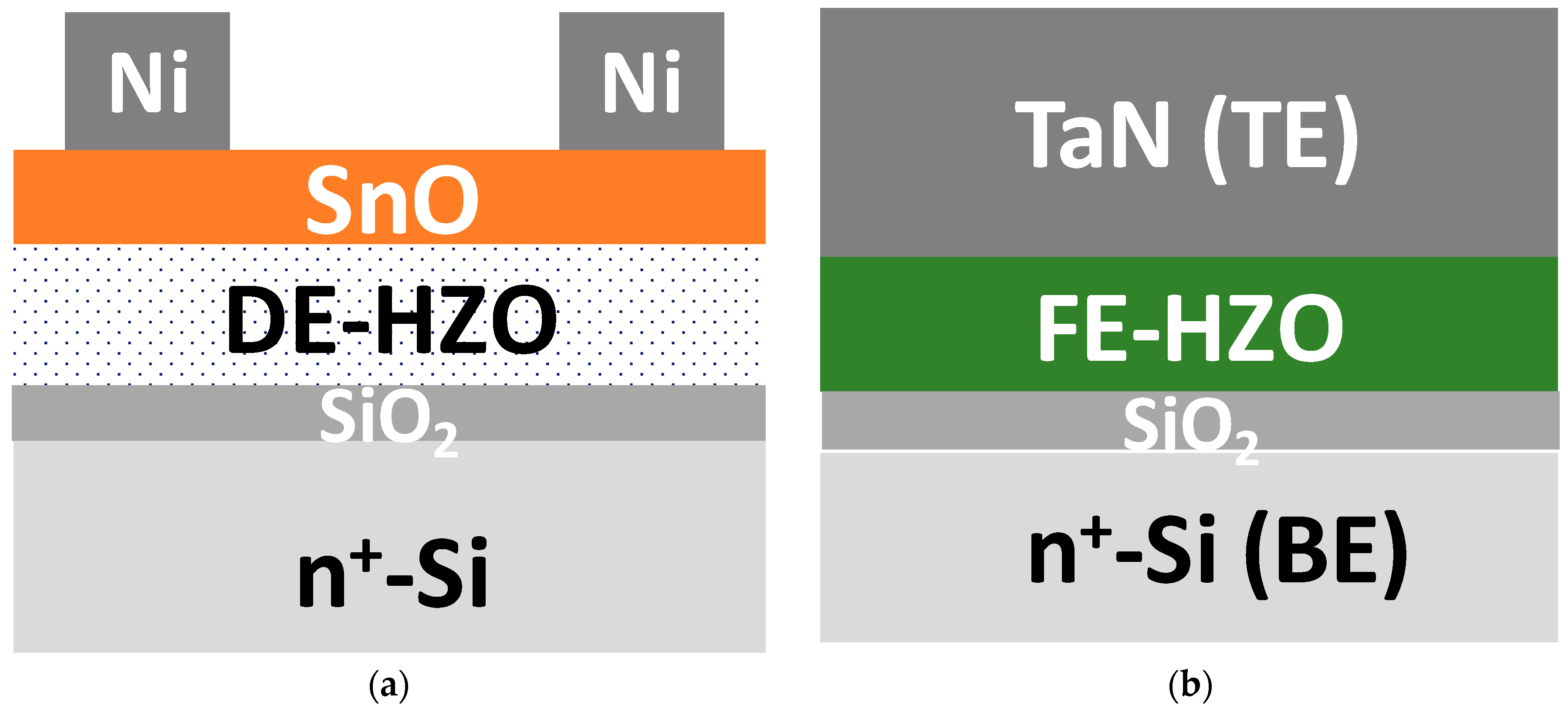
2. Materials and Methods

First, the fabrication process of the p-type SnO TFT and ferroelectric MFM capacitor was described as the following. For the ferroelectric HZO (FE HZO) MFM capacitor, a highly doped N+-type silicon wafer was used as a bottom electrode. To avoid the silicon interface reaction during annealing, a 1-nm-thick silicon dioxide buffer layer was deposited. Then, a 10-nm-thick HfZrO film with an optimized zirconium concentration of 25% [26] was deposited on the buffer oxide by an atomic layer deposition (ALD) system. Finally, the tantalum nitride (TaN) gate was deposited on the HZO film by sputtering physical vapor deposition and then followed by a post-metal annealing (PMA) to enhance the ferroelectric phase transition [26,27]. The dielectric HZO (DE-HZO) film deposited by ALD can be transformed from tetragonal phase to orthorhombic phase by TaN metal capping. The Figure 1a,b show the transmission electron microscope (TEM, JEOL, Tokyo, Japan) and fast fourier transform (FFT) images of 10-nm-thick HZO film. The geometric phase analysis (GPA) images for x and y strain planes simulated from TEM images are shown in the Figure 1c,d. From the GPA results, we can observe the difference of strain field along x and y axis caused by ferroelectric phase transition during annealing, which is important for TaN gate stress engineering.
To investigate the ferroelectric polarization and capacitance matching effect of an MFM capacitor, the different capacitor areas were designed. The MFM capacitors were patterned by photolithography with different areas. For the fabrication process of the p-type SnO TFT, we also adopted the highly-doped N+-Si substrate as the bottom gate electrode. Next, a 1-nm-thick buffer oxide and a 10-nm-thick DE HZO layer with 25% zirconium doping were grown. Subsequently, a 6-nm-thick SnO was grown as the active channel layer, followed by a 200 °C annealing and fluorine plasma treatment [28]. Finally, a 50-nm-thick Ni metal was deposited as the source and drain contact electrodes by sputtering. The p-type SnO TFT device has a channel width of 500 μm and a channel length of 50 μm. The schematic device structures of the p-type SnO TFT using DE-HZ film as gate dielectric and a ferroelectric FE-HZO MFM capacitor were shown in Figure 2a,b. The electrical properties and memory characteristics of an MFM capacitor and TFT-based memory with 1T-1C series-connection design were simultaneously measured for clarifying the mechanism of ferroelectric domain switching and the impact on the memory performance of 1T-1C device structure under annealing temperature and area effect.

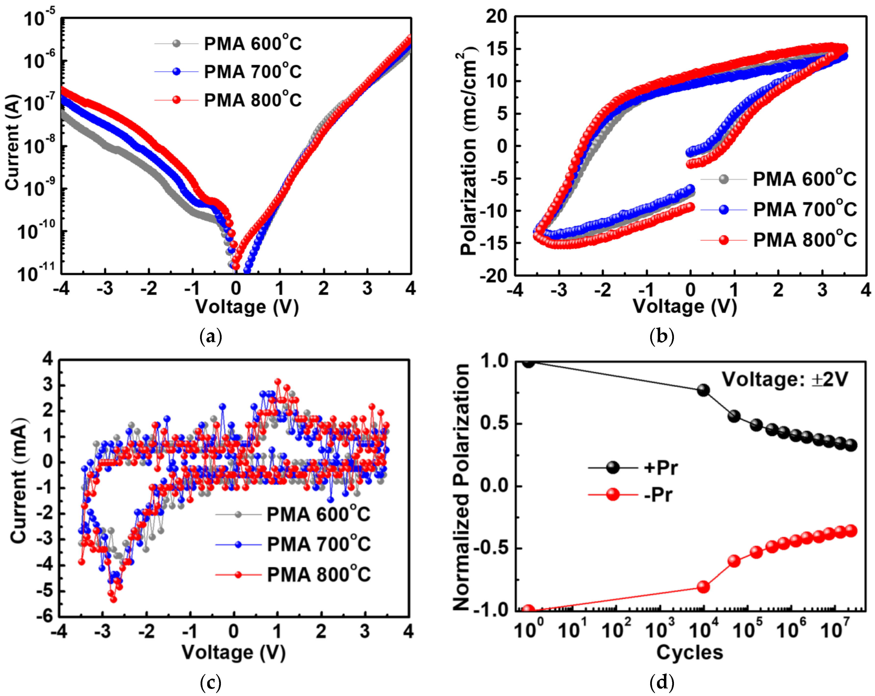
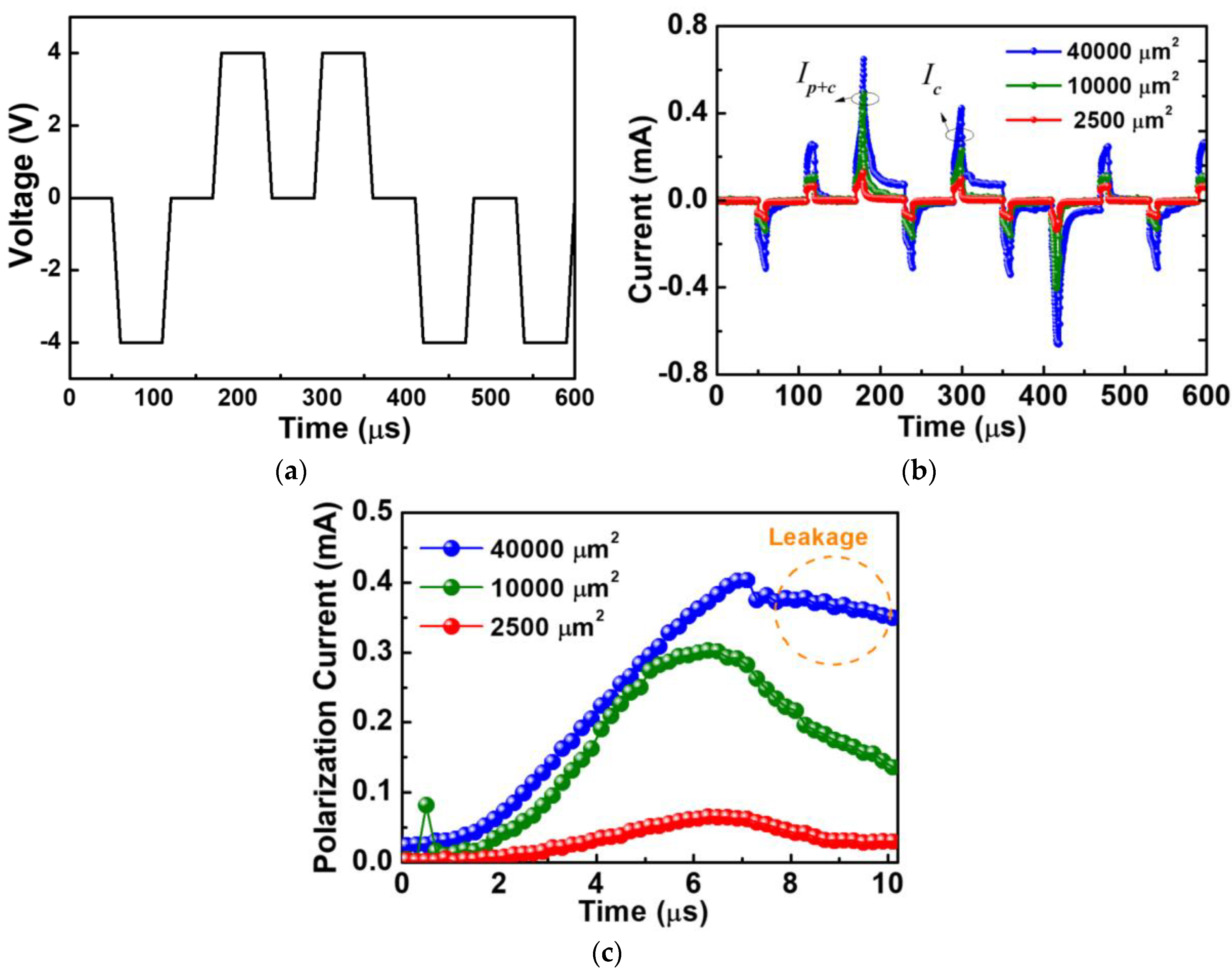
3. Results and Discussion

Figure 3a shows the current–voltage curves of HZO MFM capacitors at various PMA temperature conditions. We can clearly observe that the leakage current has no significant change in the positive bias side but presents the temperature dependence of a leakage current in the negative bias side. This small leakage variation in the positive bias side can be ascribed to the thermally stable SiO2 interface buffer layer with a large band gap, which is favorable to reduce the defect generation during the PMA process and thus suppress the leakage current. However, the increased leakage current with a PMA temperature measured at the negative bias side with electron gate injection is highly correlated with interface quality between the stressed TaN gate and HZO film [11]. We believe that the temperature-induced leakage current is mainly contributed to by interface defects near TaN gate and grain boundaries. Figure 3b,c presents the hysteresis polarization (P-V) loops and the instantaneous currents of HZO MFM capacitors under PMA temperatures from 600 to 800 °C. The ferroelectricity of HZO film gradually enhances with the increase in the annealing temperature from 600 to 800 °C. However, we also find the slightly higher leakage current at 800 °C, which can be ascribed to the increase in defects or leakage paths in the gate stack due to the change of grain size [12]. Figure 3d shows the endurance cycling characteristic of HZO MFM capacitor with optimal PMA condition of 700 °C. We can clearly observe that the ferroelectric MFM capacitor can be stably switched up to 107 cycles under a low bias condition of 2 V. The stable endurance property and low voltage operating are important for the development and application of low-power memory.
To further characterize the ferroelectric properties of the HZO capacitor, the PUND (positive up negative down) measurement was performed [13]. Figure 4a,b shows the PUND pulse waveform and output response current results for the HZO capacitors with different areas. The principle of PUND measurement is composed of a preset pulse, followed by two positive and two negative consecutive pulses. The negative preset pulse is utilized to activate the polarization before double pulse measurement [29]. Therefore, the current peak of Ip + c represents both the polarization switching and capacitor charging currents. However, the current peak of Ic only includes the capacitor charging current, since no polarization occurs during the second positive pulse. Thus, the polarization current (Ip) can be estimated from the difference between Ip + c and Ic, according to the equation:
I p = I p   +   c I c
To ensure that the HZO capacitor was fully polarized and prevent the leakage current, the switching voltage, holding time and rising time were set as ±4 V, 50 and 10 μs, respectively. Figure 4c shows the calculated polarization current for the HZO capacitors with different device areas. The ferroelectricity in the HZO capacitors was confirmed. According to Equation (1), the polarization currents of the HZO capacitors with the areas of 40,000, 10,000 and 2500 μm2 were 0.4, 0.3 and 0.065 mA, respectively, indicating that the HZO capacitor with a larger area exhibits the stronger polarization. The larger area the capacitor has, the more ferroelectric dipoles show up, resulting in the larger polarization current. However, the HZO capacitor with a large area of 40,000 μm2 also suffers from the leakage issue due to the existence of more defect traps. Therefore, the large polarization current also contains the contribution of a leakage-oriented component [14], which can significantly affect the ferroelectric domain switching, especially under the operation environment of high electric field or high temperature.
Figure 5 shows the typical transfer drain current versus gate voltage (ID-VG) curves of the p-type SnO TFT in the swept mode. The ION/IOFF ratio of the p-type SnO TFT shows 3 orders (~2 × 10³) of magnitude in the ID-VG curve, and the on-state and off-state currents are 2.8 × 10⁻⁶ A and 1.3 × 10⁻⁹ A at VD = −1 V, respectively. It was observed that the hysteresis for the ID-VG curves under the forward and reverse sweep is in the counterclockwise direction with a negative shift. This hysteresis phenomenon can be ascribed to the trap defects near the SnO channel. It is well known that this charge trapping effect is correlated with the interface quality between a vacancy-rich p-type SnO channel and a polycrystalline HZO gate dielectric [24], which affects the transfer characteristic of the p-type TFT.
Figure 6a is the schematic plot of 1T-IC series configuration. Figure 6b shows the transfer ID-VG curves of the 1T-1C device structure after integrating the ferroelectric HfZrO capacitor and p-type SnO TFT. From the measured ID-VG curves, the clockwise hysteresis with a positive shift was obviously observed, which was different from the ID-VG curves featuring a counterclockwise trapping hysteresis of the p-type SnO TFT device. This difference in electrical behaviour could be ascribed to the contribution of stronger ferroelectric domain dipoles in the FE-HZO MFM capacitor. Besides, due to the effect of series capacitance, the threshold voltage (VT) was larger than that of the original p-type SnO TFT device. Figure 6c shows the extracted memory window and ION/IOFF ratio at VG = −0.2 V as a function of the ferroelectric capacitor area. When decreasing the ferroelectric capacitor area from 40,000 to 2500 μm2, the memory window is apparently improved by 1.7 times from 3.5 to 6 V and the ION/IOFF ratio is also increased by 2.6 times from 196 to 500. Therefore, we can understand that both the memory window and ION/IOFF ratio can be improved significantly with the area scaling of ferroelectric capacitor. This is because the defects in the gate stack of FE-HZO/SiO2 is gradually reduced with the area scaling of the MFM capacitor and thereby the gate leakage is effectively suppressed in the smallest area condition of 2500 μm2. Figure 6d shows the ION/IOFF ratio as a function of reading time for the SnO TFT in series configuration with different HZO capacitor areas. We can also clearly observe that the smallest area condition of 2500 μm2 with a larger ION/IOFF ratio has a better data retention capability compared to other conditions. This is because the leakage current is correspondingly lower in the smallest area due to less leakage contribution from defect traps of HZO gate stack. Thus, adopting a small MFM area for the integration with the p-type TFT, the nanoscale domain dipoles in a low-leakage HZO film stack can be switched more effectively under the operation of high electric field.
Compared to 1T TFT-based ferroelectric memories [20,21] using ferroelectric polymer P(VDF-TrFE) materials featuring a thick-film thickness of 200 nm and a large operating voltage range from 30 to 60 V, our TFT-based ferroelectric memory using 1T-1C series configuration using a correspondingly thin 10-nm-thick HZO film shows the potential on the aspects of thick-film scaling and process integration with modern semiconductor manufacturing technology. Most importantly, the low operating voltage of 6 V is at least five times lower than those of 1T TFT-based ferroelectric polymer memories mentioned above.

4. Conclusions

In this work, the ferroelectric polarization behaviors of HZO MFM capacitors are compressively investigated under the consideration of various post-metal annealing temperatures and capacitor areas. The best ferroelectric performance of an HZO MFM capacitor can be achieved at a PMA condition of 700 °C under the considerations of ferroelectric polarization and memory operation characteristics. Under the design of 1T-1C series configuration, the ION/IOFF ratio of a p-type TFT can be further enhanced with capacitor area scaling due to the defect reduction of the gate stack and the improvement of the gate leakage current. Apparently, the smallest area condition of 2500 μm2 with a larger ION/IOFF ratio shows a better data retention capability compared to other area conditions. Furthermore, the memory windows in the range from 3.5 to 6 V can also be appropriately modulated by capacitor areas to gain a better series capacitance matching between the DE-HZO of a p-type SnO TFT and the FE-HZO of an MFM capacitor. Thus, the optimization of PMA and the device area of an MFM capacitor is necessary and beneficial for effectively improving the memory switching characteristics of TFT-based ferroelectric memory with 1T-1C series configuration.

Author Contributions

Conceptualization and methodology, H.-H.H.; validation and data curation, H.-M.L. and S.L.; writing—review and editing, H.-H.H.; supervision and project administration, H.-H.H. All authors have read and agreed to the published version of the manuscript.

Funding

This research was funded by the Ministry of Science and Technology, R.O.C., Grant No. MOST 107-2221-E-027 -060 -MY2.

Acknowledgments

The authors would like to thank the Ministry of Science and Technology (MOST) in Taiwan for financial supports and National Nano Device Laboratories for experimental supports.

Conflicts of Interest

The authors declare no conflict of interest.

References

  1. Yurchuk, E.; Muller, J.; Muller, S.; Paul, J.; Pesic, M.; van Bentum, R.; Schroeder, U.; Mikolajick, T. Charge-trapping phenomena in HfO2-based FeFET-type nonvolatile memories. IEEE Trans. Electron Dev. 2016, 63, 3501–3507. [Google Scholar] [CrossRef]
  2. Müller, J.; Yurchuk, E.; Schlosser, T.; Paul, J.; Hoffmann, R.; Muller, S.; Martin, D.; Slesazeck, S.; Polakowski, P.; Sundqvist, J.; et al. Ferroelectricity in HfO2 enables nonvolatile data storage in 28 nm HKMG. In Proceedings of the 2012 Symposium on VLSI Technology (VLSIT), Honolulu, HI, USA, 12–14 June 2010; pp. 25–26. [Google Scholar]
  3. Trentzsch, M.; Flachowsky, S.; Richter, R.; Paul, J.; Reimer, B.; Utess, D.; Jansen, S.; Mulaosmanovic, H.; Müller, J.; Slesazeck, S.; et al. A 28 nm HKMG super low power embedded NVM technology based on ferroelectric FETs. In Proceedings of the 2016 IEEE International Electron Devices Meeting (IEDM), San Francisco, CA, USA, 3–7 December 2016; pp. 11.5.1–11.5.4. [Google Scholar]
  4. Chen, K.T.; Chou, Y.C.; Siang, G.Y.; Chen, H.Y.; Lo, C.; Liao, C.Y.; Chang, S.T.; Lee, M.H. Evaluation of sweep modes for switch response on ferroelectric negative-capacitance FETs. Appl. Phys. Expr. 2019, 12, 071003. [Google Scholar] [CrossRef]
  5. Fan, C.C.; Cheng, C.H.; Chen, Y.R.; Liu, C.; Chang, C.Y. Energy-efficient HfAlOx NCFET: Using gate strain and defect passivation to realize nearly hysteresis- free sub-25mV/dec switch with ultralow leakage. In Proceedings of the International Electron Devices Meeting (IEDM), San Francisco, CA, USA, 2–6 December 2017; pp. 561–564. [Google Scholar]
  6. Mueller, S.; Mueller, J.; Singh, A.; Riedel, S.; Sundqvist, J.; Schröder, U.; Mikolajick, T. Incipient ferroelectricity in Al-doped HfO2 thin films. Adv. Funct. Mater. 2012, 22, 2412–2417. [Google Scholar] [CrossRef]
  7. Cheng, C.H.; Chin, A. Low-leakage-current DRAM-like memory using a one-transistor ferroelectric MOSFET with a Hf-based gate dielectric. IEEE Electron Device Lett. 2014, 35, 138–140. [Google Scholar] [CrossRef]
  8. Müller, J.; Böscke, T.S.; Bräuhaus, D.; Schröder, U.; Böttger, U.; Sundqvist, J.; Kücher, P.; Mikolajick, T.; Frey, L. Ferroelectric Zr0.5Hf0.5O2 thin films for nonvolatile memory applications. J. Appl. Phys. 2011, 99, 112901. [Google Scholar]
  9. Chiu, Y.C.; Cheng, C.H.; Chang, C.Y.; Lee, M.H.; Hsu, H.H.; Yen, S.S. Low power 1T DRAM/NVM versatile memory featuring steep sub-60-mV/decade operation, fast 20-ns speed, and robust 85 °C-extrapolated 1016 endurance. In Proceedings of the 2015 Symposium on VLSI Technology (VLSI Technology), Kyoto, Japan, 16–18 June 2015; pp. T184–T185. [Google Scholar]
  10. Kim, H.J.; Park, M.H.; Kim, Y.K.; Lee, Y.H.; Jeon, W.; Gwon, T.; Moon, T.; Kim, K.D.; Hwang, C.S. Grain size engineering for ferroelectric Hf0.5Zr0.5O2 films by an insertion of Al2O3 interlayer. Appl. Phys. Lett. 2014, 105, 192903. [Google Scholar] [CrossRef]
  11. Chiu, Y.C.; Cheng, C.H.; Chang, C.Y.; Tang, Y.T.; Chen, M.C. One-transistor ferroelectric versatile memory: Strained-gate engineering for realizing energy-efficient switching and fast negative-capacitance operation. In Proceedings of the 2016 Symposium on VLSI Technology (VLSIT), Honolulu, HI, USA, 14–16 June 2016; pp. T150–T151. [Google Scholar]
  12. Materlik, R.; Künneth, C.; Kersch, A. The origin of ferroelectricity in Hf1−xZrxO2: A computational investigation and a surface energy model. J. Appl. Phys. 2015, 117, 134109. [Google Scholar] [CrossRef] [Green Version]
  13. Chiu, Y.C.; Cheng, C.Y.; Yen, S.S.; Fan, C.C.; Hsu, H.H. On the variability of threshold voltage window in gate-injection versatile memories with Sub-60mV/dec subthreshold swing and 1012-cycling endurance. In Proceedings of the 2016 IEEE International Reliability Physics Symposium (IRPS), Pasadena, CA, USA, 17–21 April 2016; pp. MY.7.1–MY.7.5. [Google Scholar]
  14. Cheng, C.H.; Lin, M.H.; Chen, H.Y.; Fan, C.C.; Liou, C.; Hsu, H.H.; Chang, C.Y. Impact of zirconium doping on steep subthreshold switching of negative capacitance hafnium oxide based transistors. Phys. Status Solidi RRL. 2019, 13, 1800573. [Google Scholar] [CrossRef]
  15. Chiu, Y.C.; Cheng, C.H.; Liou, G.L.; Chang, C.Y. Energy-efficient versatile memories with ferroelectric negative capacitance by gate-strain enhancement. IEEE Trans. Electron Devices 2017, 64, 3498–3501. [Google Scholar] [CrossRef]
  16. Cheng, C.H.; Fan, C.C.; Tu, C.Y.; Hsu, H.H.; Chang, C.Y. Implementation of dopant-free hafnium oxide negative capacitance field-effect transistor. IEEE Trans. Electron Dev. 2018, 66, 825–828. [Google Scholar] [CrossRef]
  17. Fan, C.C.; Cheng, C.H.; Tu, C.Y.; Liu, C.; Chen, W.H.; Chang, T.J.; Chang, C.Y. Achieving High-Scalability Negative Capacitance FETs with Uniform Sub-35 mV/dec Switch Using Dopant-Free Hafnium Oxide and Gate Strain. In Proceedings of the 2018 Symposium on VLSI Technology (VLSIT), Honolulu, HI, USA, 18–22 June 2018; pp. T139–T140. [Google Scholar]
  18. Nomura, K.; Ohta, H.; Takagi, A.; Kamiya, T.; Hirano, M.; Hosono, H. Room-temperature fabrication of transparent flexible thin-film transistors using amorphous oxide semiconductors. Nature 2004, 432, 488–492. [Google Scholar] [CrossRef] [PubMed]
  19. Fortunato, E.; Barquinha, P.; Martins, R. Oxide semiconductor thin-film transistors: A review of recent advances. Adv. Mater. 2012, 24, 2945–2986. [Google Scholar] [CrossRef] [PubMed]
  20. Noh, S.; Choi, W.; Oh, M.S.; Hwang, D.K.; Lee, K.; Im, S.; Jang, S.; Kim, E. ZnO-based nonvolatile memory thin-film transistors with polymer dielectric/ferroelectric double gate insulators. Appl. Phys. Lett. 2007, 90, 253504. [Google Scholar] [CrossRef]
  21. Khan, M.A.; Caraveo-Frescas, J.A.; Alshareef, H.N. Hybrid dual gate ferroelectric memory for multilevel information storage. Org. Electron. 2015, 16, 9–17. [Google Scholar] [CrossRef]
  22. Gupta, D.; Anand, M.; Ryu, S.W.; Choi, Y.K.; Yoo, S. Nonvolatile memory based on sol-gel ZnO thin-film transistors with Ag nanoparticles embedded in the ZnO/gate insulator interface. Appl. Phys. Lett. 2008, 93, 224106. [Google Scholar] [CrossRef]
  23. Chen, P.C.; Chiu, Y.C.; Liou, G.L.; Zheng, Z.W.; Cheng, C.H.; Wu, Y.H. Performance enhancements in p-type Al-doped tin-oxide thin film transistors by using fluorine plasma treatment. IEEE Electron Device Lett. 2017, 38, 210–212. [Google Scholar] [CrossRef]
  24. Chen, P.C.; Chiu, Y.C.; Zheng, Z.W.; Cheng, C.H.; Wu, Y.H. Influence of plasma fluorination on p-type channel tin-oxide thin film transistors. J. Alloy. Compd. 2017, 707, 162–166. [Google Scholar] [CrossRef]
  25. Chiu, Y.C.; Chen, P.C.; Chang, S.L.; Zheng, Z.W.; Cheng, C.H.; Liou, G.L.; Kao, H.L.; Wu, Y.H.; Chang, C.Y. Channel modification engineering by plasma processing in tin-oxide thin film transistor: Experimental results and first-principles calculation. Ecs J. Solid State Sci. Technol. 2017, 6, Q53–Q57. [Google Scholar] [CrossRef]
  26. Chiu, Y.C.; Cheng, C.H.; Chang, C.Y.; Tang, Y.T.; Chen, M.C. Investigation of strain-induced phase transformation in ferroelectric transistor using metal-nitride gate electrode. Phys. Status Solidi Rrl 2017, 11, 1600368. [Google Scholar] [CrossRef]
  27. Cheng, C.H.; Fan, C.C.; Liu, C.; Hsu, H.H.; Cheng, H.H.; Hsu, C.C.; Wang, S.A.; Chang, C.Y. Investigation of Gate-Stress Engineering in Negative Capacitance FETs Using Ferroelectric Hafnium Aluminum Oxides. IEEE Trans. Electron Dev. 2019, 66, 1082–1086. [Google Scholar] [CrossRef]
  28. Rajshekar, K.; Hsu, H.H.; Kumar, K.U.M.; Sathyanarayanan, P.; Velmurugan, V.; Cheng, C.H. and Kannadassan, D. Effect of plasma fluorination in p-type SnO TFTs: Experiments, modeling, and simulation. IEEE Trans. Electron Dev. 2019, 66, 1314–1321. [Google Scholar] [CrossRef]
  29. Tian, X.; Shibayama, S.; Nishimura, T.; Yajima, T.; Migita, S.; Toriumi, A. Evolution of ferroelectric HfO2 in ultrathin region down to 3 nm. Appl. Phys. Lett. 2018, 112, 102902. [Google Scholar]
Figure 1. (a) TEM and (b) FFT images of 10-nm-thick HZO film. Simulated strain field along the (c) x and (d) y axis.
Coatings 10 00733 g001
Figure 2. Schematic plots of (a) a p-type SnO TFT and (b) a ferroelectric HZO MFM capacitor.
Coatings 10 00733 g002
Figure 3. (a) I-V curves, (b) P-E hysteresis loop and (c) instantaneous current (d) endurance cycling characteristics of FE HZO MFM capacitors with different PMA temperatures.
Coatings 10 00733 g003
Figure 4. (a) Input waveform and (b) response currents measured by the PUND method; (c) Polarization current as a function of pulse time for HAO MFM capacitor with different device areas.
Coatings 10 00733 g004
Figure 5. Transfer ID-VG curves of a p-type SnO TFT under both forward and reverse sweep modes.
Coatings 10 00733 g005
Figure 6. (a) Schematic 1T-1C structure of a p-type SnO TFT in series configuration with a ferroelectric HZO capacitor; (b) transfer ID-VG curves of the 1T-1C TFT structure of the p-type SnO TFT integrated with the ferroelectric HZO MFM capacitor; (c) extracted memory window and ION/IOFF ratio at VG = −0.2 V as a function of the ferroelectric capacitor area; (d) normalized current ratio as a function of reading time for p-type SnO TFT in series configuration with different HZO MFM capacitor areas.
Coatings 10 00733 g006

