Abstract
Thin film Cu(In,Ga)Se2 (CIGS)-based solar cells with relatively high efficiency and low material usage might become a promising alternative for crystalline silicon technology. The most challenging task nowadays is to decrease the PV module fabrication costs by application of easily scalable industrial process. One of the possible solutions is the usage of magnetron sputtering system for deposition of all structures applied in CIGS-based photovoltaic device. The main object of these studies was fabrication and characterization of thin films deposited by sputtering technique. Structural and electrical properties of the sputtered films were analyzed using scanning electron microscopy (SEM), energy-dispersive X-ray spectroscopy (EDS), X-ray Powder Diffraction (XRD), and four-point probe resistivity measurements. The presented findings revealed technological parameters for which sheet resistance of molybdenum (Mo) back contact decreased up to 0.3 Ω/□ and to even 0.08 Ω/□ in case of aluminum layer. EDS analysis provided evidence for the appropriate stoichiometry of CIGS absorber (with CGI and GGI equal to 0.96 and 0.2, respectively). XRD characterization confirmed high-quality chalcopyrite polycrystalline structure of Cu(In,Ga)Se2 film fabricated at relatively low substrate temperature of 400 °C. Characteristic XRD peaks of hexagonal-oriented structures of sputtered CdS and i-ZnO layers were noticed.
1. Introduction
Nowadays, renewable energy technologies are becoming an important issue in many countries of the world due to climate changes. Increasing global energy consumption on the one hand and the reduction of CO2 emission on the other hand forces scientists to work on clean energy production. Among a variety of renewable sources, solar photovoltaics is one of the most promising. In the last few years, a strong increase in photovoltaic (PV) installations could be observed. By the end of 2018, about 488 GWp of the total PV capacity were installed [1]. The total power capacity was doubled in only three years [2]. According to the authors of [1], the photovoltaic market mostly belongs to silicon crystalline technology (about 93% of the total installed PV power). However, copper indium gallium diselenide (CIGS) thin film technology becomes a promising alternative to silicon photovoltaics due to tunable band gap, high absorption coefficient, minimum material usage and relatively low temperature coefficients [3,4]. It is noteworthy that the last feature has been proved by our previous performance studies of different technology PV systems [5,6]. Among other thin-film technologies, CIGS is characterized by the best laboratory (23.4%) and module (19.2%) efficiency [7]. Moreover, CIGS module record efficiency is very close to the efficiency of multicrystalline silicon technology (19.9%). In the case of laboratory cell, the record efficiency of CIGS is even higher than that of polycrystalline silicon (22.3%). Despite that, the production cost of CIGS modules is still higher than polycrystalline silicon (pc-Si) or cadmium telluride (CdTe) mainly due to the complexity of the production process [8].
Figure 1 illustrates a schematic structure of CIGS thin-film solar cell. As can be seen, the structure consists of multiple layers of different materials deposited in most cases on soda lime glass (SLG) substrates. However, flexible substrates have also received researchers’ attention [3,9].
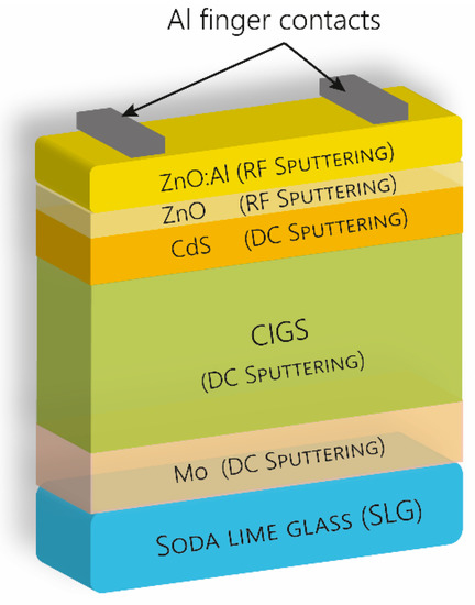
Figure 1.
The concept of copper indium gallium diselenide thin film solar cell fabricated by the use of an RF/DC magnetron sputtering system.
The bottom contact of the CIGS device is made of molybdenum (Mo) thin layer followed by heterojunction of Cu(In,Ga)Se2 p-type absorber and cadmium sulfide (CdS) buffer layer. An intrinsic zinc oxide layer is deposited on the top of CdS film. The top contact of CIGS solar cell is mostly made by transparent aluminum-doped zinc oxide (Al-ZnO) material. The total thickness of the typical CIGS solar cell structure is a few micrometers, which is much less than that of crystalline silicon ones (200–300 μm).
Complex structure of Cu(In,Ga)Se2 based solar cell requires a variety of technologies for particular layer fabrication to achieve high device efficiency. This is the reason why co-evaporation method is the most used one in the process of CIGS absorber fabrication [10,11,12] while chemical bath deposition (CBD) is a very common method of CdS buffer layer fabrication [13,14]. The application of optimal methods for each structure fabrication leads to the highest efficiency of the final device. However, at an industrial level, it can be high-priced and problematic. For this reason, an easily scalable fabrication process that consists of only one deposition system could be a promising solution for the reduction of fabrication costs [15,16].
The main purpose of the experimental work reported in this paper was to fabricate and characterize layers applied in CIGS-based solar cells (showed in Figure 1) with the use of only magnetron sputtering system. Contact films (Mo, Al, Al-ZnO), as well as Cu(In,Ga)Se2 absorber together with CdS and i-ZnO buffer, structures were investigated. Several sputtering parameters were studied to obtain contact layers with minimum value of sheet resistance. It should be emphasized that Cu(In,Ga)Se2 absorber was fabricated at relatively low substrate temperature (400 °C). The results of all structures characterization were widely discussed and compared with the results of researchers in the field. Several opened issues, as well as future plans were also pointed out.
2. Materials and Methods
Thin layers creating the CIGS device were obtained by the use of magnetron sputtering technique. In the experiments, Aliance Concept AC 450 deposition system was used, working with a static mode. The structure was prepared onto soda lime glasses (SLG) which were ultrasonically cleaned before the deposition process. The cleaning procedure provided the use of acetone and ethanol and drying in the pure nitrogen (N2) gas flow. In order to eliminate the influence of the additional parameters (e.g., shift related to the cathode center), glass substrates were located directly underneath the racetrack of the target. In the deposition process, 4-inch-diameter and 6-mm-thick ceramic targets of high purity (99.999%) were used to which the direct current (DC) or radio frequency (RF) sputtering power was applied depending on the material. To achieve the particular CIGS structures presented in Figure 1, the DC sputtering was applied to molybdenum and aluminum cathodes, while RF sputtering to quaternary Cu(In,Ga)Se, CdS, i-ZnO and ZnO:Al targets. The distance between the substrate plate and the cathode was equal to 90 mm. Each structure was created in the argon (Ar) ambient. Prior to each layer deposition process, the presputtering was carried on in order to clean the surface of targets and remove all impurities and contaminants by 15 min. Before the deposition step, the chamber was evacuated to the base pressure of 1.56 × 10⁻⁴ Pa.
In order to find the optimal properties of particular materials, experiments with various combinations of the technological parameters were conducted. A molybdenum layer was deposited in the range of sputtering power between 0.74 W/cm2 and 1.48 W/cm2 at 400 °C. The deposition times were chosen as 20, 30 and 40 min, and pressure was set as 1.53 Pa. The aluminum-doped zinc oxide layers were obtained by the use of target made of ZnO doped with 2 wt.% Al2O3 with the deposition power in the 3.08–3.95-W/cm2 range. The pressure during the deposition process was equal to 0.285 Pa. The experiments were carried out by 30 and 45 min. In order to improve ZnO:Al layers’ electrical properties, samples were additionally annealed in N2 atmosphere. The deposition of aluminum thin films occurred at room temperature with the power applied to cathode from 0.74 W/cm2 to 1.24 W/cm2 in the pressure of 1.53 Pa. An undoped ZnO target was used for i-ZnO layer deposition with sputtering power equaled to 2 W/cm2 at substrate temperature of 200 °C.
Heterojunction materials were fabricated by the use of two targets—quaternary Cu(In,Ga)Se and CdS. In both processes, the power of 1.00 W/cm2 was used. The deposition process of CIGS layers occurred within 60 min. For CdS, the deposition time was 4.5 min. The temperature of the process is vitally important, thus the substrate holder was heated up to 400 °C in the case of CIGS, and to 200 °C for CdS. The overheating of the substrate was eliminated due to the water-cooling system. The deposition pressure in both cases was equal to 1.53 Pa. The selected technological parameters of the sputtering deposition process for each thin layer are shown in Table 1.

Table 1.
Deposition parameters for each layer in CIGS-based photovoltaic structure.
The fabricated layers were examined in order to find the structural and electrical properties. The EDS profile and energy spectra were performed by the EDS detector, which is integrated with scanning electron microscope (Hitachi SU3500, Tokyo, Japan), in a vacuum condition at 20.0 kV of operating voltage. It allowed performing qualitative and quantitative analysis of the obtained layers. Surface and cross-sectional images were prepared using FEI Quanta 3D FEG scanning electron microscope (Hillsboro, OR, USA). The crystalline structure and orientation of the deposited materials were analyzed by X-ray diffraction Empyrean PANalytical Diffractometer system. Sheet resistance was determined by the use of RM3000+ four-point probe equipment of Jandel Engineering Limited at room temperature.
3. Results
3.1. Thin Contact Films for CIGS Photovoltaic Device
Figure 2 illustrates Cu Kα (λ = 1.54056 Å) XRD pattern of molybdenum (Mo) back contact film deposited on soda lime glass. As can be seen, intense (110) peak at 2θ equal to 40.5° and (211) peak at 73.5° were measured. Both locations confirm polycrystalline orientation of the molybdenum layer. The dominant peak corresponds to (110) preferred orientation for the body-centered cubic crystal structure (JCPDS Card No. 03-065-7442 [17]). Based on Scherrer equation [18] and presented diffractogram full width half maximum (FHWM) and crystalline size of Mo crystals were estimated and reported in Table 2. The calculated grain size from the highest intensity peak located at 2θ 40.5° was equal to 8 nm.
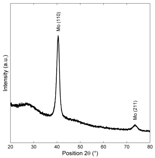
Figure 2.
XRD diffraction pattern for (110) and (211) reflection peaks of molybdenum back contact layer obtained at 1.2 W/cm2 of sputtering power and 40 min of the deposition time.
Table 2.
X-ray diffraction parameters of Mo back contact layer deposited on SLG substrate.
Figure 3 depicts Mo sheet resistance Rs dependency on sputtering power and time of the deposition process. As can be seen, sheet resistance decreases with the increase of both parameters. Our previous studies on Mo back contact [19] revealed Rs value of 4 Ω/□ for 80 W of sputtering power. Our present findings confirmed that below 80 W the sheet resistance of the film is relatively poor (Figure 3). However, for higher sputtering power sheet resistance became much lower (below 1 Ω/□) for at least 30 min of the deposition process. The best value of Rs was found to be 0.3 Ω/□ for sputtering power of 120 W and 40 min of deposition.
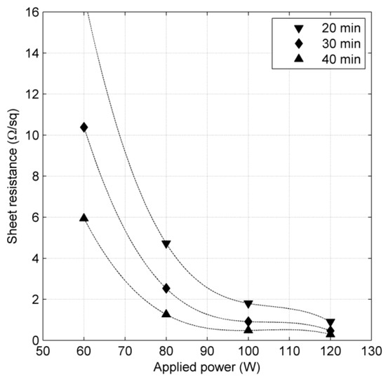
Figure 3.
Sheet resistance dependency of the molybdenum back contact films on sputtering power at different deposition times.
In order to obtain an aluminum-doped zinc oxide layer with the best sheet resistance, experimental campaign was carried out in the 250–320 W (3.08–3.95 W/cm2) power range. The deposition process was carried out in the pressure 0.287 Pa. In these studies, two deposition times were examined—30 and 45 min. Nonetheless, the layers obtained in 30 min were characterized by poor electrical conductivity. As can be seen from Figure 4, at the outset, the sheet resistance of the films, which were obtained for 250 W of power, was relatively high for implementation in the CIGS solar device. However, increasing the power to 290 W caused a decrease of the sheet resistance. The lowest Rs value, which was 141 Ω/□, occurred for a deposition time equal to 45 min. Further increasing the power applied to cathode did not cause decreasing the sheet resistance. Based on the previous studies [20], annealing treatment enhanced the electrical properties of transparent conductive oxides (TCO). Different times, up to 4 h, and temperatures in the 100–400 °C range were investigated. The best improvement of the conductivity was observed for two compilation of set parameters. In both cases, an approximately 3-fold decline was observed. The sample characterized by 141 Ω/□ was annealed in the temperature set at 300 °C by 3 h. After treatment, the Rs value decreased to 55 Ω/□.
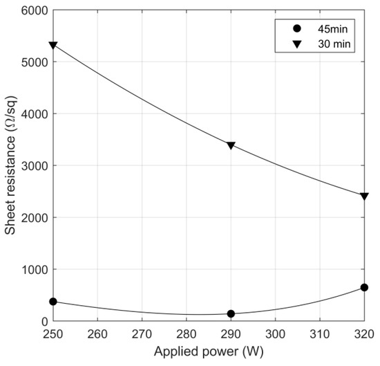
Figure 4.
Sheet resistance dependency of the ZnO:Al films on sputtering power at different deposition time.
In order to collect charges from the bottom layers, transparent conductive oxide is covered by a metal grid mostly made of few micrometers of aluminum. The most common fabrication method is evaporation; however, consequently, sputtering was used in the case of this research. Electrical properties of aluminum contact films deposited on SLG were described in previous studies [21] in detail. Figure 5 shows the dependency of aluminum films’ sheet resistance on sputtering power and deposition time. Similarly to Mo back contact, Rs decreases with the increase of sputtering power. However, in contrast to Mo back contact material, conductivity of Al layer is higher for all studied values of applied powers and times (Rs is below 0.8 Ω/□). Moreover, above 30 min of deposition, a change in Rs value with sputtering power seems to be negligible. The lowest value of Al sheet resistance was obtained for sputtering power equals 100 W and 30 min of the deposition time (0.08 Ω/□).
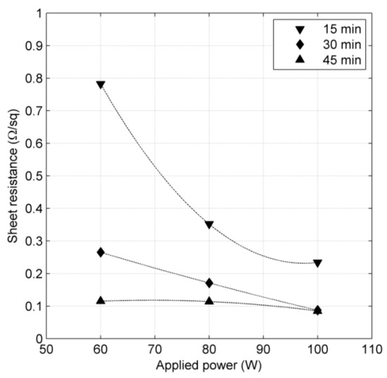
Figure 5.
Sheet resistance of aluminum top contact thin films as a function of sputtering power and deposition time.
3.2. Heterojunction Materials of CIGS Photovoltaic Device
Figure 6 shows the SEM images of copper indium gallium diselenide (CIGS) absorber deposited on Mo back contact. Smoothed surface with grains of different sizes (up to 400 nm) which is caused by relatively low temperature of the deposition process (400 °C) and high deposition pressure, can be observed.
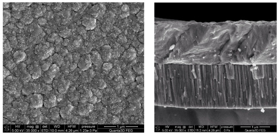
Figure 6.
SEM images of the CIGS absorber deposited on SLG substrate covered by Mo back contact film: (left) plane view and (right) cross-sectional view.
High-performance Cu(In,Ga)Se2 solar cells should be fabricated with Cu/(Ga + In) ratio (CGI) ranging from 0.7 to 1.0 and Ga/(Ga + In) ratio (GGI) between 0.2 and 0.3 [22]. In order to control both ratios, EDS analysis was carried out in this study. Figure 7 illustrates EDS spectra of CIGS absorber film deposited on soda lime glass (SLG) substrate covered by a molybdenum (Mo) back contact layer.
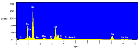
Figure 7.
EDS spectrum of the Cu(In,Ga)Se2 thin film deposited on glass substrate covered by molybdenum back contact layer.
Significant peaks of CIGS absorber elements with their characteristic X-ray energy were as follows: Cu (Kα = 8.040 keV, Lα = 0.930 keV), In (Lα = 3.286 keV), Ga (Lα = 1.098 keV) and Se (Lα = 1.379 keV). Sputtered CIGS layer was composed of about 25.9 at.% Cu, 21.6 at.% In, 5.4 at.% Ga and 45.0 at.% Se. Calculated average CGI, GGI, and Se/(Cu + In + Ga) ratios were equal to 0.96, 0.2, and 0.85 respectively. Other elements which were observed in the EDS spectra mostly came from Mo bottom layer (~2 at.%).
Figure 8 depicts Cu Kα (λ = 1.54056 Å) XRD pattern of CIGS film deposited on Mo layer. As can be seen, diffraction peaks located at 26.6°, 44.2°, 52.4°, 64.3° and 70.9° can be distinguished. They confirm formation of Cu(In,Ga)Se2 absorber (according to the JCPDS Card No. 00-035-1102 [23]). First, a very narrow and intense peak at 26.6° corresponds to (112) plane of chalcopyrite polycrystalline structure. Small width and high intensity of the presented peak proves the excellent crystalline quality of the sputtered absorber layer, which was also confirmed by the cross-sectional plane of SEM image presented in Figure 6. Another two peaks which can be easily recognized are located at 2θ position equal to 44.2° and 52.4°. They correspond to the (220)/(204) and (116)/(312) planes, respectively. These orientations allow forming better quality of p-n junction due to higher diffusivity of Cd atoms into (220)/(204)-oriented layers [24].
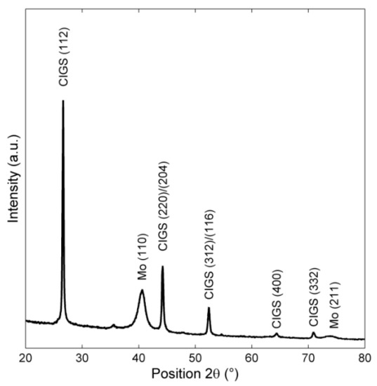
Figure 8.
XRD diffraction pattern of CIGS film deposited at a temperature of 400 °C on Mo layer.
Table 3 summarizes XRD parameters of the sputtered CIGS layer (two peaks located at 40.51° and 73.78° belong to the bottom Mo layer). The calculated grain size from the highest intensity peak located at 26.59° was 50 nm. FWHM value below 0.35 indicates high quality of deposited layer.
Table 3.
XRD parameters of CIGS absorber deposited on Mo back contact layer.
Figure 9 depicts EDS spectra of the SLG/Mo/CdS structure with characteristic peaks of CdS material: cadmium peak with characteristic X-ray energy Lα = 3.133 keV and sulfur with Kα equals 2.307 keV. CdS film was composed of 36.8 at.% of cadmium and 18.2 at.% of sulfur. Peak of molybdenum layer was also observed (with the amount of 45 at.%).
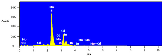
Figure 9.
EDS spectrum of the CdS buffer film deposited on CIGS absorber by magnetron sputtering technique.
In order to investigate the crystal structure and grain size of cadmium sulfide buffer, Cu Kα (λ = 1.54056 Å) XRD pattern of CdS film deposited on Mo layer was obtained (Figure 10). The temperature of the substrate during the deposition process was 200 °C.
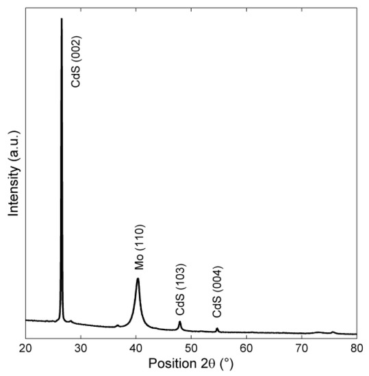
Figure 10.
XRD diffraction pattern of CdS film deposited at temperature of 200 °C on Mo layer.
Diffraction peaks located at 26.5° and 47.9° correspond to the CdS hexagonal (002) and (103) planes according to the JCPDS Card No. 01-080-0006 [25]. Similarly to the CIGS pattern presented in Figure 8, the small width and high intensity of the peaks prove the excellent crystalline quality of the formed CdS layer. In both cases (Figure 8 and Figure 10), a Mo peak located around 40° can be observed. Table 4 summarizes XRD parameters of the sputtered CdS layer. Calculated grain size from the highest intensity peak was about 191 nm.
Table 4.
XRD parameters of CdS buffer deposited on Mo substrate.
In order to fabricate heterojunction, CdS thin buffer layer was deposited onto the Cu(In,Ga)Se2 absorber film for further X-ray analysis. Figure 11 shows XRD patterns of the structures deposited on SLG substrate by magnetron sputtering method in one technological process without breaking the vacuum. Such a procedure allowed films of p-n junction in Ar neutral ambient under vacuum to be fabricated. Co Kα radiation (λ = 1.78896 Å) was used for measurements. However, position (2θ) values of XRD patterns were converted from Co Kα into Cu Kα and provided in Table 5.
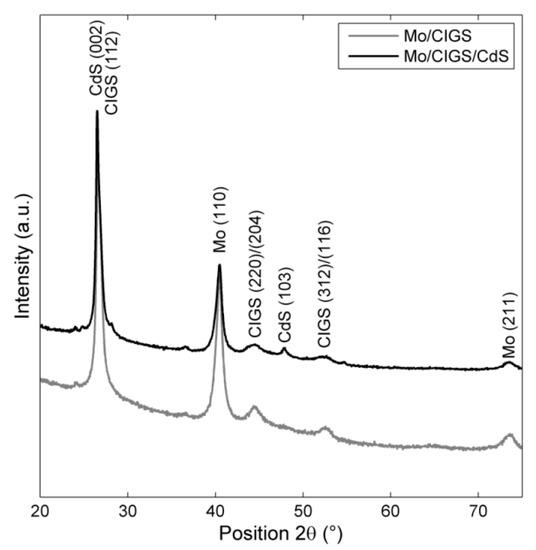
Figure 11.
Comparison of X-ray diffraction patterns of CIGS absorber deposited on SLG/Mo substrate without (below) and with (above) CdS film sputtered on the top.
Table 5.
X-ray structural parameters of CIGS/CdS layers deposited on SLG/Mo substrate.
From both diffractograms, several peaks located at the same position 2θ can be easily recognized. They correspond to molybdenum contact film (2θ = 40.4°, 2θ = 73.4°) and to the formation of Cu(In,Ga)Se2 absorber layer (2θ = 26.7°, 2θ = 44.4°, 2θ = 52.3°). Additional diffraction peaks at 26.5° and 47.8°, illustrated in Figure 11, suggest the presence of CdS crystal. Very strong, narrow peak located at 26.5° together with the peak at 47.8° confirm formation of the hexagonal oriented structure of CdS film on CIGS absorber layer. However, the grain size of CdS was 35 nm in this case which can be explained by the small grains of the CIGS bottom layer.
Moreover, Table 3, Table 4 and Table 5 show the value of inter-atomic spacing (d-spacing). For dominant peaks of Cu(In,Ga)Se2 and CdS crystals, d-spacing was found to be 0.335 and 0.336 nm, respectively. Thus, the lattice mismatch of the heterojunction between both deposited films is very small, which is desirable for good quality photovoltaic devices [22].
Figure 12 shows X-ray diffraction pattern of highly resistive i-ZnO deposited on SLG substrate at 200 °C. Similarly to the previous studies on ZnO:Al [20], a large, intense peak located at 33.93° which corresponds to the hexagonal polycrystalline structure with (002) plane was observed (according to the JCPDS Card No. 00-001-1136 [10]). The average grain size calculated from FWHM of (002) diffraction peak was about 10 nm.
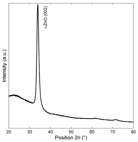
Figure 12.
XRD diffraction spectra of i-ZnO layer obtained at 200 °C on SLG substrate.
4. Discussion
The structural and electrical properties of analyzed layers deposited using only magnetron sputtering method confirmed the possibility of fabrication the highly conductive contact layers, as well as of high-quality CIGS absorber together with a CdS and i-ZnO buffer layer.
Similarly to the presented results of molybdenum (Mo) back contact film, a BCC structure with strong (110) peak at 2θ = 40.5° (Figure 2) was found by many researchers (e.g., [18,26,27]). Second, weak (211) peak at 2θ = 73.5° was also observed by Su et al. [28] for higher power applied to the cathode (between 3.5 W/cm2 and 4.5 W/cm2). Sputtering power used in these studies was in the range between 0.74 and 1.48 W/cm2. The work of [17] presents the dependency of Mo grain size on substrate temperature during the deposition process. It was shown that a higher substrate temperature leads to better crystallinity and thus to larger grains of the film. According to the result of Zhao et al. [17], the size of Mo grains varied from 11.7 nm at room temperature to 33.1 nm at 400 °C for 0.3 Pa of the sputtering pressure. The average crystallite size obtained by Su et al. [28] was around 8.7 nm at 0.67 Pa. A similar value of grain size (8 nm) was observed in the current studies for a sputtering pressure equaling 1.53 Pa. Small area devices require back contact film with sheet resistance (Rs) about 20 Ω/□ [22]. Su et al. [28] investigated the effect of sputtering power influence on sheet resistance of molybdenum film. At lower values of power applied (3.5 W/cm2), the conductivity of the Mo thin structure was poor with Rs around 4.5 Ω/□. Our results confirmed the value of 4 Ω/□ with 1 W/cm2 of power. Higher sputtering power caused decrease of Rs to 0.3 Ω/□, which can be explained by the increase of the layer thickness. The goal of the present research was to decrease the value of sheet resistance as much as possible. The obtained results are consistent with the findings of Su et al. [28] and Pethe et al. [26]. Similar to results of this paper, Rs values were presented by [29] for Al-doped zinc oxide (AZO) fabricated using an aqueous solution process followed by an UV exposure technique combined with the annealing process. The high value of Rs equals 1500 Ω/□ decreased to 36 Ω/□.
Field studies, e.g., [11,16,30], have observed similar ranges of CGI and GGI atomic ratios to that which we reported in the current study. Park et al. [16] investigated XRD patterns of CIGS thin films at substrate temperature ranging up to 600 °C. They found that all films which were grown at the temperature above 200 °C showed good crystallinity with FWHM value between 0.22° and 0.35°. The abovementioned peaks were also found by Badgujar et al. [31] where the chemical method was used to prepare a CIGS thin film. Ayachi et al. [24] observed additional (400) and (332) peaks after annealing the samples at 540 °C. Similar additional peaks were observed by Liang et al. [30] and [32] for substrate temperatures during the deposition ranging from 500 to 550 °C. Results presented in this paper reveal observation of above mentioned peaks for lower substrate temperature (400 °C) under 1.53 Pa of pressure (Table 3). From the studies of Ouyang et al. [33], the dependency of the average grain size on annealing temperature can be found. Moreover, the grain size depends not only on the temperature but also on other parameters, such as GGI ratio, sputtering pressure, and power [34]. Yu et al. [35] found the average grain size of 200 nm for the substrate temperature equaled 350 °C. Peace et al. [12] found that the grain size of the CIGS decreased with the increase of gallium content. The highest GGI (0.41) resulted in the smallest grains of size 41 nm. This value is very close to the result presented in these studies. Observations carried out by Kong et al. [23] revealed a very strong relationship between the roughness of the CIGS thin film and the working pressure.
Joshi et al. [36] published EDAX spectra of CIGS/CdS heterojunction. Significant peaks of copper (Cu), indium (In), gallium (Ga), selenium (Se) as well as cadmium (Cd) and sulphur (S) were identified. Observation of these elements is similar to our findings presented in Figure 7 and Figure 9. The XRD analysis presented in Figure 10 and Table 4 confirm preferentially oriented (002) plane located at 26.5°, which was also observed by Toma et al. [25] and Kim et al. [37]. They also used sputtering for CdS deposition. Similarly to our observations (Table 4), they measured peak (103) located at 47°. Theelen et al. [38] showed the XRD profile of the whole multilayer structure of CIGS solar cell. Similarly to our results (Figure 8), the preferred orientations of Mo (110) and CIGS (112) were detected. The same position, comparing to the result presented by Theelen et al. [38], of two another CIGS peaks ((220) and (312)) was found in these studies. Moreover, the XRD peak corresponding to the conductive oxide ZnO:Al with orientation of (002) was shown. It is consistent with the results of X-ray pattern shown in Figure 12 and our previously published research related to TCO thin film [20,39]. It should be emphasized that most of the presented XRD peaks are characterized by the low value of FWHM. Peaks related to CdS structure have an FWHM below 0.5° (Table 4) which proves high crystallinity of the CdS film. The calculated grain size of CdS was different for different substrates. It can be explained by the grain size of the layer which is under the CdS film. The d-spacing value of the highest intensity CdS peak equals 0.335 nm (Table 4) was found to be similar to the results obtained by Lee et al. [40] with the CBD method. The lattice mismatch of the obtained heterojunction is very small, which creates preferable conditions for CIGS-based device fabrication.
Several issues related to the influence of magnetron sputtering parameters on structural quality are still opened for investigation. A further experimental campaign on the improvement of CIGS absorber grain size by decrease of sputtering pressure together with the increase of sputtering power is planned. The influence of sputtering parameters on efficiency of the CIGS photovoltaic device is the most interesting goal for future research.
5. Conclusions
The magnetron sputtering technique was applied to fabricate thin film structures for CIGS solar cells application. The structural properties of the sputtered layers were analyzed using SEM, EDS and XRD methods. The sputtering parameters influence on electrical conductivity of the top and back contact materials was evaluated using four-point probe characterization. The lowest values of Rs were found to be 0.3 Ω/□ for molybdenum film and even 0.08 Ω/□ for aluminum layer. The XRD pattern of Mo film with a very intense peak confirmed body-centered cubic structure with (110) preferred orientation. The dependency of sheet resistance on sputtering power was observed in the case of transparent oxide material (Al-doped zinc oxide) used in this research. The annealing step decreased the sheet resistance of AZO layer up to three times. All fabricated contact materials were found to be suitable for CIGS fabrication in terms of electrical properties. EDS analysis confirmed correct stoichiometry of the CIGS absorber. Calculated CGI and GGI ratios were found to be 0.96 and 0.2, respectively. X-ray diffractograms revealed very narrow and intense diffraction peaks typical for polycrystalline chalcopyrite CIGS crystal. FWHM value below 0.35 confirmed the possibility of high-quality absorber fabrication at a relatively low substrate temperature of 400 °C under 1.53 Pa of deposition pressure. XRD studies on CdS and i-ZnO layers confirmed the presence of the hexagonal structures. Finally, a small lattice mismatch of the p-n heterojunction materials was detected.
Author Contributions
Conceptualization, S.G.; methodology, S.G. and E.K.; software, E.K.; formal analysis, S.G.; investigation, S.G. and E.K.; writing S.G. and E.K.; visualization, E.K.; supervision, S.G.; All authors have read and agreed to the published version of the manuscript.
Funding
This work was supported by Polish Ministry of Science and Higher Education.
Conflicts of Interest
The authors declare no conflict of interest.
References
- Fraunhofer ISE. Available online: https://www.ise.fraunhofer.de/de.html (accessed on 18 March 2020).
- Hernández-Callejo, L.; Gallardo-Saavedra, S.; Alonso-Gómez, V. A review of photovoltaic systems: Design, operation and maintenance. Sol. Energy 2019, 188, 426–440. [Google Scholar] [CrossRef]
- Wang, Y.-C.; Wu, T.-T.; Chueh, Y.-L. A critical review on flexible Cu(In, Ga)Se2 (CIGS) solar cells. Mater. Chem. Phys. 2019, 234, 329–344. [Google Scholar] [CrossRef]
- Lee, T.D.; Ebong, A.U. A review of thin film solar cell technologies and challenges. Renew. Sustain. Energy Rev. 2017, 70, 1286–1297. [Google Scholar] [CrossRef]
- Gulkowski, S.; Zdyb, A.; Dragan, P. Experimental Efficiency Analysis of a Photovoltaic System with Different Module Technologies under Temperate Climate Conditions. Appl. Sci. 2019, 9, 141. [Google Scholar] [CrossRef]
- Zdyb, A.; Gulkowski, S. Performance Assessment of Four Different Photovoltaic Technologies in Poland. Energies 2020, 13, 196. [Google Scholar] [CrossRef]
- Solar Cell Efficiency Tables (Version 53) Green 2019 Progress in Photovoltaics: Research and Applications Wiley Online Library. Available online: https://onlinelibrary.wiley.com/doi/10.1002/pip.3102 (accessed on 18 March 2020).
- Dhere, N.G. Scale-up issues of CIGS thin film PV modules. Sol. Energy Mater. Sol. Cells 2011, 95, 277–280. [Google Scholar] [CrossRef]
- Ramanujam, J.; Bishop, D.M.; Todorov, T.K.; Gunawan, O.; Rath, J.; Nekovei, R.; Artegiani, E.; Romeo, A. Flexible CIGS, CdTe and a-Si:H based thin film solar cells: A review. Prog. Mater. Sci. 2020, 110, 100619. [Google Scholar] [CrossRef]
- Alhammadi, S.; Park, H.; Kim, W.K. Optimization of Intrinsic ZnO Thickness in Cu(In,Ga)Se2-Based Thin Film Solar Cells. Materials 2019, 12, 1365. [Google Scholar] [CrossRef]
- Huang, C.-H.; Chuang, W.-J.; Lin, C.-P.; Jan, Y.-L.; Shih, Y.-C. Deposition Technologies of High-Efficiency CIGS Solar Cells: Development of Two-Step and Co-Evaporation Processes. Crystals 2018, 8, 296. [Google Scholar] [CrossRef]
- Peace, B.; Claypoole, J.; Sun, N.; Dwyer, D.; Eisaman, M.D.; Haldar, P.; Efstathiadis, H. Characterization of Cu(In,Ga)Se2 (CIGS) films with varying gallium ratios. J. Alloys Compd. 2016, 657, 873–877. [Google Scholar] [CrossRef]
- Alhammadi, S.; Moon, K.; Park, H.; Kim, W.K. Effect of different cadmium salts on the properties of chemical-bath-deposited CdS thin films and Cu(InGa)Se2 solar cells. Thin Solid Film 2017, 625, 56–61. [Google Scholar] [CrossRef]
- Salomé, P.M.P.; Keller, J.; Törndahl, T.; Teixeira, J.P.; Nicoara, N.; Andrade, R.-R.; Stroppa, D.G.; González, J.C.; Edoff, M.; Leitão, J.P.; et al. CdS and Zn1−xSnxOy buffer layers for CIGS solar cells. Sol. Energy Mater. Sol. Cells 2017, 159, 272–281. [Google Scholar] [CrossRef]
- Rosa, G.; Bosio, A.; Menossi, D.; Romeo, N. How the Starting Precursor Influences the Properties of Polycrystalline CuInGaSe2 Thin Films Prepared by Sputtering and Selenization. Energies 2016, 9, 354. [Google Scholar] [CrossRef]
- Park, J.C.; Al-Jassim, M.; Shin, S.W.; Kim, J.H.; Kim, T.W. Comprehensive characterization of CIGS absorber layers grown by one-step sputtering process. Ceram. Int. 2019, 45, 4424–4430. [Google Scholar] [CrossRef]
- Zhao, H.; Xie, J.; Mao, A.; Wang, A.; Chen, Y.; Liang, T.; Ma, D. Effects of Heating Mode and Temperature on the Microstructures, Electrical and Optical Properties of Molybdenum Thin Films. Materials 2018, 11, 1634. [Google Scholar] [CrossRef] [PubMed]
- Rashid, H.; Rahman, K.S.; Hossain, M.I.; Nasser, A.A.; Alharbi, F.H.; Akhtaruzzaman, M.; Amin, N. Physical and electrical properties of molybdenum thin films grown by DC magnetron sputtering for photovoltaic application. Res. Phys. 2019, 14, 102515. [Google Scholar] [CrossRef]
- Gułkowski, S.; Krawczak, E. Experimental studies of thin films deposition by magnetron sputtering method for CIGS solar cell fabrication. E3S Web Conf. 2017, 19, 03006. [Google Scholar] [CrossRef]
- Zdyb, A.; Krawczak, E.; Gułkowski, S. The influence of annealing on the properties of ZnO:Al layers obtained by RF magnetron sputtering. Opto-Electron. Rev. 2018, 26, 247–251. [Google Scholar] [CrossRef]
- Krawczak, E.; Gułkowski, S. Electrical properties of aluminum contacts deposited by DC sputtering method for photovoltaic applications. E3S Web Conf. 2017, 19, 03011. [Google Scholar] [CrossRef]
- Luque, A.; Hegedus, S. (Eds.) Handbook of Photovoltaic Science and Engineering; John Wiley & Sons: Chichester, UK, 2003; ISBN 0-471-49196-9. [Google Scholar]
- Kong, H.; He, J.; Huang, L.; Zhu, L.; Sun, L.; Yang, P.; Chu, J. Effect of working pressure on growth of Cu(In,Ga)Se2 thin film deposited by sputtering from a single quaternary target. Mater. Lett. 2014, 116, 75–78. [Google Scholar] [CrossRef]
- Ayachi, B.; Aviles, T.; Vilcot, J.-P.; Sion, C.; Miska, P. Room temperature pulsed-DC sputtering deposition process for CIGS absorber layer: Material and device characterizations. Thin Solid Films 2018, 660, 175–179. [Google Scholar] [CrossRef]
- Toma, O.; Ion, L.; Iftimie, S.; Radu, A.; Antohe, S. Structural, morphological and optical properties of rf—Sputtered CdS thin films. Mater. Des. 2016, 100, 198–203. [Google Scholar] [CrossRef]
- Pethe, S.A.; Takahashi, E.; Kaul, A.; Dhere, N.G. Effect of sputtering process parameters on film properties of molybdenum back contact. Sol. Energy Mater. Sol. Cells 2012, 100, 1–5. [Google Scholar] [CrossRef]
- Chelvanathan, P.; Shahahmadi, S.A.; Arith, F.; Sobayel, K.; Aktharuzzaman, M.; Sopian, K.; Alharbi, F.H.; Tabet, N.; Amin, N. Effects of RF magnetron sputtering deposition process parameters on the properties of molybdenum thin films. Thin Solid Films 2017, 638, 213–219. [Google Scholar] [CrossRef]
- Su, C.-Y.; Liao, K.-H.; Pan, C.-T.; Peng, P.-W. The effect of deposition parameters and post treatment on the electrical properties of Mo thin films. Thin Solid Films 2012, 520, 5936–5939. [Google Scholar] [CrossRef]
- Liu, R.; Chen, Y.; Ding, S.; Li, Y.; Tian, Y. Preparation of highly transparent conductive aluminum-doped zinc oxide thin films using a low-temperature aqueous solution process for thin-film solar cells applications. Sol. Energy Mater. Sol. Cells 2019, 203, 110161. [Google Scholar] [CrossRef]
- Liang, G.-X.; Fan, P.; Chen, C.-M.; Zheng, Z.-H.; Zhang, D.-P. A promising sputtering for in situ fabrication of CIGS thin films without post-selenization. J. Alloys Compd. 2014, 610, 337–340. [Google Scholar] [CrossRef]
- Badgujar, A.C.; Dusane, R.O.; Dhage, S.R. Cu(In,Ga)Se2 thin film absorber layer by flash light post-treatment. Vacuum 2018, 153, 191–194. [Google Scholar] [CrossRef]
- Chen, C.-H.; Lin, T.-Y.; Hsu, C.-H.; Wei, S.-Y.; Lai, C.-H. Comprehensive characterization of Cu-rich Cu(In,Ga)Se2 absorbers prepared by one-step sputtering process. Thin Solid Films 2013, 535, 122–126. [Google Scholar] [CrossRef]
- Ouyang, L.; Zhao, M.; Zhuang, D.; Han, J.; Gao, Z.; Guo, L.; Li, X.; Sun, R.; Cao, M. Annealing treatment of Cu(In,Ga)Se2 absorbers prepared by sputtering a quaternary target for 13.5% conversion efficiency device. Sol. Energy 2015, 118, 375–383. [Google Scholar] [CrossRef]
- Frantz, J.A.; Bekele, R.Y.; Nguyen, V.Q.; Sanghera, J.S.; Bruce, A.; Frolov, S.V.; Cyrus, M.; Aggarwal, I.D. Cu(In,Ga)Se2 thin films and devices sputtered from a single target without additional selenization. Thin Solid Films 2011, 519, 7763–7765. [Google Scholar] [CrossRef]
- Yu, Z.; Yan, Y.; Li, S.; Zhang, Y.; Yan, C.; Liu, L.; Zhang, Y.; Zhao, Y. Significant effect of substrate temperature on the phase structure, optical and electrical properties of RF sputtered CIGS films. Appl. Surf. Sci. 2013, 264, 197–201. [Google Scholar] [CrossRef]
- Joshi, R.A.; Gupta, M.; Phase, D.M. Annealing induced modifications in physicochemical and optoelectronic properties of CdS/CuInGaSe2 thin film. Sol. Energy 2019, 177, 1–7. [Google Scholar] [CrossRef]
- Kim, D.; Park, Y.; Kim, M.; Choi, Y.; Park, Y.S.; Lee, J. Optical and structural properties of sputtered CdS films for thin film solar cell applications. Mater. Res. Bull. 2015, 69, 78–83. [Google Scholar] [CrossRef]
- Theelen, M.; Hendrikx, R.; Barreau, N.; Steijvers, H.; Böttger, A. The effect of damp heat-illumination exposure on CIGS solar cells: A combined XRD and electrical characterization study. Sol. Energy Mater. Sol. Cells 2016, 157, 943–952. [Google Scholar] [CrossRef]
- Krawczak, E.; Zdyb, A.; Gulkowski, S.; Fave, A.; Fourmond, E. Influence of sputtering deposition parameters on electrical and optical properties of aluminium-doped zinc oxide thin films for photovoltaic applications. E3S Web Conf. 2017, 22, 00090. [Google Scholar] [CrossRef]
- Lee, S.; Lee, E.S.; Kim, T.Y.; Cho, J.S.; Eo, Y.J.; Yun, J.H.; Cho, A. Effect of annealing treatment on CdS/CIGS thin film solar cells depending on different CdS deposition temperatures. Sol. Energy Mater. Sol. Cells 2015, 141, 299–308. [Google Scholar] [CrossRef]


© 2020 by the authors. Licensee MDPI, Basel, Switzerland. This article is an open access article distributed under the terms and conditions of the Creative Commons Attribution (CC BY) license (http://creativecommons.org/licenses/by/4.0/).