Article

Highly Transparent Conducting Electrodes Based on a Grid Structure of Silver Nanowires

School of Chemical Engineering and Materials Science, Chung-Ang University, 84 Heukseok-ro, Dongjak-gu, Seoul 06974, Korea
*
Author to whom correspondence should be addressed.
Coatings 2021, 11(1), 30; https://doi.org/10.3390/coatings11010030
Submission received: 9 December 2020 / Revised: 25 December 2020 / Accepted: 28 December 2020 / Published: 30 December 2020

Abstract

:
Transparent conducting electrodes (TCEs) formed with silver nanowires (AgNWs) have attracted attention as substitutes for indium tin oxide (ITO). However, the randomly deposited AgNW film performs poorly in terms of the transmittance and sheet resistance to serve as a substitute of ITO. To improve the performance of the AgNW film, we fabricated a grid-patterned AgNW by modifying the surface energy of the substrate. The hydrophobized surface was selectively etched by UV light through a quartz chrome mask, and a suspension of AgNWs in isopropyl alcohol/ethylene glycol mixture was coated on the substrate by a meniscus dragging deposition process. The grid-patterned AgNW film has a lower percolation threshold and a 13% higher figure-of-merit value compared to the randomly deposited AgNW film. The transparent thin films with a grid structure of AgNWs exhibit the high electrical conductivity with a sheet resistance of 33 Ohm/sq at a transmittance of 92.7% (λ = 550 nm).

1. Introduction

Transparent conducting electrodes (TCEs) have been actively researched for use in electronic devices, such as transparent heaters, displays, touch screens, solar cells, and wearable devices [1,2]. Indium tin oxide (ITO) is the most commonly used material for transparent electrodes. However, the scarcity of indium, the need for high vacuum in the processing of ITO, and the rigidity of ITO are the drawbacks of using the ITO electrode. Although efforts have been made to overcome these flaws, the improvements made are inadequate to satisfy the demand of future electronics [3]. Thus, numerous studies are devoted to replace ITO with other conductive materials. Potential candidates include metal oxides [4,5], carbon nanotubes [6,7], graphene [2,8], metal nanoparticle [9], and metal nanowires [10,11]. Among these materials, silver nanowire (AgNW) is being spotlighted, owing to its high conductivity and flexibility [12]. In addition, a suspension of AgNWs can be easily mass-produced by the polyol method [13,14,15].
Many researchers have fabricated transparent electrodes with AgNWs by different coating methods. Numerous methods, such as spin-coating [16], spray-coating [17], vacuum filtration [18], and Langmuir-Blodgett assembly [19], are used for depositing nanomaterials on a substrate. Most of the structures of AgNWs deposited by these methods have a random network structure. However, the transmittance and sheet resistance of the randomly deposited AgNW films are not adequate to replace ITO. To overcome this issue, researchers have tried to control the radius and length of metal nanowires [20], their orientation [11], or have mixed the metal nanowires with other conductive materials [21,22,23,24]. In addition, there have been efforts to fabricate patterned AgNW films by polymer-assisted metal nanowire printing [25], spin-coating on selectively oxidized surface of a polydimethylsiloxane (PDMS) substrate [26], dry-film photoresist process [27], and selective control of adhesion between AgNWs and substrates [28].
In this study, a new approach for fabricating AgNW grid-patterned electrodes is realized based on dewetting-driven micropatterning, driven by surface energy gradient [29]. Precise control of dewetting phenomena was achieved by combination of optimizing rheological properties of AgNW dispersion by adding ethylene glycol (EG) and forming uniform liquid thin film on the octadecyltrichlorosilane (OTS) grid-patterned substrate. Meniscus dragging deposition (MDD), previously reported by our group [8] is used to produce uniform liquid thin film on OTS pre-patterned substrate and UV-ozone etching is used to pattern OTS layer, generating a large surface gradient between hydrophobic OTS area and hydrophilic etched area. Based on this strategy, wide-ranged control of transmittance and sheet resistance was easily achieved by adjusting coating parameters, including EG concentration, pattern design, and deposition velocity. Especially, reliable control of sheet resistance and transmittance in high transmittance region was easily achieved by lowering percolation threshold of AgNW networked film. In addition to this, our grid-structure AgNW electrodes also exhibit outstanding optical transmittance and conductivity compared to recently reported AgNW based electrodes, confirming validity of our dewetting-driven micropatterning process.

2. Materials and Methods

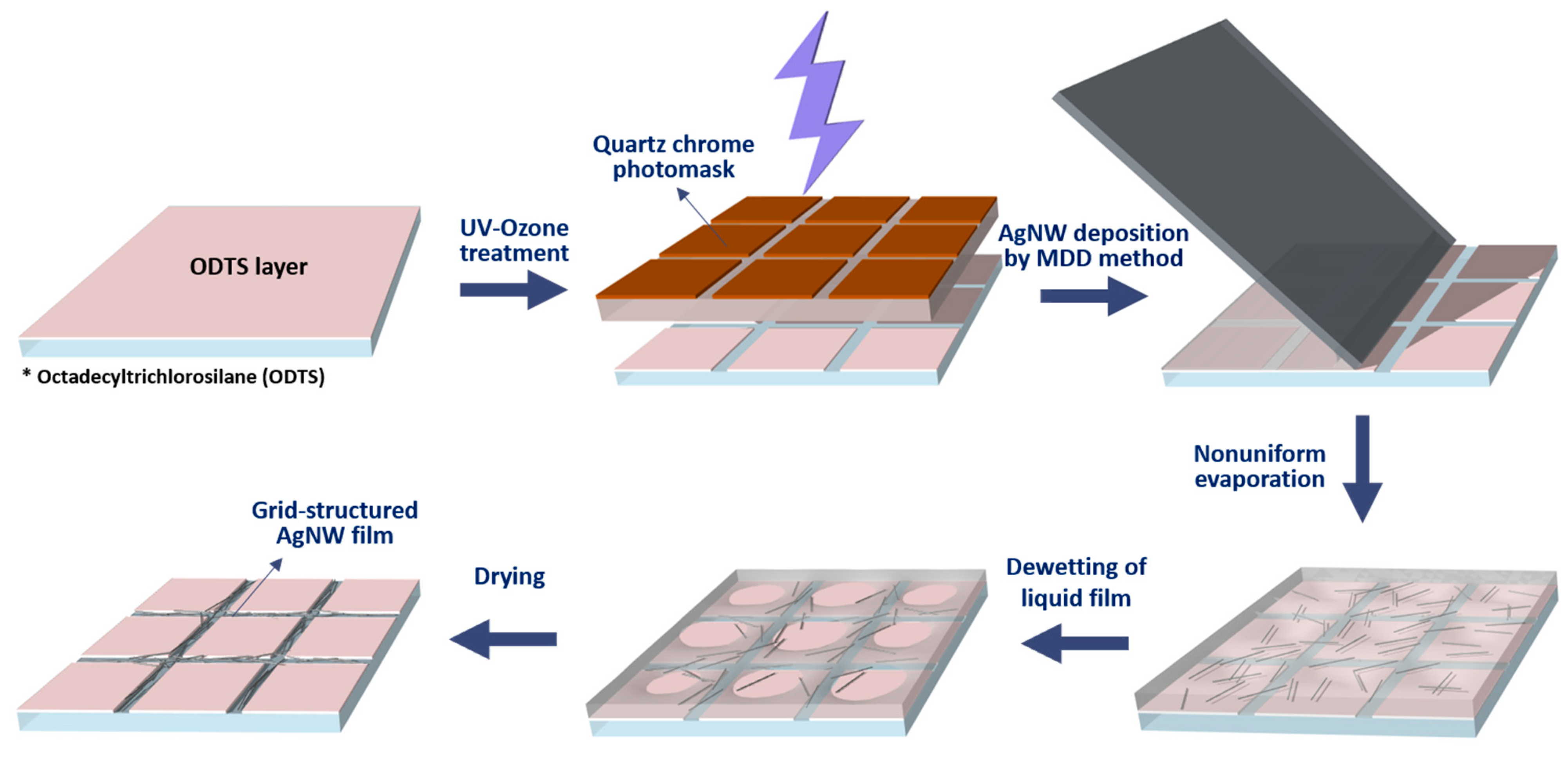
2.1. Preparation of Substrates

Glass substrates (25 × 75 mm2, Fisher Scientific, Hampton, NH, USA) were cleaned by immersion in a Piranha solution at 180 °C for 6 h. They were then rinsed several times with deionized (DI) water (Human Power II+, Human Corporation, Seoul, Korea) and dried with nitrogen gas blowing. For further hydrophilization, the substrates were treated with air plasma (PDC-32G, Harrick Plasma, manufacturer, Ithaca, NY, USA) for 15 min. Meanwhile, OTS (Sigma-Aldrich, St. Louis, MO, USA) was mixed with anhydrous toluene (99.8%, Alfa Aesar, Haverhill, MA, USA) in a glove box to prepare a 0.3 vol.% OTS solution. OTS was stored in a glove box filled with nitrogen to prevent the polymerization of OTS by reaction with moisture in air. Thereafter, the substrates were immersed in the OTS solution for 1 h. Subsequently, the glass substrates were rinsed with toluene (Daejung, Siheung, Korea) and dried with nitrogen gas blowing. The substrates were then cut into three pieces (25 × 25 mm2) and sonicated (CPX5800H-E, Emerson, St. Louis, MO, USA) with toluene for 2 h. OTS SAM-treated substrates were sequentially rinsed with toluene, ethanol, and DI water. They were then blown dried with nitrogen gas. The contact angles of the substrates were determined by measuring and averaging the contact angles at three points on the surface, using a contact angle measuring machine (Smart Drop, Femtofab, Seongnam, Korea).

2.2. Patterning of the Substrates

An OTS SAM-treated substrate was fixed between a grid-patterned quartz chrome mask and fabric-wrapped mask using a custom-made device. It was then exposed to UV light through the quartz chrome mask for 1 h to etch the OTS layer and form a grid pattern. Air was circulated with a pump to prevent the unnecessary oxidation of the substrate during its exposure.

2.3. Fabrication of AgNW Films

A 0.5 wt.% suspension of AgNWs (average diameter: 40 nm, average length: 20 μm, and dispersed in IPA) was purchased from DS Hi-metal, South Korea. The coating mixture was prepared by adding EG (Sigma-Aldrich, St. Louis, MO, USA) to 2 vol.% of the AgNW suspension. The AgNW thin films were coated on the OTS-patterned substrate by the MDD method. A piranha-treated deposition plate (76 × 52 mm2, MATSUNAMI, Osaka, Japan) was set on the coating substrate at an angle of 30°. Subsequently, 20 μL of the coating mixture was injected between the deposition plate and substrate. The deposition plate was moved forward and backward three consecutive times using a motion controller (AL1-1515-3S, Micro Motion Technology, Incheon, Korea) at a steady speed of 4 cm/s. One cycle of forward and backward movement is defined as one deposition (deposition number (DN) = 1). A DN of 3 was commonly used for the deposition of AgNWs. After the liquid film was fully dried, the substrate was annealed at 200 °C for 1 h in ambient air.

2.4. Characterization of AgNW Films

Optical images of AgNW films were obtained by digital photography (Lumix DMC-LX5, Panasonic, Osaka, Japan) and field-emission scanning electron microscopy (Carl Zeiss, Oberkochen, Germany) images were obtained by a Carl Zeiss Sigma system. The absorbance of the AgNW dispersion and the transmittance spectra of the AgNW films were recorded by an UV-vis spectrophotometer (V-670, JASCO, Easton, MD, USA). The measurements were performed at three locations on the films. The sheet resistance (RSh) of the films was measured using a four-point probe station (M3P302-system, MSTECH, Anyang, Korea) with a Keithley 2612A source meter.

3. Results and Discussion

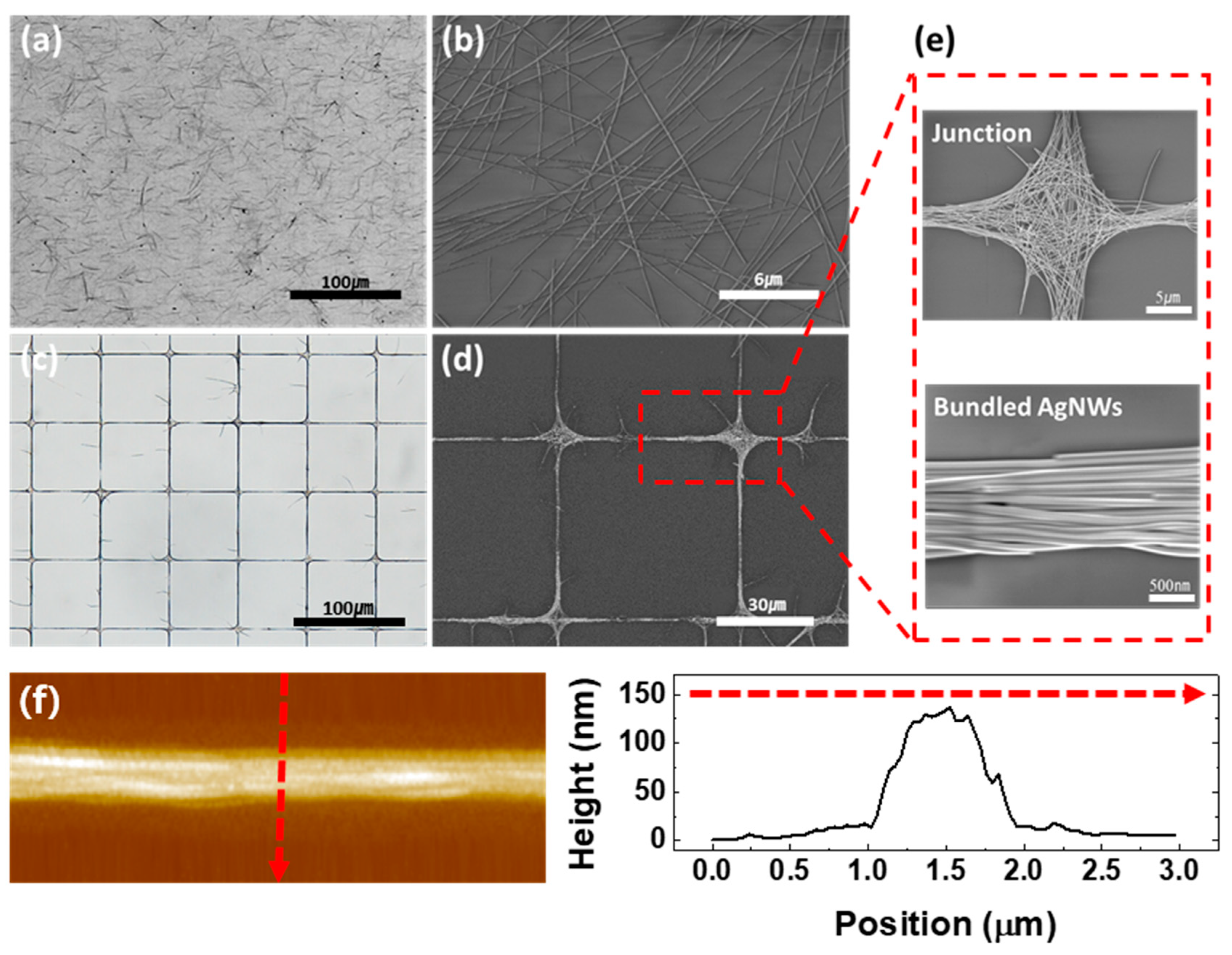
3.1. Fabrication of TCEs Based on Grid-Patterned AgNWs

The fabrication procedure for the grid-structured AgNW films is illustrated in Figure 1. The glass substrates were cleaned and hydrophilized by piranha treatment and air plasma treatment to facilitate the formation of OTS SAMs on the glass substrates. Hydrophobic glass substrates with a water contact angle of approximately 100°–110° were obtained after immersion in the OTS solution for 1 h. The OTS SAM was selectively etched by exposing the substrate to UV light through a grid-patterned quartz chrome mask, generating a grid-patterned hydrophilic region [30,31]. A uniform liquid thin film, containing AgNWs was formed on the OTS pre-patterned substrate via MDD, resulting in spontaneous dewetting of liquid thin film. Then, a grid-structured AgNW electrode was obtained after solvent drying.

3.2. Principle of Pattern Formation

AgNWs were dragged to the hydrophilized area via the dewetting of the liquid thin film of the coating mixture on the substrate. The solvents used in the coating mixture are IPA and EG, which have a large difference in surface tension (IPA: 21.4 mN/m, EG: 48.4 mN/m) [32]. Therefore, IPA vaporized at a higher rate than EG, which resulted in a gradual increase in the concentration of EG after the deposition of the mixture on the substrate. The higher EG concentration leads to the increment of the surface tension of the liquid thin film on the substrate. Therefore, the liquid film is dewetted from the hydrophobic OTS SAM area and moves to the plasma-etched area with a high surface energy from hydroxyl groups. Simultaneously, the AgNWs are transferred to the plasma-etched area by the dewetting-driven liquid flux, resulting in the formation of the grid-structured AgNW film.

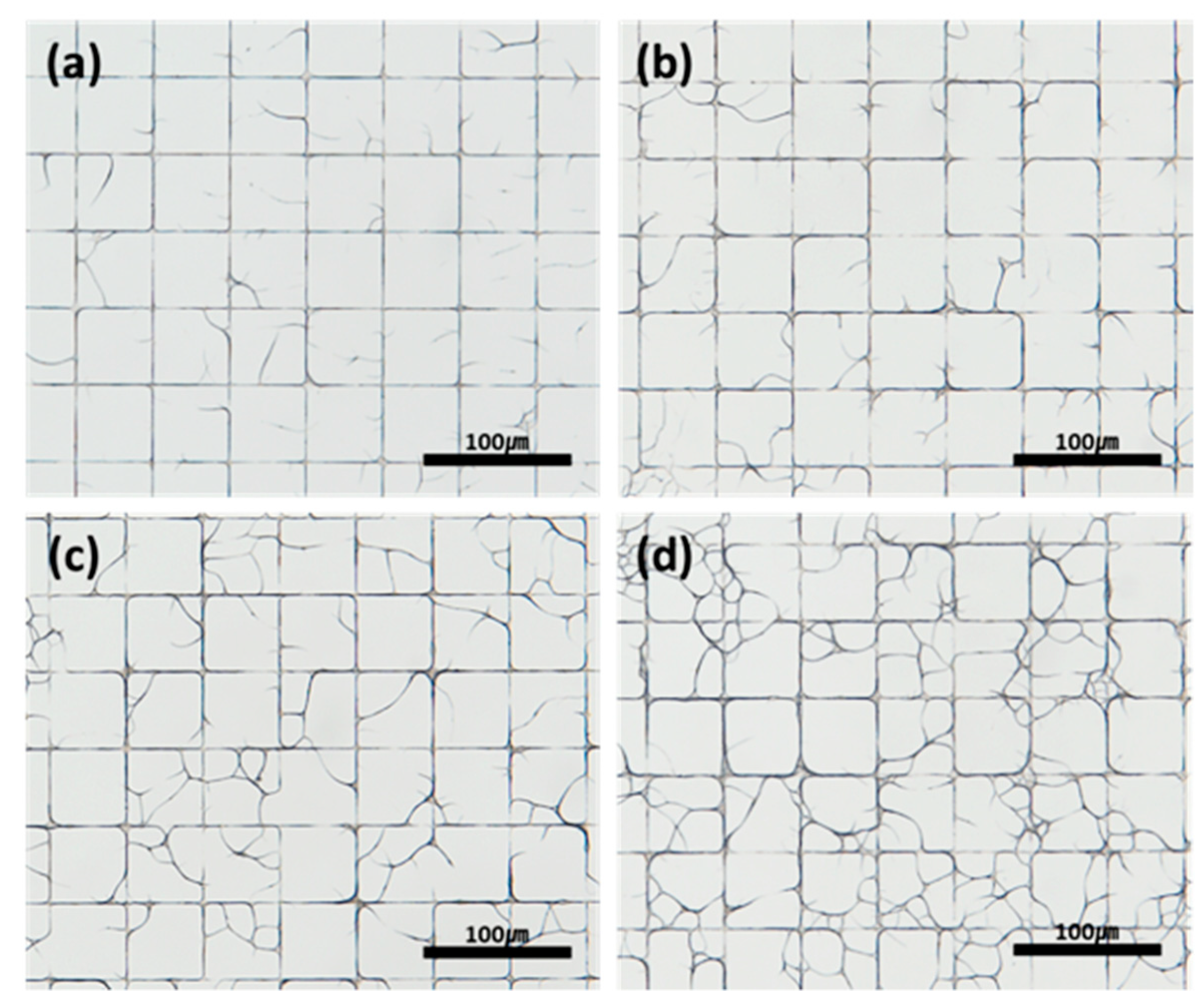
3.3. Effect of Pattern Design

Figure 2 shows the optical images of the patterned AgNW films with various grid widths (1, 2, 5, and 10 μm) at a fixed spacing of 40 μm. When the width of the grid was 1 μm, the AgNWs tended to agglomerate at the junction of the grid (Figure 2a). In contrast, as shown in Figure 2c,d, when the width of grid was 5 and 10 μm, the AgNWs are scattered in the grid because the liquid was pinned at the border of the grid and it spread in the hydrophilic area [33] and the amount of AgNW also is not enough to fill the grid area. However, when the width was 2 μm (Figure 2b), the well-defined grid-structure of AgNW film was obtained (Figure 2b). Therefore, the following experiments were conducted with a fixed width of 2 μm.

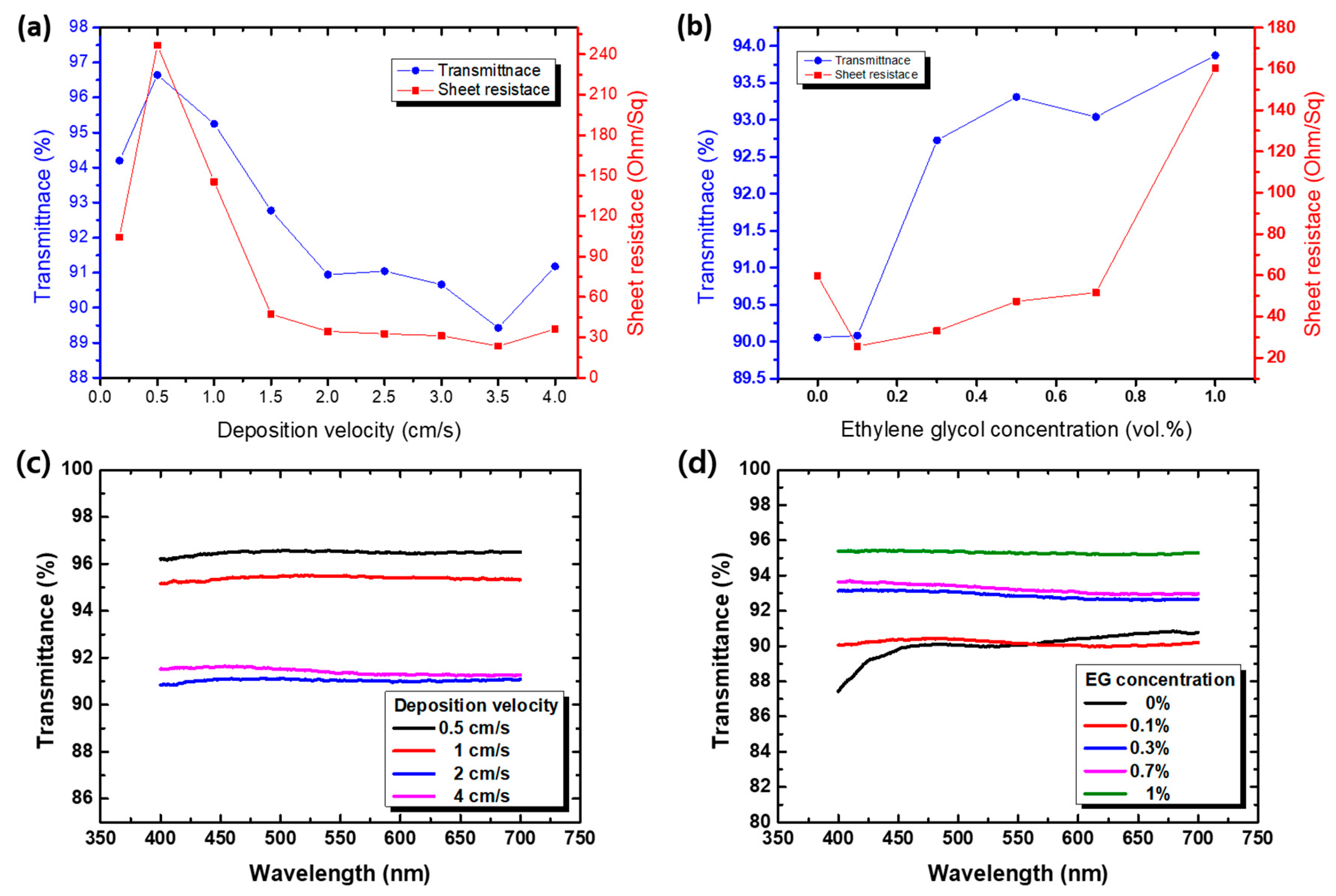
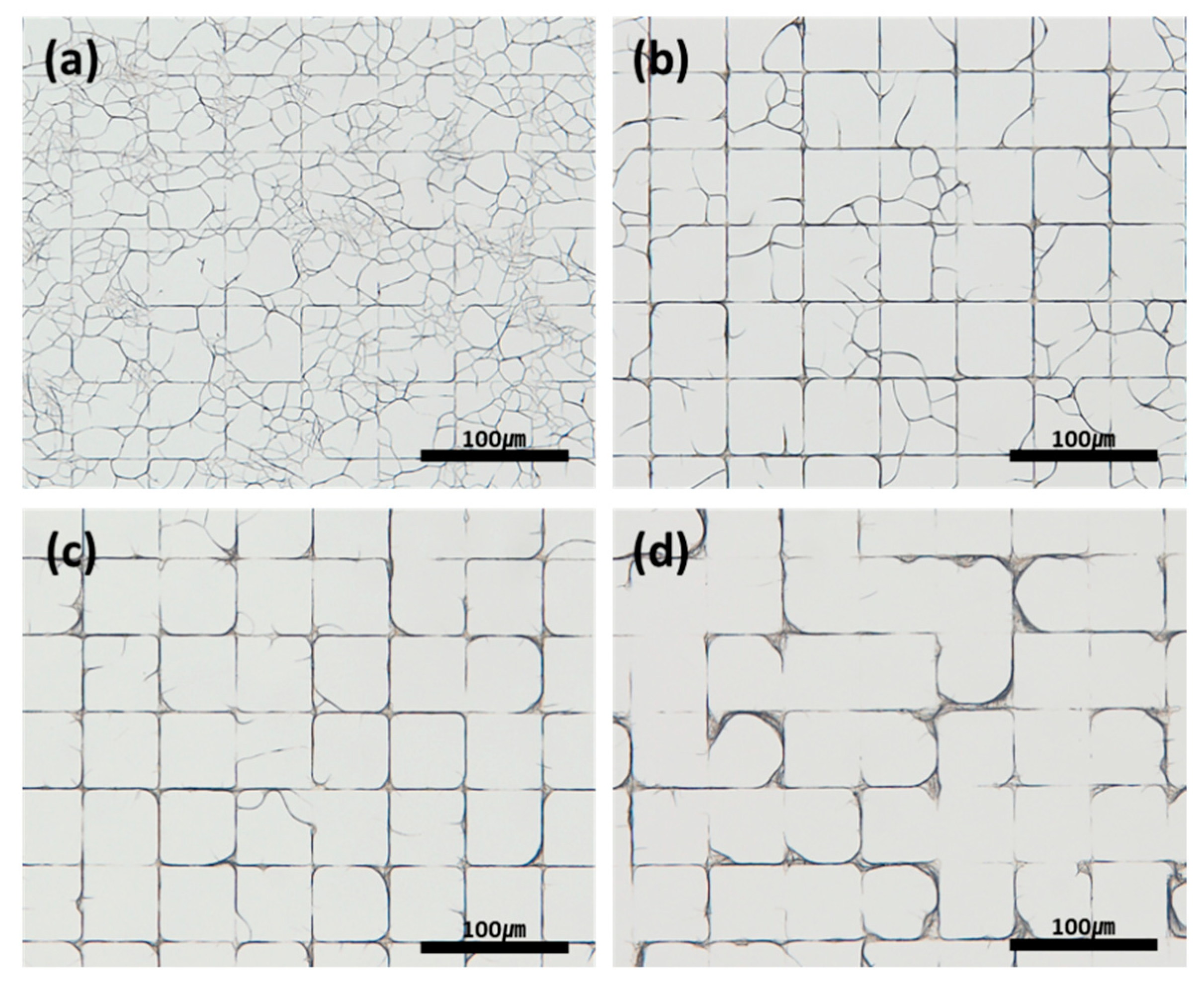
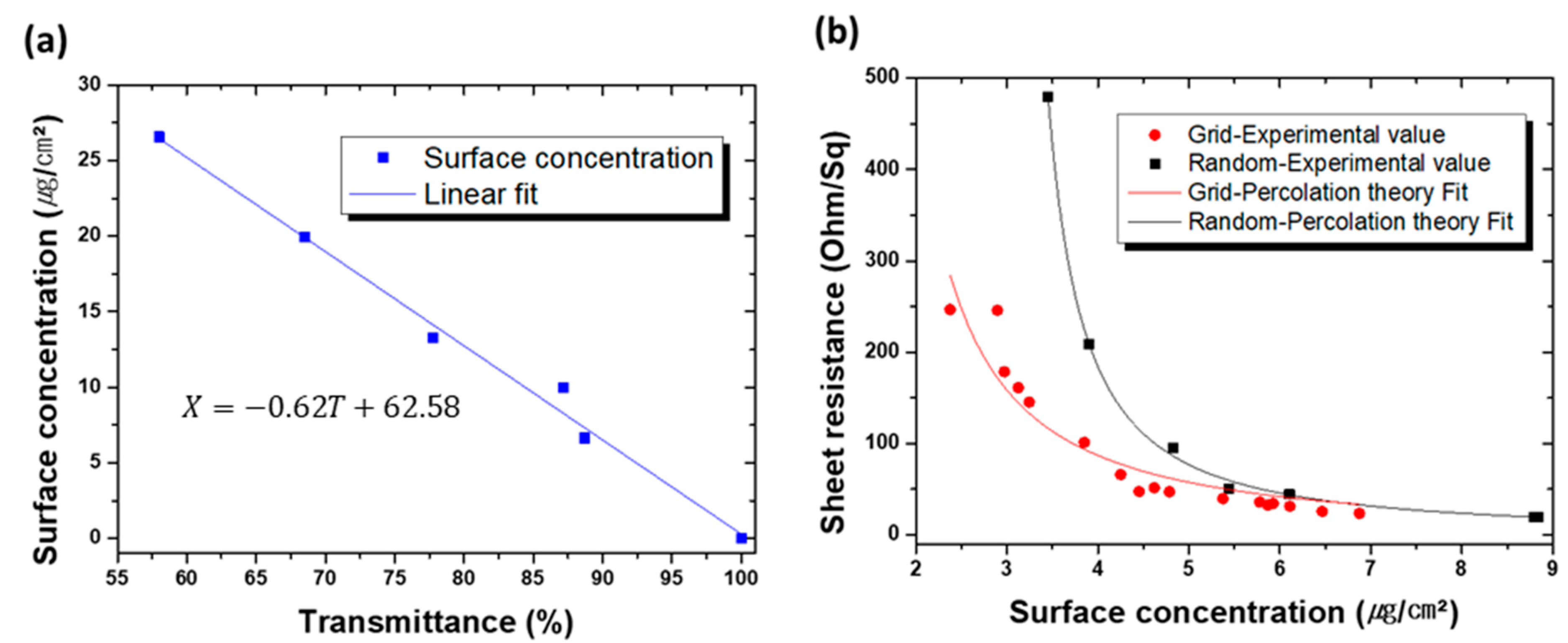
3.4. Effect of the Deposition Conditions

The thickness of the liquid thin film obtained by the MDD process can be defined by the Landau–Levich–Derjaquin (LLD) model, which is expressed in the form of Equation (1) [34].
h l i q = 1.34 ( μ V γ ) 2 3 R
where μ is the viscosity of the coating liquid, V is the deposition velocity (DV), γ is the surface tension of the liquid, and R is the radius of the meniscus. The radius of the meniscus, R, can be controlled by adjusting the injection volume of the coating mixture. V and R can be changed to control the thickness of the liquid film without a change in the liquid composition. Therefore, in this study, only the deposition velocity was changed because increasing the injection volume of the coating mixture also increases the waste of AgNWs.
Equation (1) explains how the properties of the electrodes change with the DV. According to the equation, a higher DV increases the film thickness. Therefore, the solvent evaporation time was lengthened. Further, a longer evaporation time maximized the effect of the Marangoni flow. The Marangoni flow occurs in the film of a liquid mixture because of non-uniform solvent evaporation, causing the deposition of AgNWs on the substrate [35]. Therefore, numerous AgNWs were already deposited and anchored on the substrate during the dewetting of the liquid film. Hence, AgNWs tended to form a hybrid structure of web networks in the square area of the grid pattern (Figure 3). The grid-structured AgNW electrodes on the glass substrate were annealed at 200 °C for 60 min in order to enhance the electrical conductivity by removing the PVP layer and EG residue. The transmittance and sheet resistance also changed with the variation in DV (Figure 4). The transmittance decreased as the DV increased, whereas the sheet resistance increased, owing to the web network of AgNWs in the square area of the grid. At the lowest DV (0.17 cm/s) that could be programmed by the motion controller, a very thin liquid film formed and rapidly reached the critical thickness. Therefore, the liquid film was not maintained and it contracted during the coating process. Therefore, few AgNWs were deposited on the substrate, resulting in different tendencies in transmittance and sheet resistance.
The structure of AgNW networks can be changed by controlling the concentration of EG (Figure 5). At a low EG concentration (Figure 5), there were more web networks of AgNWs than grid networks because the dewetting force was very weak to pull all the AgNWs to the hydrophilic area. At the optimal concentration (Figure 5), the grid structure was mainly formed because of the increased dewetting force. However, the AgNWs began to concentrate at the junction of the grid and lose contact with the side of the grid when the EG concentration was too high (Figure 5). The optoelectrical properties also changed upon varying the EG concentration (Figure 4). The transmittance increased as the concentration increased, owing to the convergence of the AgNWs toward the etched area, whereas the sheet resistance decreased because of the disconnections at the side. In addition, the web networks diminished, causing an increase in transmittance and a decrease in sheet resistance.

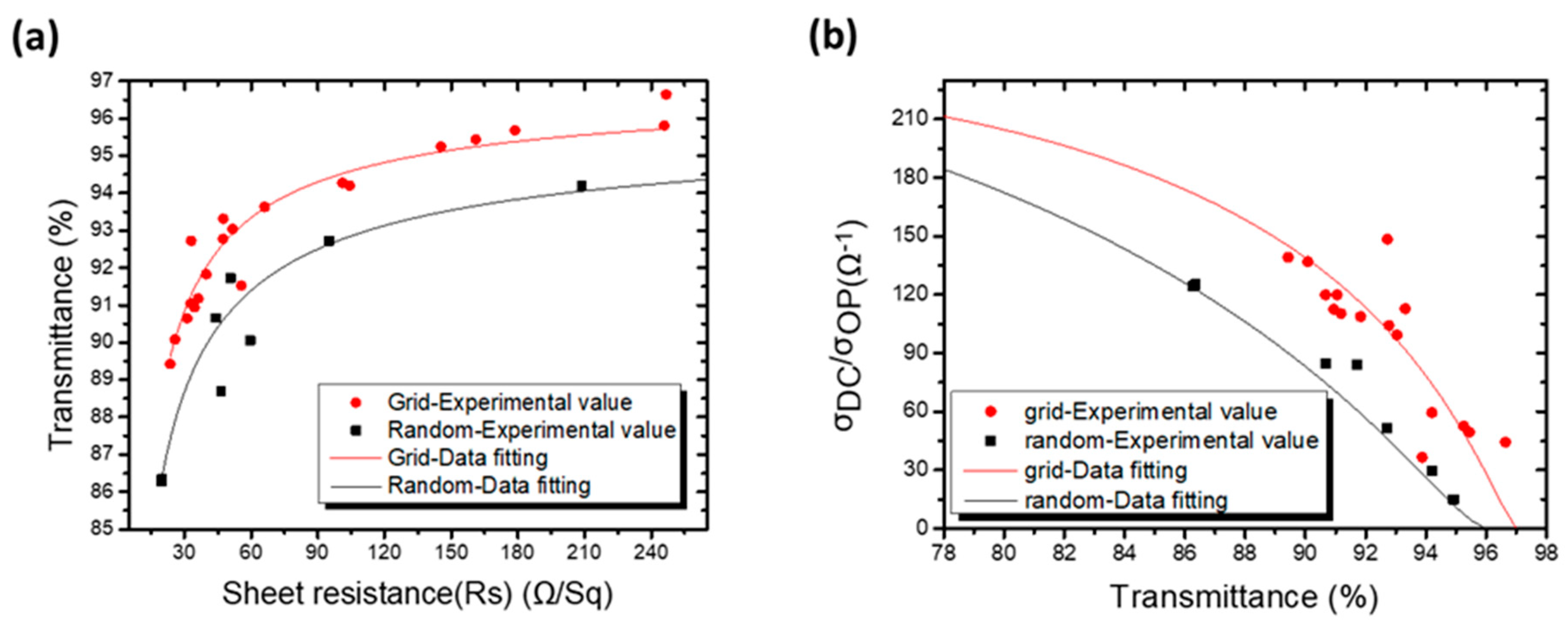
3.5. Performance of Grid-Structured AgNW Electrodes

The expanded images of the randomly deposited and grid-patterned AgNW films are shown in Figure 6. Large junctions and dense bundles of AgNWs can be observed in the grid-patterned AgNW film, unlike in the random film. The difference in the structures between these films resulted in differences in their performance as transparent electrodes. The AgNW electrode with a grid structure has bundles of AgNWs on all sides of the grid and junctions at the intersection of the grid. The bundles and junctions offer many points of contact for the AgNWs; they facilitate many electron movement paths and lower the sheet resistance of the electrode. The AgNWs are well structured along the grid-patterned area with an average thickness of 130.5 nm (Figure 6f). In addition, owing to the open space of the grid structure, grid-structured AgNW film has higher transmittance than the randomly networked AgNW film.
Consequently, the grid-structured AgNW film can display superior performance to that of the randomly deposited AgNW films, as shown in Figure 7. The grid-structured films have higher transmittance than the randomly deposited films at the same sheet resistance value. The dots represent the experimental values of transmittance at a wavelength of 550 nm and sheet resistance. The smooth line was obtained through nonlinear curve fitting. The fitted equations of both curves express the transmittance (T) as a function of the sheet resistance ( R s h ) (Equations (2) and (3)).
T G r i d = 0.96 0.81 R s h 0.76
T R a n d o m = 0.96 0.67 R s h 0.64
In general, the transmittance and sheet resistance can be related to a figure-of-merit (FoM), which is defined as the electrical conductivity-to-optical conductivity ratio (Equation (4)) [36].
T = ( 1 + 188.5 R s h σ O P σ D C ) 2
where σ D C is the electrical conductivity and σ O P is the optical conductivity of the conductive film.
The value of σ O P σ D C is called the FoM, and it is used for the quantitative analysis of the performance of thin transparent electrodes. The higher the FoM is, the better the transparent conductive electrode is. By fitting the experimental values to Equation (4), the FoM values of the grid-structured and randomly deposited AgNW films were determined to be 118 and 108, respectively. We can confirm that the performance of the grid-structured film as a TCE is better than that of the randomly deposited grid, because the FoM value of the former is 13% higher than that of the latter. Figure 7 illustrates the relationship between the transmittance and FoM for the grid-structured and randomly deposited films. The FoM value of the grid-structured film is higher for the overall transmittance.
The percolation threshold theory also supports this result. According to this theory, interconnections between neighboring wires of small dimensions can form larger groups over a surface if the 2D surface concentration reaches a specific threshold that is large enough so that any potential boundary effect can be negligible [37], and this point is called the percolation threshold. Equation (5) expresses the theory by relating the sheet resistance and surface concentration.
R s h = A ( X X c ) α
where X is the surface concentration of AgNWs, X c is the percolation threshold, and α is the percolation exponent, which is correlated to the dimensionality of the percolated film.
To obtain the relationship between the transmittance and surface concentration, a controlled amount of AgNW was deposited by continuous back and forth dragging of deposition plate until the solvent was completely vaporized during the MDD, depositing all injected amount of AgNWs. The transmittance was then measured, and the surface concentration was calculated; they were then related by a linear fit. These are shown in Figure 8.
A nonlinear curve fitting was performed to estimate the percolation threshold of each electrode (Figure 8). The estimated percolation exponent ( α ) values are 1.33 (grid) and 1.31 (random), which are very close to the theoretical value of the 2D model ( α = 1.33 ) . The percolation threshold of the grid-patterned electrode ( X c = 1.246 ) is much lower than that of the randomly deposited one ( X c = 2.944 ) , implying that the grid-patterned electrode is more AgNW-efficient. Finally, Figure 9 compares the optoelectrical properties of our AgNW grid film with those of other AgNW conductive films [8,38,39,40,41]. Our AgNW grid film exhibits good performance over a wide range of transmittance values.

4. Conclusions

In this study, AgNW films with a grid structure were formed by the MDD, which is the efficient method for fabricating random networks. An AgNW suspension containing EG was used to form a thin liquid film on the selectively hydrophilized substrate surface with OTS. The EG concentration increased as IPA vaporized, and the surface tension of the film increased. The high surface tension of liquid film and surface energy gradation of OTS patterned substrate results in pre-programmed dewetting of liquid thin film, creating grid-patterned AgNW electrodes. Various structures of AgNWs were formed by controlling the EG concentration of the coating mixture and the coating parameters. The fabricated grid structure of the AgNW film exhibits competitive conductivity and transmittance than those from recently reported AgNW based electrodes. Therefore, we expect our works will contribute to wide-spread utilization of Ag NW as a transparent electrode, replacing ITO.

Author Contributions

Conceptualization, J.Y. and S.T.C.; Methodology, J.Y. and S.M.L.; Validation, J.Y., S.M.L., H.-S.E., and S.T.C.; Investigation, J.Y. and S.M.L.; Resources, J.Y. and S.T.C.; Data Curation, J.Y., S.M.L., and S.T.C.; Writing—Original Draft Preparation, J.Y. and S.M.L.; Writing—Review & Editing, J.Y., S.M.L., H.-S.E., and S.T.C.; Supervision, S.T.C.; Project Administration, S.T.C.; Funding Acquisition, S.T.C. All authors have read and agreed to the published version of the manuscript.

Funding

This research was supported by the National Research Foundation of Korea (NRF) grant funded by the Korean government (No. 2019R1A2C1006413) and the Chung-Ang University Research Scholarship Grants in 2019.

Data Availability Statement

Data is contained within the article.

Conflicts of Interest

The authors declare no conflict of interest.

References

  1. He, L.; Tjong, S.C. Nanostructured transparent conductive films: Fabrication, characterization and applications. Mater. Sci. Eng. R Rep. 2016, 109, 1–101. [Google Scholar] [CrossRef]
  2. Pang, S.; Hernandez, Y.; Feng, X.; Müllen, K. Graphene as transparent electrode material for organic electronics. Adv. Mater. 2011, 23, 2779–2795. [Google Scholar] [CrossRef] [PubMed]
  3. Lu, S.-K.; Huang, J.-T.; Lee, T.-H.; Wang, J.-J.; Liu, D.-S. Flexibility of the indium tin oxide transparent conductive film deposited onto the plastic substrate. Smart Sci. 2014, 2, 7–12. [Google Scholar] [CrossRef]
  4. Liu, Y.; Li, Y.; Zeng, H. ZnO-based transparent conductive thin films: Doping, performance, and processing. J. Nanomater. 2013, 2013, 196521. [Google Scholar] [CrossRef] [Green Version]
  5. Liu, H.; Liu, Y.-F.; Xiong, P.-P.; Chen, P.; Li, H.-Y.; Hou, J.-W.; Kang, B.-N.; Duan, Y. Aluminum-doped zinc oxide transparent electrode prepared by atomic layer deposition for organic light emitting devices. IEEE Trans. Nanotechnol. 2017, 16, 634–638. [Google Scholar] [CrossRef]
  6. Dan, B.; Irvin, G.C.; Pasquali, M. Continuous and scalable fabrication of transparent conducting carbon nanotube films. ACS Nano 2009, 3, 835–843. [Google Scholar] [CrossRef] [PubMed] [Green Version]
  7. Wu, Z.; Chen, Z.; Du, X.; Logan, J.M.; Sippel, J.; Nikolou, M.; Kamaras, K.; Reynolds, J.R.; Tanner, D.B.; Hebard, A.F. Transparent, conductive carbon nanotube films. Science 2004, 305, 1273–1276. [Google Scholar] [CrossRef]
  8. Ko, Y.U.; Cho, S.-R.; Choi, K.S.; Park, Y.; Kim, S.T.; Kim, N.H.; Kim, S.Y.; Chang, S.T. Microlitre scale solution processing for controlled, rapid fabrication of chemically derived graphene thin films. J. Mater. Chem. 2012, 22, 3606–3613. [Google Scholar] [CrossRef]
  9. Layani, M.; Darmawan, P.; Foo, W.L.; Liu, L.; Kamyshny, A.; Mandler, D.; Magdassi, S.; Lee, P.S. Nanostructured electrochromic films by inkjet printing on large area and flexible transparent silver electrodes. Nanoscale 2014, 6, 4572–4576. [Google Scholar] [CrossRef]
  10. Guo, H.; Lin, N.; Chen, Y.; Wang, Z.; Xie, Q.; Zheng, T.; Gao, N.; Li, S.; Kang, J.; Cai, D. Copper nanowires as fully transparent conductive electrodes. Sci. Rep. UK 2013, 3, 1–8. [Google Scholar] [CrossRef] [Green Version]
  11. Ko, Y.; Song, S.K.; Kim, N.H.; Chang, S.T. Highly transparent and stretchable conductors based on a directional arrangement of silver nanowires by a microliter-scale solution process. Langmuir 2016, 32, 366–373. [Google Scholar] [CrossRef] [PubMed]
  12. Nguyen, Q.; Kwon, J.W. Silver nanowire-based transparent electrode as FTO replacement for dye-sensitized solar cell. Int. Nano Lett. 2019, 9, 83–87. [Google Scholar] [CrossRef] [Green Version]
  13. Gebeyehu, M.B.; Chala, T.F.; Chang, S.-Y.; Wu, C.-M.; Lee, J.-Y. Synthesis and highly effective purification of silver nanowires to enhance transmittance at low sheet resistance with simple polyol and scalable selective precipitation method. RSC Adv. 2017, 7, 16139–16148. [Google Scholar] [CrossRef] [Green Version]
  14. Korte, K.E.; Skrabalak, S.E.; Xia, Y. Rapid synthesis of silver nanowires through a CuCl-or CuCl2-mediated polyol process. J. Mater. Chem. 2008, 18, 437–441. [Google Scholar] [CrossRef]
  15. Yun, H.D.; Seo, D.M.; Lee, M.Y.; Kwon, S.Y.; Park, L.S. Effective synthesis and recovery of silver nanowires prepared by tapered continuous flow reactor for flexible and transparent conducting electrode. Metals-Basel 2016, 6, 14. [Google Scholar] [CrossRef] [Green Version]
  16. Xie, S.; Ouyang, Z.; Jia, B.; Gu, M. Large-size, high-uniformity, random silver nanowire networks as transparent electrodes for crystalline silicon wafer solar cells. Opt. Express 2013, 21, A355–A362. [Google Scholar] [CrossRef]
  17. Lee, C.; Oh, Y.; Yoon, I.S.; Kim, S.H.; Ju, B.-K.; Hong, J.-M. Flash-induced nanowelding of silver nanowire networks for transparent stretchable electrochromic devices. Sci. Rep. UK 2018, 8, 1–10. [Google Scholar] [CrossRef] [Green Version]
  18. Xiong, W.; Liu, H.; Chen, Y.; Zheng, M.; Zhao, Y.; Kong, X.; Wang, Y.; Zhang, X.; Kong, X.; Wang, P. Highly conductive, air-stable silver nanowire@ iongel composite films toward flexible transparent electrodes. Adv. Mater. 2016, 28, 7167–7172. [Google Scholar] [CrossRef]
  19. Correa, D.; Medeiros, E.; Oliveira, J.; Paterno, L.; Mattoso, L.H. Nanostructured conjugated polymers in chemical sensors: Synthesis, properties and applications. J. Nanosci. Nanotechnol. 2014, 14, 6509–6527. [Google Scholar] [CrossRef]
  20. Li, Y.; Yuan, X.; Yang, H.; Chao, Y.; Guo, S.; Wang, C. One-step synthesis of silver nanowires with ultra-long length and thin diameter to make flexible transparent conductive films. Materials 2019, 12, 401. [Google Scholar] [CrossRef] [Green Version]
  21. Seok, H.-J.; Kim, J.-K.; Kim, H.-K. Effective passivation of Ag nanowire network by transparent tetrahedral amorphous carbon film for flexible and transparent thin film heaters. Sci. Rep. UK 2018, 8, 1–12. [Google Scholar] [CrossRef] [PubMed]
  22. Yoon, J.-W.; Chang, W.S.; Cho, S.H. Laser direct patterning of AgNW/CNT hybrid thin films. Opt. Laser. Eng. 2015, 73, 40–45. [Google Scholar] [CrossRef]
  23. Lee, M.-S.; Kim, J.; Park, J.; Park, J.-U. Studies on the mechanical stretchability of transparent conductive film based on graphene-metal nanowire structures. Nanoscale. Res. Lett. 2015, 10, 27. [Google Scholar] [CrossRef] [PubMed] [Green Version]
  24. Xu, Q.; Song, T.; Cui, W.; Liu, Y.; Xu, W.; Lee, S.-T.; Sun, B. Solution-processed highly conductive PEDOT: PSS/AgNW/GO transparent film for efficient organic-Si hybrid solar cells. ACS Appl. Mater. Interfaces 2015, 7, 3272–3279. [Google Scholar] [CrossRef] [PubMed]
  25. Lee, Y.; Min, S.Y.; Kim, T.S.; Jeong, S.H.; Won, J.Y.; Kim, H.; Xu, W.; Jeong, J.K.; Lee, T.W. Versatile metal nanowiring platform for large-scale nano-and opto-electronic devices. Adv. Mater. 2016, 28, 9109–9116. [Google Scholar] [CrossRef] [PubMed]
  26. Liu, G.-S.; Liu, C.; Chen, H.-J.; Cao, W.; Qiu, J.-S.; Shieh, H.-P.D.; Yang, B.-R. Electrically robust silver nanowire patterns transferrable onto various substrates. Nanoscale 2016, 8, 5507–5515. [Google Scholar] [CrossRef] [PubMed]
  27. Kim, S.; Kim, B.; Cho, S.M.; Lee, H.-J.; Hwang, B. Etchant-free patterning of silver nanowire transparent electrode using dry-film photoresists for organic light-emitting diodes. Mater. Lett. 2017, 209, 433–436. [Google Scholar] [CrossRef]
  28. Ko, D.; Gu, B.; Kang, S.J.; Jo, S.; Hyun, D.C.; Kim, C.S.; Kim, J. Critical work of adhesion for economical patterning of silver nanowire-based transparent electrodes. J. Mater. Chem. A 2019, 7, 14536–14544. [Google Scholar] [CrossRef]
  29. Liao, Q.; Wang, H.; Zhu, X.; Li, M. Liquid droplet movement on horizontal surface with gradient surface energy. Sci. China Ser. E 2006, 49, 733–741. [Google Scholar] [CrossRef]
  30. Calvert, J.; Georger, J.; Schnur, J.; Schoen, P.; Peckerar, M.; Pehrsson, P. Deep UV photochemistry and patterning of self-assembled monolayer films. Thin Solid Film. 1992, 210, 359–363. [Google Scholar] [CrossRef]
  31. Lee, S.M.; Oh, S.; Chang, S.T. Highly transparent, flexible conductors and heaters based on metal nanomesh structures manufactured using an all-water-based solution process. ACS Appl. Mater. Interfaces 2019, 11, 4541–4550. [Google Scholar] [CrossRef] [PubMed]
  32. Sett, S.; Yan, X.; Barac, G.; Bolton, L.W.; Miljkovic, N. Lubricant-infused surfaces for low-surface-tension fluids: Promise versus reality. ACS. Appl. Mater. Interfaces 2017, 9, 36400–36408. [Google Scholar]
  33. Li, Q.; Zhou, P.; Yan, H. Pinning–depinning mechanism of the contact line during evaporation on chemically patterned surfaces: A lattice Boltzmann study. Langmuir 2016, 32, 9389–9396. [Google Scholar] [CrossRef] [PubMed]
  34. Kim, N.H.; Kim, B.J.; Ko, Y.; Cho, J.H.; Chang, S.T. Surface energy engineered, high-resolution micropatterning of solution-processed reduced graphene oxide thin films. Adv. Mater. 2013, 25, 894–898. [Google Scholar] [CrossRef] [PubMed]
  35. Budiman, A.G.; Florijanto, C.; Palen, J. Breakdown of evaporating falling films as a function of surface tension gradient. Heat Transf. Eng. 1996, 17, 72–81. [Google Scholar] [CrossRef]
  36. Sepulveda-Mora, S.B.; Cloutier, S.G. Figures of merit for high-performance transparent electrodes using dip-coated silver nanowire networks. J. Nanomater. 2012, 2012, 286104. [Google Scholar] [CrossRef]
  37. Bellet, D.; Lagrange, M.; Sannicolo, T.; Aghazadehchors, S.; Nguyen, V.H.; Langley, D.P.; Muñoz-Rojas, D.; Jiménez, C.; Bréchet, Y.; Nguyen, N.D. Transparent electrodes based on silver nanowire networks: From physical considerations towards device integration. Materials 2017, 10, 570. [Google Scholar] [CrossRef]
  38. Xiong, J.; Li, S.; Ye, Y.; Wang, J.; Qian, K.; Cui, P.; Gao, D.; Lin, M.F.; Chen, T.; Lee, P.S. A deformable and highly robust ethyl cellulose transparent conductor with a scalable silver nanowires bundle micromesh. Adv. Mater. 2018, 30, 1802803. [Google Scholar] [CrossRef]
  39. Kim, S.; Kim, S.Y.; Kim, J.; Kim, J.H. Highly reliable AgNW/PEDOT: PSS hybrid films: Efficient methods for enhancing transparency and lowering resistance and haziness. J. Mater. Chem. C 2014, 2, 5636–5643. [Google Scholar] [CrossRef]
  40. Ramadhan, Z.R.; Han, J.W.; Lee, D.J.; Entifar, S.A.N.; Hong, J.; Yun, C.; Kim, Y.H. Surface-functionalized silver nanowires on chitosan biopolymers for highly robust and stretchable transparent conducting films. Mater. Res. Lett. 2019, 7, 124–130. [Google Scholar] [CrossRef]
  41. Su, Q.; Xue, T.; Zhang, Y.; Lan, K.; Zou, Q. Fabrication of enhanced silver nanowire films via self-assembled gold nanoparticles without post-treatment. Mater. Lett. 2019, 236, 218–221. [Google Scholar] [CrossRef]
Figure 1. A schematic illustration of the fabrication of a grid-patterned silver nanowire (AgNW) film.
Coatings 11 00030 g001
Figure 2. Optical microscopic images of AgNW grid structures with widths and spacings of (a) 1 and 40 μm, (b) 2 and 40 μm, (c) 5 and 40 μm, and (d) 10 and 40 μm.
Coatings 11 00030 g002
Figure 3. Optical microscopic images of AgNW grids obtained by coating at different deposition velocities (DVs): (a) 0.17, (b) 1, (c) 2, and (d) 3 cm/s.
Coatings 11 00030 g003
Figure 4. Transmittance and sheet resistance of AgNW grids fabricated by coating (a) at different DVs and (b) with different concentrations of ethylene glycol in the solution. The corresponding UV-vis spectrum with respect to (c) the deposition velocity and (d) ethylene glycol (EG) EG concentration.
Coatings 11 00030 g004
Figure 5. Optical microscopic images of AgNW grids fabricated by coating using mixtures with different EG concentrations: (a) 0.1, (b) 0.3, (c) 0.5, and (d) 1 vol.%.
Coatings 11 00030 g005
Figure 6. Optical microscopic images of the (a) randomly deposited AgNW film and (c) grid-patterned AgNW film. FE-SEM images of the (b) randomly deposited AgNW film, (d) grid-patterned AgNW film, and (e) parts of the grid structure. (f) AFM images of bundled AgNWs in grid-structured AgNW film and corresponding height profile.
Coatings 11 00030 g006
Figure 7. (a) The transmittance at 550 nm versus sheet resistance for gird-patterned AgNW electrodes and randomly networked AgNW electrodes and (b) the figure-of-merit (FOM) versus transmittance at 550 nm for the grid-patterned electrodes and randomly networked AgNW electrodes.
Coatings 11 00030 g007
Figure 8. (a) Linear relationship between the transmittance and surface concentration. (b) Relationship between the sheet resistance and surface concentration fitted with a nonlinear curve.
Coatings 11 00030 g008
Figure 9. Comparison of the grid-structured AgNWs electrode and other AgNW conductive films in optoelectrical conductivity.
Coatings 11 00030 g009
Publisher’s Note: MDPI stays neutral with regard to jurisdictional claims in published maps and institutional affiliations.

