Article

Effects of O2 Plasma Treatments on the Photolithographic Patterning of PEDOT:PSS

1
Institute of Photonics Technologies, Department of Electrical Engineering, National Tsing Hua University, 101 Sec. 2 Kuang-Fu Road, Hsinchu 30013, Taiwan
2
Department of Physics, National Tsing Hua University, 101 Sec. 2 Kuang-Fu Road, Hsinchu 30013, Taiwan
*
Author to whom correspondence should be addressed.
Coatings 2021, 11(1), 31; https://doi.org/10.3390/coatings11010031
Submission received: 14 November 2020 / Revised: 21 December 2020 / Accepted: 21 December 2020 / Published: 30 December 2020
(This article belongs to the Special Issue Selected Papers from the IIKII 2020&2021 Conferences)

Abstract

:
Poly (3,4-ethylenedioxythiophene) polystyrene sulfonate (PEDOT:PSS) is known for its potential to replace indium–tin oxide in various devices. Herein, when fabricating finger-type PEDOT:PSS electrodes using conventional photolithography, the cross-sectional profiles of the patterns are U-shaped instead of rectangular. The films initially suffer from non-uniformity and fragility as well as defects owing to undesirable patterns. Adding a small amount of hydrolyzed silane crosslinker to PEDOT:PSS suspensions increases the mechanical durability of PEDOT:PSS patterns while lifting off the photoresist. To further improve their microfabrication, we observe the effects of two additional oxygen (O2) plasma treatments on conventional photolithography processes for patterning PEDOT:PSS, expecting to observe how O2 plasma increases the uniformity of the patterns and changes the thickness and U-shaped cross-sectional profiles of the patterns. Appropriately exposing the patterned photoresist to O2 plasma before spin-coating PEDOT:PSS improves the wettability of its surface, including its sidewalls, and a similar treatment before lifting off the photoresist helps partially remove the spin-coated PEDOT:PSS that impedes the lift-off process. These two additional processes enable fabricating more uniform, defect-free PEDOT:PSS patterns. Both increasing the wettability of the photoresist patters before spin-coating PEDOT:PSS and reducing its conformal coverage are key to improving the photolithographic microfabrication of PEDOT:PSS.

Graphical Abstract

1. Introduction

Advancing terahertz (THz) technology [1,2] requires developing many functional quasi-optical components for THz devices such as phase shifters [3,4,5,6,7,8], filters [9], phase gratings [10], and polarizers [11]; however, most of these device components use indium–tin oxide (ITO) or metal electrodes, the transmittance of which is not necessarily high enough for THz devices.
To improve transmittance characteristics, on one hand, finger-type ITO electrodes [12], which mitigate the absorption of light via ITO, have been fabricated by patterning flat ITO electrodes. On the other hand, materials with higher transmittance in the THz region such as graphene [13] are actively being attempted to replace ITO. For this purpose, poly(3,4-ethylenedioxythiophene) polystyrene sulfonate (PEDOT:PSS) [14,15,16,17,18,19] is a promising candidate, and patterning PEDOT:PSS as a microfabrication strategy has been well studied. PEDOT:PSS exhibits high transmittance in the THz region, and because of its solution-process capability, it can be patterned using photolithography. Under these circumstances, replacing the finger-type ITO electrodes with patterned PEDOT:PSS ones would attain even higher transmittance in the THz region. Therefore, we attempted to fabricate finger-type electrodes using PEDOT:PSS; however, the films suffered from non-uniformity and fragility as well as defects owing to undesirable patterns.
As wearable and portable electronics have continued to develop [20], PEDOT:PSS as a flexible transparent electrode has been gaining an important role in such optoelectronic devices [21]. For practical purposes, developing versatile patterning techniques is required for incorporating PEDOT:PSS into these optoelectronic devices. Micropatterning has been developed for organic materials, but some challenges have not yet been fully addressed; in particular, the surface morphology and electrical and optical properties of patterned PEDOT:PSS are adversely influenced by patterning processes. This is because organic materials, i.e., soft matter, that can be dissolved or dispersed in water or organic solvents are usually mechanically fragile and chemically sensitive. These difficulties have encouraged researchers to devise various approaches in different micro- and nanopatterning techniques to solve these problems and to ultimately achieve well-organized, uniformly patterned surfaces with fine structures.
In principle, photolithography is applicable to organic materials including PEDOT:PSS when the proper materials and processes are selected [16]. Traditional photolithography materials and processes can be used in the lift-off process. As another alternative method, using orthogonal solvents and corresponding photoresists enables creating submicrometer-scale PEDOT:PSS patterns [22,23]; however, they can potentially be damaged by aggressive organic solvents. In addition, PEDOT:PSS can be directly crosslinked by ultraviolet (UV) irradiation with an appropriate photoinitiator [24,25,26], but the resolution is limited to several micrometers. From the above-mentioned techniques, we choose traditional photolithography together with the lift-off process. In other words, we observe how PEDOT:PSS films can be patterned using traditional photolithography and how undesirable patterns or defects, if any, made by photolithographic processes can be altered and improved.
Plasma treatments are well known and offer many advantages in fabrication processes because they can modify the surface properties, but exposing a surface to plasma does not alter its bulk properties [27]. Plasma treatment can prime any surface for secondary manufacturing processes by eliminating all traces of contamination. Therefore, we are interested in observing the correlation between plasma treatments and the surface structures and morphologies of photolithographic PEDOT:PSS patterns while exploring ways to improve their quality.
In this study, we aim to tackle the aforementioned problems, i.e., the non-uniformity and fragility of the films as well as defects owing to undesirable patterns, and to improve the quality of photolithographic PEDOT:PSS patterns. Although photolithography has already been established for PEDOT:PSS, some material- and process-related factors seem to affect the quality of the films and patterns. For this purpose, we introduce two additional O2 plasma processes into traditional photolithography, and we analyze how each additional plasma treatment affects the PEDOT:PSS patterns, expecting to improve them by applying these two additional processes. From a practical perspective, exploiting these basic, unsophisticated fabrication processes while unveiling their effects helps further develop the photolithographic patterning of PEDOT:PSS thin films in a facile, familiar way.

2. Materials and Methods

2.1. Materials and Procedure

Soda-lime glass substrates with dimensions of 25 × 25 × 0.7 mm were sequentially sonicated in commercially available detergent RBS™ 35 Concentrate (Thermo Fisher Scientific, Waltham, MA, USA) and deionized water (>18 MΩ·cm) for 15 min. To increase its hydrophilicity, the surface of the substrates was exposed to O2 plasma with a power of 100 W and O2 flowing at 15 sccm for 3 min using a Samco-ucp PC-300 plasma cleaner (Ruggell, Liechtenstein). A positive photoresist AZ4620 (Merck KGaA, Darmstadt, Germany) was spin-coated onto the substrates at 4000 rpm for 40 s and then baked at 90 °C for 7 min. The photoresist films were exposed to UV light for 7 s using an EVG®620 mask aligner. The photoresist films were developed in a developer solution AD-10 (Merck KGaA, Darmstadt, Germany) for 3 min.
Figure 1 illustrates the designed mask patterns of a unit cell together with an enlarged diagram of a corner of the electrode area showing a part of the finger-type electrodes near the edge. The total electrode dimensions are 14 × 13 mm, and each finger-type electrode is 20 µm wide with a 20 µm gap between neighboring electrodes. In practice, the four designed unit cells were laid out in a soda-lime mask with dimensions of 5 × 5 × 0.09 in (12.7 × 12.7 × 0.229 cm).
A PEDOT:PSS dispersion (PH1000, Heraeus Epurio Clevios™, Leverkusen, Germany) was filtered through a 0.45 μm syringe filter and then mixed with 0.2 wt % (3-glycidyloxypropyl)trimethoxysilane (GOPS) [28,29], a hydrolyzed silane crosslinker (Sigma-Aldrich, St. Louis, MO, USA). The suspension was sonicated for 30 min to homogenize the PEDOT:PSS dispersion, which was then spin-coated at 3000 rpm for 60 s onto the patterned photoresist. The spin-coated substrates were baked at 130 °C for 15 min and finally sonicated in acetone to lift off the photoresist.
In our modified process, two O2 plasma treatments were independently added, one before spin-coating PEDOT:PSS and one before lifting off the photoresist. The O2 plasma power and the O2 flow rate were set to 100 W and 15 sccm, respectively, for both reactive-ion etching (RIE) and plasma etching (PE) modes, and each operation time was varied. The latter mode is more isotropic and gentler, whereas in the former mode, the O2 species are generated more vertically and hit the substrates more vigorously because of the potential between the electrodes in the chamber.

2.2. Measurements

A Dimension ICON scanning probe microscope system (Bruker, Billerica, MA, USA), which offers precisions of <0.15 Å nm for XY noise and <0.35 Å Z sensor noise, was used to measure the film thickness and probe its height profiles on the surface of the substrates. We prepared three samples for each set of conditions. For each sample, we measured at least three points in the upper, middle, and lower parts of the electrode area shown in Figure 1, and we measured each point three times. We also used a Quatek (Sheung Wan, Hong Kong) four-point probe test system, composed of a 5601TSR surface resistance tester and a QT-50 manual test console, to measure the surface resistance Rs(Ω) of films, from which the conductivity σ (S/cm) = 1/(Rs·d) was deduced using the film thickness d (cm).

3. Results

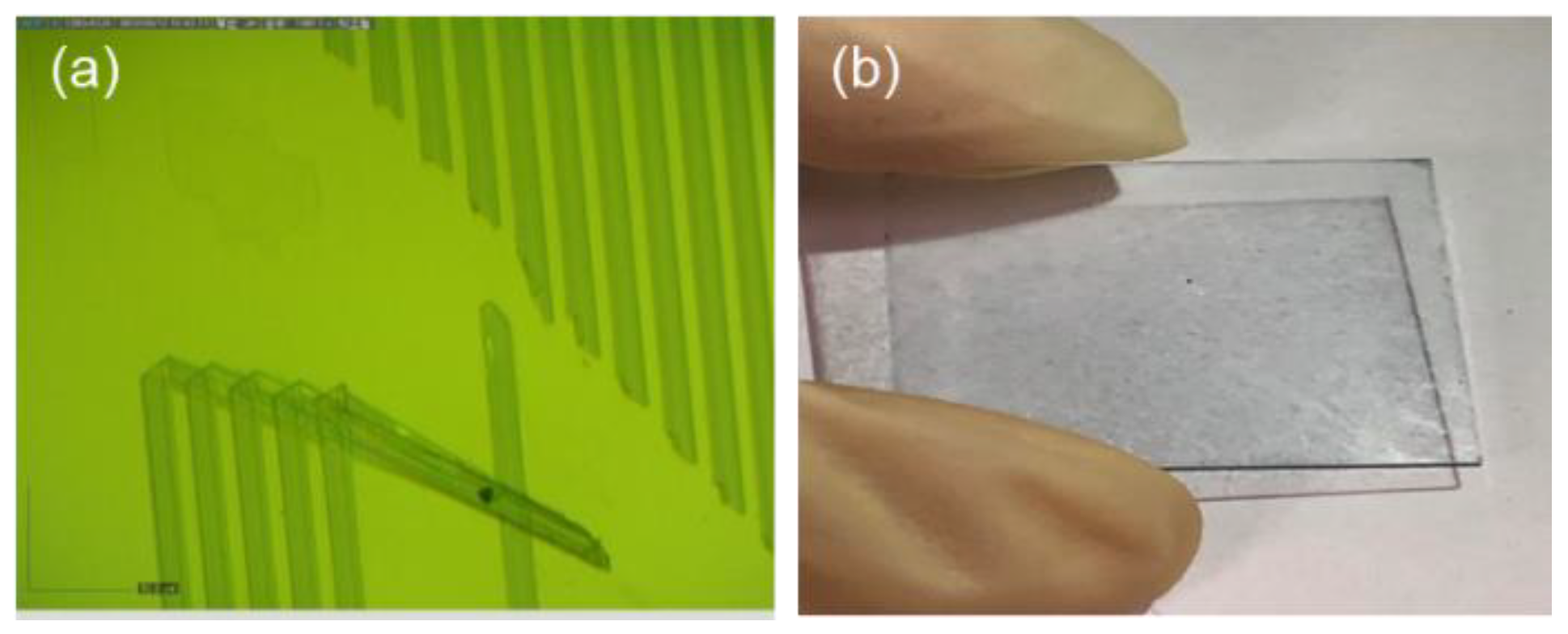
3.1. Transferring an Image to the Photoresist and the Fragility of PEDOT:PSS Patterns

To draw a finger-type (stripe-type) image on the photoresist, a mask pattern (design drawing or pattern) is first transferred. The stripe-type-patterned photoresist works as a template or mold to create PEDOT:PSS patterns [16,30]. To this end, some process conditions are optimized using various quality engineering methods [31], i.e., by controlling the spin-coating rotational speed, baking temperature, UV-light-exposure time, and developing time, as described in the experimental section. Using these optimized conditions, we attain a high-quality patterned photoresist, and the patterns are transferred from the mask patterns with a gap of 20 µm between neighboring patterns. By using the image (pattern) of the photoresist, PEDOT:PSS is then patterned via microprocessing.
Initially, the PEDOT:PSS patterns were very mechanically fragile, especially in the lift-off process, during which the substrates were shaken in an acetone bath. To remove the photoresist patterns from the substrates, they were inevitably shaken, which presumably applied a frictional force to the PEDOT:PSS patterns on the substrates. In fact, the PEDOT:PSS patterns were partially peeled off and bent out of the substrates, as shown in Figure 2. Simply immersing substrates in acetone, however, does not remove photoresist patterns from substrates; therefore, to avoid damaging the patterns, the films had to be strengthened. This fragility can be attributed to the weak anchoring of the PEDOT:PSS films to the surface of the substrates, although this technique is well known [28,29,32]. However, exposing the photoresist patterns to O2 plasma did not mitigate this problem, so it had to be resolved using surfactants.
Specifically, GOPS, a hydrolyzed silane crosslinker, was used to improve the anchoring, as its epoxy group can react open under acidic conditions, yielding a hydroxyl group. When GOPS is added to PEDOT:PSS suspensions, the hydroxyl groups strongly interact with the sulfonic acid groups of PEDOT:PSS via hydrogen bonds. The trimethoxysilane groups of GOPS are hydrolyzed in acidic suspensions and become Si–OH groups, which form stable Si–O–Si bonds on the glass surface [32]. To reveal the effects of GOPS in the PEDOT:PSS suspensions, its concentration was varied, and the durability of the resulting PEDOT:PSS patterns was evaluated. As the GOPS concentration increased, fewer defects ended to appear in the PEDOT:PSS patterns. However, 3.0 wt % GOPS caused PEDOT:PSS to agglomerate, which was previously reported to hinder spin-coating [29]. Further, we confirmed that adding GOPS decreased the conductivity of the PEDOT:PSS films, suggesting a trade-off relationship between improving the durability and maintaining the conductivity of the PEDOT:PSS films. Figure 3 shows the relationship between the conductivity of PEDOT:PSS films and the GOPS concentration, which shows almost the same trend as that observed in previous work [28], although the initial conductivity without GOPS was slightly lower here. Based on these findings, we used 0.2 wt % GOPS in subsequent experiments because this concentration yielded PEDOT:PSS films that were sufficiently durable during the lift-off process.

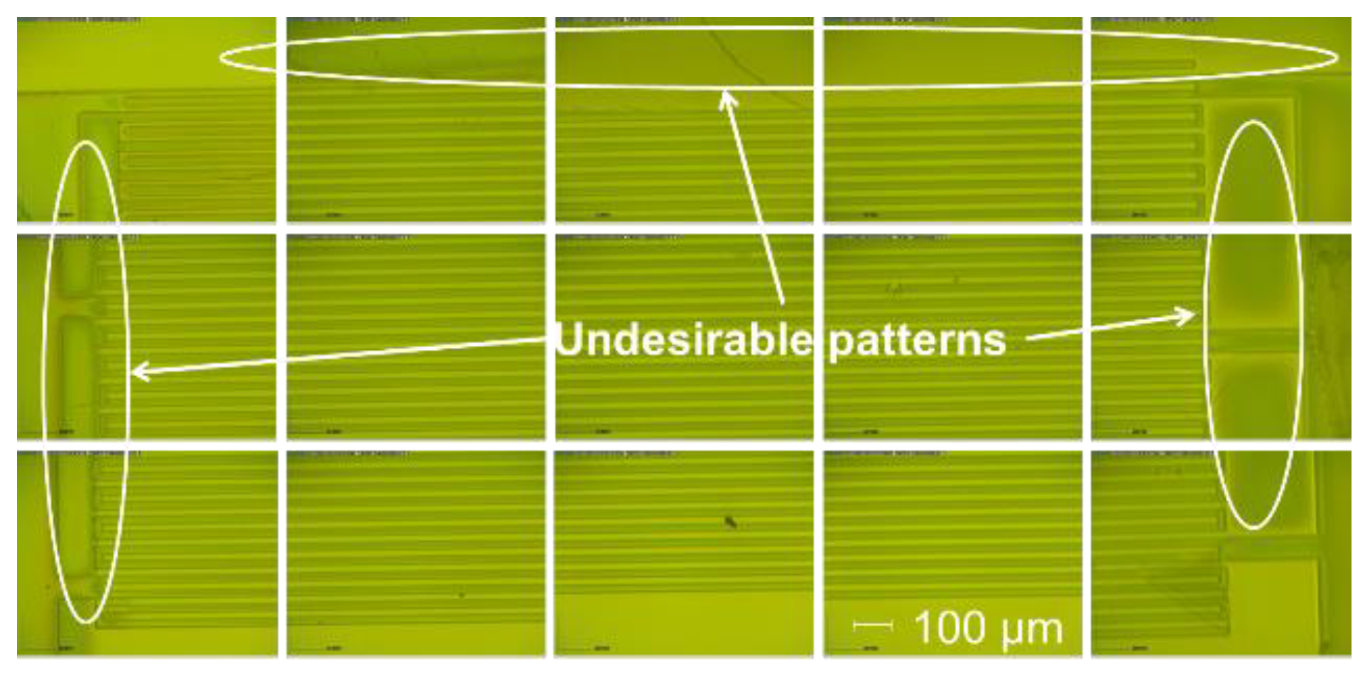
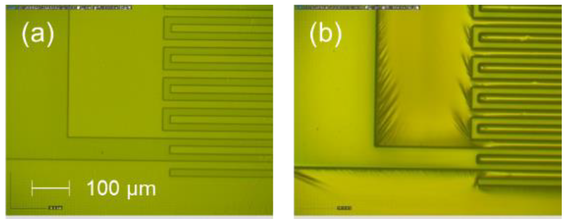
3.2. Traditional Process for PEDOT:PSS

Figure 4 shows the two-dimensional height profiles of the PEDOT:PSS patterns obtained using the traditional process. Each sample was measured at several points in the sample, and an average was taken at each position. Considering the photoresist patterns, we expect to observe a rectangular cross-section with a line width of 20 μm. Surprisingly, however, the actual profiles are U-shaped [33,34], with large variations in thickness at the center of the lines. The U-shaped profiles could be attributed to the evaporation of solvent and its corollary mass transfer [35]. If the surface of the photoresist has good wettability, the suspension spreads not only in the planar direction but also upward along the sidewalls of the photoresist. In addition, as the solvent evaporates, mass transfer occurs at the edge of the suspension on the sidewall of the photoresist, thereby leading to the U-shaped profiles at the edge. According to this mechanism, a higher concentration with higher viscosity would reduce the peak height of the U-shaped profiles, whereas better wettability, including on the sidewalls of the photoresist, would develop U-shaped profiles.
From another perspective, the bottom of the lines is approximately 30 μm, which is 1.5 times larger than the designed value. In contrast, the peak-to-peak width is almost 20 μm, suggesting that each peak must be determined by the sidewall of the patterned photoresist. Presumably, when PEDOT:PSS is spin-coated onto the patterned photoresist, PEDOT:PSS not only fills the spaces between the lines of the patterned photoresist but also covers the top of the photoresist. The PEDOT:PSS initially present on top of the photoresist can be connected to the PEDOT:PSS between the lines via conformal coverage. Therefore, even after the photoresist patterns are removed during the lift-off process, partially connected PEDOT:PSS would remain at the bottom of the patterns [30]. These observations suggest that removing the PEDOT:PSS from the top of the photoresist may help improve the quality and uniformity of the final PEDOT:PSS patterns.

3.3. Adding an O2 Plasma Treatment before Spin-Coating

O2 plasma increases the hydrophilicity of surfaces. Contact angle measurements revealed that the surface of the patterned photoresist was rather hydrophobic, which prompted us to add an O2 plasma treatment before spin-coating PEDOT:PSS, which would also remove the PEDOT:PSS from the top of the patterned photoresist. Figure 5 shows how PEDOT:PSS suspensions spread on the surface of the photoresist with and without an O2 plasma treatment; clearly, increasing the O2 plasma operation time further increased the wettability of the patterned photoresist surface.
We found that adding the O2 plasma treatment at this point during processing indeed improves the uniformity of the thickness. Figure 6 shows how the height profiles of the cross-sectional PEDOT:PSS patterns change when the patterned photoresist is plasma-treated in RIE mode before spin-coating it with PEDOT:PSS. As the operating time of the O2 plasma treatment increases, the center of the lines becomes more uniform. Interestingly, however, the peaks that appear at the edge of each line become more pronounced with the increasing operating time, which suggests that the plasma-treated surface of the photoresist-patterned substrates indeed provides better wettability for PEDOT:PSS and hence better uniformity at the center of the lines. Specifically, the thickness variations at the center of the lines are improved, decreasing from ±33.9 to ±5.7 nm. Furthermore, O2 plasma increases the wettability of the sidewalls of the photoresist patterns, and therefore, the peaks become more pronounced with the increasing operating time owing to the so-called coffee ring effect [35,36]. This finding can be verified by using a gentler O2 plasma treatment in PE mode.
Figure 7 shows how the height profiles of the cross-sectional PEDOT:PSS patterns change when the photoresist is plasma-treated in PE mode before spin-coating PEDOT:PSS. In contrast to the results of the RIE O2 plasma treatment, the thickness of PEDOT:PSS changes more mildly and gently, with little impact on the sidewalls of the photoresist pattern. Figure 8 compares the changes in thickness and its variability at the center of the PEDOT:PSS patterns when the patterned photoresist is plasma-treated in RIE or PE mode before spin-coating. In RIE mode, the O2 plasma treatment is indeed vigorous and more rapidly reduces the film thickness. Presumably, this mode makes the surface of the photoresist more hydrophilic than PE mode, which is consistent with the results shown in Figure 5. Although in principle, the RIE plasma mode bombards the substrate surface more vertically, it also more severely affects the sidewalls. Therefore, the hydrophilicity increases on the entire surface of the patterned photoresist, including the sidewalls, so the U-shaped profiles become more pronounced. Meanwhile, the films become thinner, with less variability at the center of each patterned line and a higher peak at the edge.
In subsequent experiments, to avoid developing U-shaped cross-sectional profiles in the PEDOT:PSS patterns, we performed the O2 plasma treatment for 3 min in PE mode before spin-coating PEDOT:PSS for the following step, i.e., lifting off the photoresist.

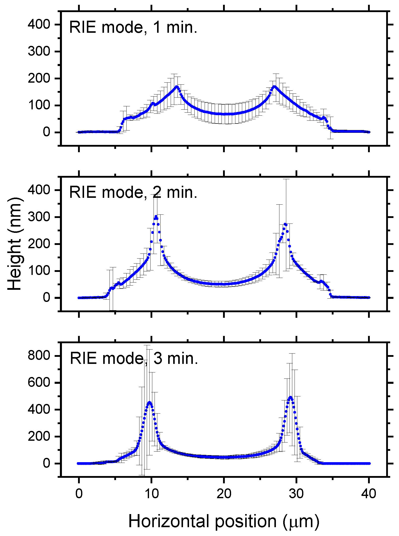
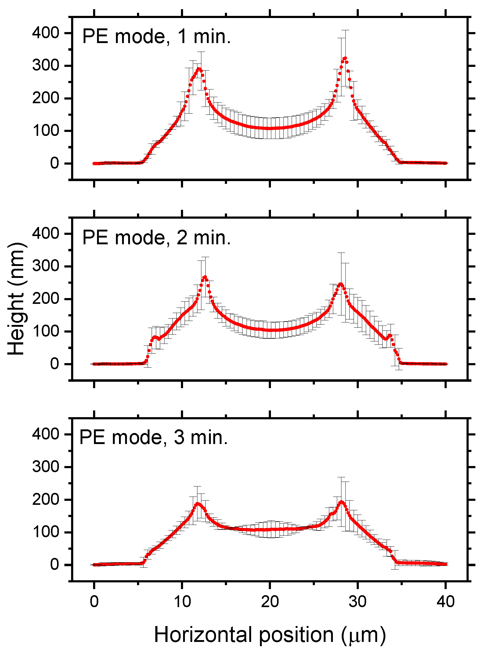
3.4. Adding an O2 Plasma Treatment before Lifting Off the Photoresist

The next step introduces another difficulty that disturbs the uniformity of the patterns. Undesirable patterns, a type of defect, are often observed when lifting off the photoresist. Figure 9 shows an image of typical undesirable patterns remaining on the surface of the patterned PEDOT:PSS, which we assume are related to the PEDOT:PSS covering the top of the photoresist via conformal coverage [30]. Presumably, when the photoresist patterns are lifted off, the PEDOT:PSS anchored to the surface of the photoresist mechanically causes this problem. Further, brush-like wrinkles often appear around the boundaries after spin-coating PEDOT:PSS onto the patterned photoresist, as shown in Figure 10b, which prompts us to consider the effects of conformal coverage. During the spin-coating process, PEDOT:PSS spreads over the entire patterned photoresist surface, meaning that PEDOT:PSS can spread not only in the gaps between the strip patterns but also on top of the patterned lines. Therefore, removing such PEDOT:PSS covering the photoresist before lifting it off would help reduce these defects.
Thus, to remove the PEDOT:PSS from the top of the photoresist caused by conformal coverage, we introduce another O2 plasma process before lifting off the photoresist patterns. As expected, applying this additional O2 plasma treatment at this stage reduces the undesirable patterns and defects in the resulting PEDOT:PSS when the photoresist is finally removed with acetone, as shown in Figure 11. Obviously, however, a longer plasma treatment at this stage also reduces the thickness of PEDOT:PSS itself or even damages the patterns. As an extreme case in which we plasma-treated the PEDOT:PSS pattern for 120 s, its thickness decreased to one-fifth of its designed value, and its linewidths became two-thirds narrower. Further, we observed jagged line patterns, which are side effects of O2 plasma exposure at this stage. Therefore, the operating time of O2 plasma has a trade-off relationship between mitigating these undesirable patterns and maintaining the quality of the PEDOT:PSS patterns.
Nevertheless, adding an O2 plasma treatment at this stage enables the removal of the unfavorable PEDOT:PSS covering the photoresist, suggesting that it is crucial to remove such PEDOT:PSS from the top of the photoresist or avoid conformal coverage. In order to remove this PEDOT:PSS without affecting the film thickness or damaging the film, O2 plasma etching with masking would be more reliable.

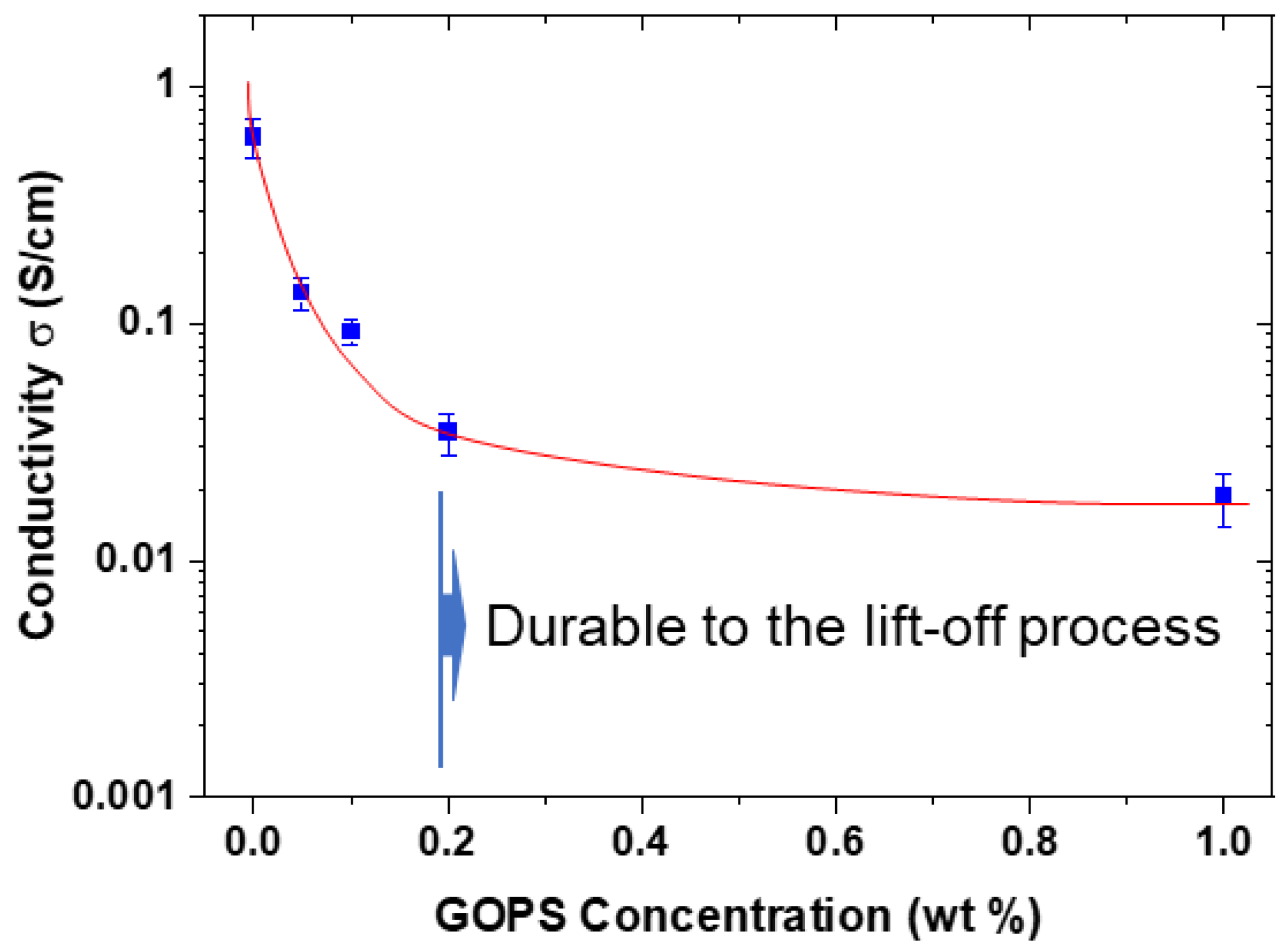
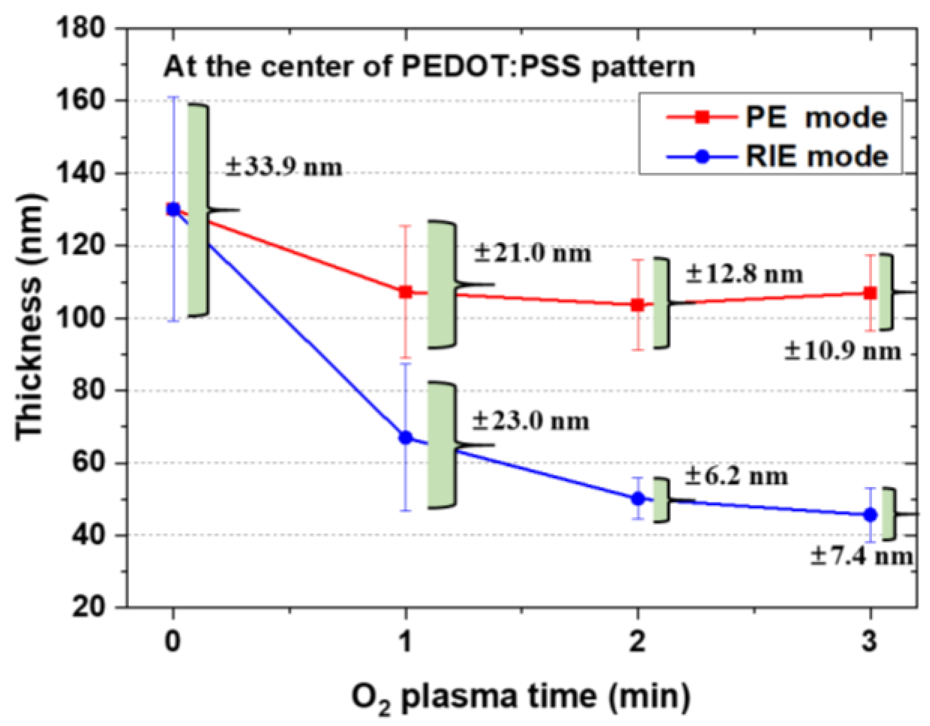
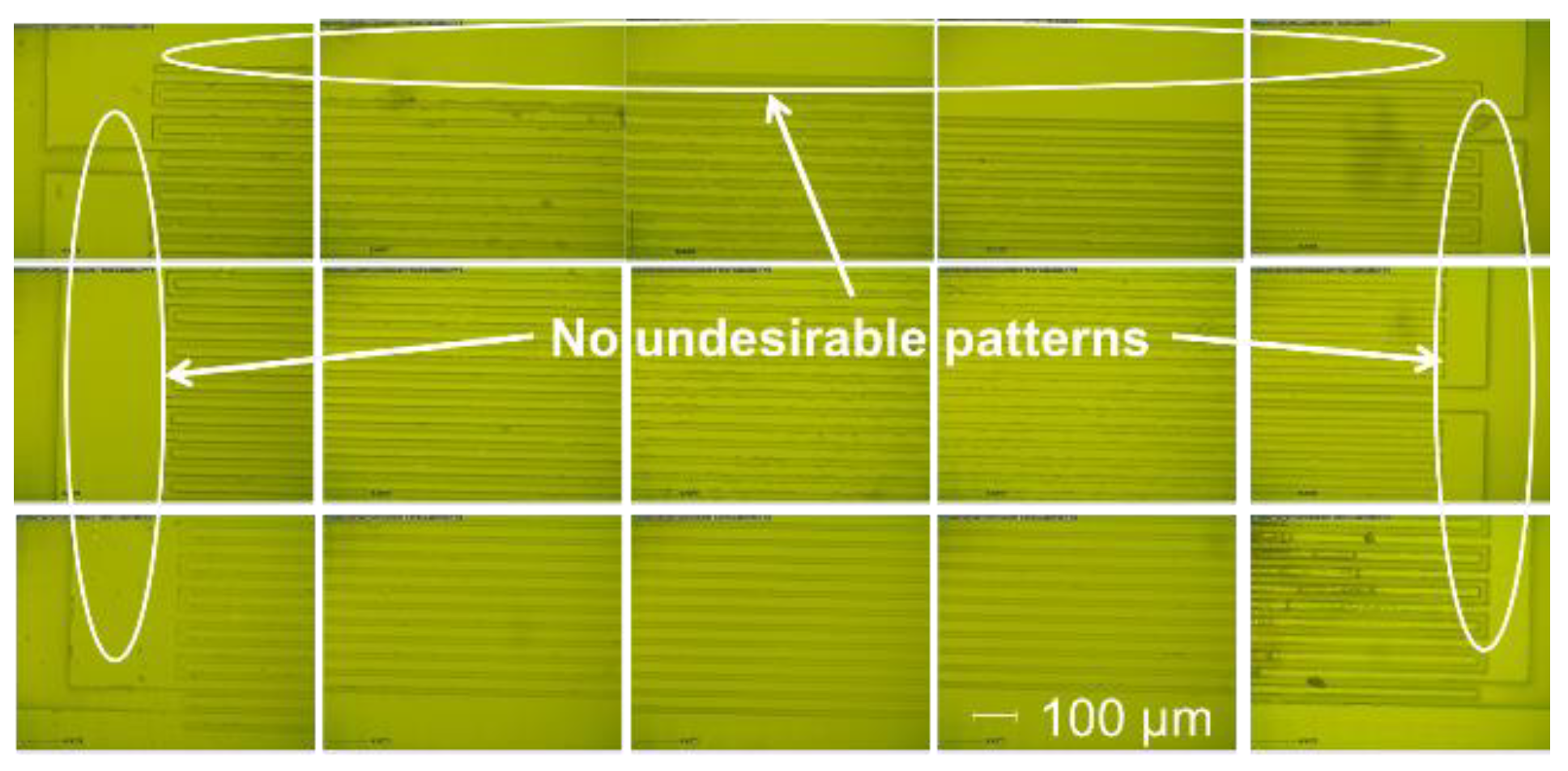
3.5. Combination of the Added O2 Plasma Treatments

Naturally, we are also interested in how combining the two added O2 plasma processes eventually improves the quality of the PEDOT:PSS patterns. We thus optimized the plasma treatment operation time in PE mode to be 3 min before spin-coating PEDOT:PSS and that before lifting off the photoresist in RIE mode to be 1 s. Our investigation reveals that even 1 s of O2 plasma in the RIE mode assists with removing undesirable PEDOT:PSS, thereby promoting the lift-off process while avoiding defects. Figure 12 shows microscopic images and height profiles of the PEDOT:PSS patterns when both O2 plasma treatments are added to the process. Applying both treatments enables fabricating more uniform, defect-free PEDOT:PSS finger-type patterns with a deviation in the thickness of ±10.6 nm at the center of the cross-section. The bottom of the lines is still beyond the designed value, thus requiring further optimization; however, avoiding conformal coverage would be crucial to improving microfabrication using photolithography.

4. Conclusions

We fabricated finger-type PEDOT:PSS electrodes using conventional photolithographic patterning techniques, during which the cross-sectional U-shaped profiles of the PEDOT:PSS patterns were found instead of rectangular cross-sections. The fragility of the PEDOT:PSS patterns was improved by adding 0.2 wt % GOPS to the PEDOT:PSS suspensions. Using the strengthened PEDOT:PSS patterns, we investigated the effects of adding O2 plasma treatments to the traditional photolithography process for patterning PEDOT:PSS, expecting to observe how this treatment improved the uniformity of the patterns and how it changed the thickness and U-shaped profiles of the patterns. One O2 plasma treatment was introduced before spin-coating PEDOT:PSS onto the patterned photoresist layer, and the other was employed before the lift-off process for removing the photoresist layer. The former improved the wettability of the patterned photoresist surface, including that of its sidewalls, and the latter helped partially remove the spin-coated PEDOT:PSS that impeded the lift-off process. In the former O2 plasma treatment, the uniformity of the thickness at the center of the lines became more uniform, with an improved deviation from several tens of nanometers to several nanometers; however, the U-shaped patterns became more pronounced when the sidewalls of the patterned photoresist were exposed to the plasma in RIE mode, which could be avoided using more gentle plasma in PE mode. The latter O2 plasma treatment eventually facilitated the lift-off process while preventing defects, uniformly reducing the entire thickness of the PEDOT:PSS patterns while removing the PEDOT:PSS covering the photoresist. Our findings suggest that the most important factor is how to remove PEDOT:PSS from the top of the photoresist or avoid its conformal coverage. Applying these two additional processes enabled fabricating more uniform, defect-free PEDOT:PSS patterns. Realizing a real THz device using the investigated techniques requires considerable effort to optimize the entire procedure, which would involve many factors, such as the cross-sectional shape of the patterned lines, defects, conductivity, and anchoring strength.

Author Contributions

Conceptualization, C.-L.P. and M.O.; methodology, D.-Y.Z. and M.O.; validation, D.-Y.Z.; formal analysis, D.-Y.Z. and M.O.; investigation, D.-Y.Z. and M.-H.C.; data curation, D.-Y.Z.; writing—original draft preparation, D.-Y.Z.; writing—review and editing, M.O.; visualization, M.O.; supervision, C.-L.P. and M.O.; project administration, C.-L.P. and M.O.; funding acquisition, C.-L.P. and M.O. All authors have read and agreed to the published version of the manuscript.

Funding

This work was supported by grants from the Ministry of Science and Technology (MOST), Taiwan, under Grant MOST 108-2221-E-007-094-MY2 as well as Grants MOST 108-2622-M-007-006-CC1 and 109-2622-M-007-007-CC1 for industrial–academic collaborations jointly funded by MOST and Profound Material Technology Co., Ltd., in Taiwan.

Institutional Review Board Statement

Not applicable.

Informed Consent Statement

Not applicable.

Data Availability Statement

Data sharing not applicable.

Conflicts of Interest

The authors declare no conflict of interest.

References

  1. Zhang, X.-C.; Xu, J. Introduction to THz Wave Photonics; Springer: New York, NY, USA, 2010. [Google Scholar]
  2. Shi, J.-W.; Huang, C.-B.; Pan, C.-L. Millimeter-wave photonic wireless links for very high data rate communication. NPG Asia Mater. 2011, 3, 41–48. [Google Scholar] [CrossRef]
  3. Chen, C.-Y.; Hsieh, C.-F.; Lin, Y.-F.; Pan, R.-P.; Pan, C.-L. Magnetically tunable room-temperature 2π liquid crystal terahertz phase shifter. Opt. Express 2004, 12, 2625–2630. [Google Scholar] [CrossRef]
  4. Wu, H.-Y.; Hsieh, C.-F.; Tang, T.-T.; Pan, R.-P.; Pan, C.-L. Electrically tunable room-temperature 2π liquid crystal terahertz phase shifter. IEEE Photon. Technol. Lett. 2006, 18, 1488–1490. [Google Scholar] [CrossRef]
  5. Lin, X.-W.; Wu, J.-B.; Hu, W.; Zheng, Z.-G.; Wu, Z.-J.; Zhu, G.; Xu, F.; Jin, B.-B.; Lu, Y.-Q. Self-polarizing terahertz liquid crystal phase shifter. AIP Adv. 2011, 1, 032133. [Google Scholar] [CrossRef] [Green Version]
  6. Yang, C.-S.; Tang, T.-T.; Chen, P.-H.; Pan, R.-P.; Yu, P.; Pan, C.-L. Voltage-controlled liquid-crystal terahertz phase shifter with indium–tin–oxide nanowhiskers as transparent electrodes. Opt. Lett. 2014, 39, 2511. [Google Scholar] [CrossRef] [PubMed]
  7. Yang, C.-S.; Tang, T.-T.; Pan, R.-P.; Yu, P.; Pan, C.-L. Liquid crystal terahertz phase shifters with functional indium-tin-oxide nanostructures for biasing and alignment. Appl. Phys. Lett. 2014, 104, 141106. [Google Scholar] [CrossRef] [Green Version]
  8. Yang, C.-S.; Kuo, C.; Chen, P.-H.; Wu, W.-T.; Pan, R.-P.; Yu, P.; Pan, C.-L. High-transmittance 2π electrically tunable terahertz phase shifter with CMOS-compatible driving voltage enabled by liquid crystals. Appl. Sci. 2019, 9, 271. [Google Scholar] [CrossRef]
  9. Chiang, Y.-J.; Yang, C.-S.; Yang, Y.-H.; Pan, C.-L.; Yen, T.-J. An ultrabroad terahertz bandpass filter based on multiple-resonance excitation of a composite metamaterial. Appl. Phys. Lett. 2011, 99, 191909. [Google Scholar] [CrossRef] [Green Version]
  10. Chatzakis, I.; Tassin, P.; Luo, L.; Shen, N.-H.; Zhang, L.; Wang, J.; Koschny, T.; Soukoulis, C.M. One- and two-dimensional photo-imprinted diffraction gratings for manipulating terahertz waves. Appl. Phys. Lett. 2013, 103, 043101. [Google Scholar] [CrossRef] [Green Version]
  11. Hsieh, C.-F.; Lai, Y.-C.; Pan, R.-P.; Pan, C.-L. Polarizing terahertz waves with nematic liquid crystals. Opt. Lett. 2008, 33, 1174. [Google Scholar] [CrossRef] [Green Version]
  12. Sahoo, A.K.; Yang, C.-S.; Wada, O.; Pan, C.-L. Twisted nematic liquid crystal based terahertz phase shifter with crossed indium tin oxide finger type electrodes. IEEE Trans. Terahertz Sci. Technol. 2019, 9, 399–408. [Google Scholar] [CrossRef]
  13. Yang, C.-S.; Kuo, C.; Tang, C.-C.; Chen, J.C.; Pan, R.-P.; Pan, C.-L. Liquid-crystal terahertz quarter-wave plate using chemical-vapor-deposited graphene electrodes. IEEE Photon. J. 2015, 7, 2200808. [Google Scholar] [CrossRef]
  14. Kim, N.; Kee, S.; Lee, S.H.; Lee, B.H.; Kahng, Y.H.; Jo, Y.-R.; Kim, B.-J.; Lee, K. Highly conductive PEDOT:PSS nanofibrils induced by solution-processed crystallization. Adv. Mater. 2014, 26, 2268–2272. [Google Scholar] [CrossRef]
  15. Sun, K.; Zhang, S.; Li, P.; Xia, Y.; Zhang, X.; Du, D.; Isikgor, F.H.; Ouyang, J. Review on application of PEDOTs and PEDOT:PSS in energy conversion and storage devices. J. Mater. Sci. Mater. Electron. 2015, 26, 4438–4462. [Google Scholar] [CrossRef]
  16. Ouyang, S.; Xie, Y.; Wang, D.; Zhu, D.; Xu, X.; Tan, T.; Fong, H.H. Surface patterning of PEDOT:PSS by photolithography for organic electronic devices. J. Nanomater. 2015, 2015, 603148. [Google Scholar] [CrossRef] [Green Version]
  17. Sun, Y.; Yang, S.; Du, P.; Yan, F.; Qu, J.; Zhu, Z.; Zuo, J.; Zhang, C. Investigate the effects of EG doping PEDOT/PSS on transmission and anti-reflection properties using terahertz pulsed spectroscopy. Opt. Express 2017, 25, 1723. [Google Scholar] [CrossRef] [PubMed]
  18. Rwei, S.-P.; Lee, Y.-H.; Shiu, J.-W.; Sasikumar, R.; Shyr, U.-T. Characterization of solvent-treated PEDOT:PSS thin films with enhanced conductivities. Polymers 2019, 11, 134. [Google Scholar] [CrossRef] [Green Version]
  19. Huseynova, G.; Hyun Kim, Y.; Lee, J.-H.; Lee, J. Rising advancements in the application of PEDOT:PSS as a prosperous transparent and flexible electrode material for solution-processed organic electronics. J. Inf. Disp. 2020, 21, 71–91. [Google Scholar] [CrossRef] [Green Version]
  20. Ling, H.; Liu, S.; Zheng, Z.; Yan, F. Organic flexible electronics. Small Methods 2018, 2, 1800070. [Google Scholar] [CrossRef]
  21. Fan, X.; Nie, W.; Tsai, H.; Wang, N.; Huang, H.; Cheng, Y.; Wen, R.; Ma, L.; Yan, F.; Xia, Y. PEDOT:PSS for flexible and stretchable electronics: Modifications, strategies, and applications. Adv. Sci. 2019, 6, 1900813. [Google Scholar] [CrossRef] [Green Version]
  22. Hwang, H.S.; Zakhidov, A.A.; Lee, J.-K.; André, X.; Defranco, J.A.; Fong, H.H.; Holmes, A.B.; Malliaras, G.G.; Ober, C.K. Dry photolithographic patterning process for organic electronic devices using supercritical carbon dioxide as a solvent. J. Mater. Chem. 2008, 18, 3087–3090. [Google Scholar] [CrossRef]
  23. Lee, J.-K.; Taylor, P.G.; Zakhidov, A.A.; Fong, H.H.; Hwang, H.S.; Chatzichristidi, M.; Malliaras, G.G.; Ober, C.K. Orthogonal processing: A novel photolithographic patterning method for organic electronics. J. Photopolym. Sci. Technol. 2009, 22, 565–569. [Google Scholar] [CrossRef] [Green Version]
  24. Khong, S.-H.; Sivaramakrishnan, S.; Png, R.-Q.; Wong, L.-Y.; Chia, P.-J.; Chua, L.-L.; Ho, P.K.H. General photo-patterning of polyelectrolyte thin films via efficient ionic bis(fluorinated phenyl azide) photo-crosslinkers and their post-deposition modification. Adv. Funct. Mater. 2007, 17, 2490–2499. [Google Scholar] [CrossRef]
  25. Winroth, G.; Latini, G.; Credgington, D.; Wong, L.-Y.; Chua, L.-L.; Ho, P.K.-H.; Cacialli, F. Polyfluorene-based light-emitting diodes with an azide photocross-linked poly(3,4-ethylene dioxythiophene):(polystyrene sulfonic acid) hole-injecting layer. Appl. Phys. Lett. 2008, 92, 103308. [Google Scholar] [CrossRef]
  26. Fenwick, O.; Oliver, K.; Cacialli, F. Cross-linking of a poly(3,4-ethylene dioxythiophene):(polystyrene sulfonic acid) hole injection layer with a bis-azide salt and the effect of atmospheric processing conditions on device properties. Appl. Phys. Lett. 2012, 100, 053309. [Google Scholar] [CrossRef]
  27. Yoshida, S.; Hagiwara, K.; Hasebe, T.; Hotta, A. Surface modification of polymers by plasma treatments for the enhancement of biocompatibility and controlled drug release. Surf. Coatings Technol. 2013, 233, 99–107. [Google Scholar] [CrossRef]
  28. Håkansson, A.; Han, S.; Wang, S.; Lu, J.; Braun, S.; Fahlman, M.; Berggren, M.; Crispin, X.; Fabiano, S. Effect of (3-glycidyloxypropyl)trimethoxysilane (GOPS) on the electrical properties of PEDOT:PSS films. J. Polym. Sci. Part B Polym. Phys. 2017, 55, 814–820. [Google Scholar] [CrossRef] [Green Version]
  29. He, J.; Wan, Y.; Gao, P.; Tang, J.; Ye, J. Over 16.7% efficiency organic-silicon heterojunction solar cells with solution-processed dopant-free contacts for both polarities. Adv. Funct. Mater. 2018, 28, 1802192. [Google Scholar] [CrossRef]
  30. Chan, J.R.; Huang, X.Q.; Song, A.M. Nondestructive photolithography of conducting polymer structures. J. Appl. Phys. 2006, 99, 023710. [Google Scholar] [CrossRef] [Green Version]
  31. Athreya, S.; Venkatesh, Y.D. Application of Taguchi method for optimization of process parameters in improving the surface roughness of lathe facing operation. Int. Ref. J. Eng. Sci. 2012, 1, 13–19. [Google Scholar]
  32. Yoon, S.-S.; Khang, D.-Y. Roles of nonionic surfactant additives in PEDOT:PSS thin films. J. Phys. Chem. C 2016, 120, 29525–29532. [Google Scholar] [CrossRef]
  33. Wang, X.; Östblom, M.; Johansson, T.; Inganäs, O. PEDOT surface energy pattern controls fluorescent polymer deposition by dewetting. Thin Solid Films 2004, 449, 125–132. [Google Scholar] [CrossRef]
  34. Charlot, B.; Sassine, G.; Garraud, A.; Sorli, B.; Giani, A.; Combette, P. Micropatterning PEDOT:PSS layers. Microsyst. Technol. 2013, 19, 895–903. [Google Scholar] [CrossRef]
  35. Deegan, R.D.; Bakajin, O.; Dupont, T.F.; Huber, G.; Nagel, S.R.; Witten, T.A. Capillary flow as the cause of ring stains from dried liquid drops. Nature 1997, 389, 827–829. [Google Scholar] [CrossRef]
  36. Deegan, R.D.; Bakajin, O.; Dupont, T.F.; Huber, G.; Nagel, S.R.; Witten, T.A. Contact line deposits in an evaporating drop. Phys. Rev. E Stat. Phys. Plasmas Fluids Relat. Interdiscip. Top. 2000, 62, 756–765. [Google Scholar] [CrossRef] [PubMed] [Green Version]
Figure 1. Designed mask pattern for a unit cell (right) and enlargement of the finger-type electrodes (left).
Coatings 11 00031 g001
Figure 2. Poly (3,4-ethylenedioxythiophene) polystyrene sulfonate (PEDOT:PSS) film damaged when the substrate was shaken in an acetone bath during the lift-off process. (a) Image of the finger-type electrodes observed using an optical microscope. (b) Macroscale image of the entire substrate.
Coatings 11 00031 g002
Figure 3. Changes in conductivity of PEDOT:PSS films when (3-glycidyloxypropyl)trimethoxysilane (GOPS) is added to PEDOT:PSS suspensions. The solid curve is a visual guide.
Coatings 11 00031 g003
Figure 4. Height profiles of the patterned PEDOT:PSS lines made using the traditional process. The error bars show the difference in the maximum and minimum values at each position.
Coatings 11 00031 g004
Figure 5. Effects of exposing O2 plasma to the surface of the patterned photoresist on its wettability.
Coatings 11 00031 g005
Figure 6. Height profiles of the patterned PEDOT:PSS lines made by plasma-treating the photoresist in reactive-ion etching (RIE) mode before spin-coating PEDOT:PSS. The error bars show the maximum and minimum values at each position.
Coatings 11 00031 g006
Figure 7. Height profiles of the patterned PEDOT:PSS lines made by plasma-treating the photoresist in plasma etching (PE) mode before spin-coating PEDOT:PSS. The error bars show the maximum and minimum values at each position.
Coatings 11 00031 g007
Figure 8. Changes in thickness and its variability at the center of the PEDOT:PSS patterns as a function of O2 plasma exposure time using PE and RIE modes.
Coatings 11 00031 g008
Figure 9. Typical undesirable patterns remaining on the surface of the patterned PEDOT:PSS observed using an optical microscope.
Coatings 11 00031 g009
Figure 10. Photoresist patterns (a) before and (b) after spin-coating PEDOT:PSS observed using an optical microscope.
Coatings 11 00031 g010
Figure 11. Microscopic image of undesirable patterns being removed when adding O2 plasma in RIE mode for 15 s.
Coatings 11 00031 g011
Figure 12. (a) Microscopic images and (b) height profiles of the PEDOT:PSS patterns made by adding both O2 plasma treatments to traditional photolithography.
Coatings 11 00031 g012
Publisher’s Note: MDPI stays neutral with regard to jurisdictional claims in published maps and institutional affiliations.

