Abstract
Metallic nanoparticle ensemble, with narrow inter-particle distance, is a useful element for diverse optical devices due to highly enhanced electric field intensity at the gap. Self-assembly of block copolymer (BCP) can provide the versatile solution to fabricate precise nanostructures, but this methodology has the intrinsic limitation to realize optically coupled metallic multimer geometry with narrow inter-particle distance. This is because BCP-based nanotemplate possesses a minimum size limit for interparticle distance imposed by its thermodynamic restriction. Herein, we investigate the facile formation of metallic multimer with scalability and area-selectivity through the collapse of self-assembled BCP nanopattern. The capillary-force-induced collapse phenomenon enables a spatial transformation of lateral regular ordering in metallic nanoparticle array and enhances electric field intensity. The fabrication of this metallic nanoparticle ensemble from BCP lithography is successfully utilized for surface enhanced Raman scattering (SERS). The enhancement factor of metal nanoparticle multimer is calculated as ~6.74 × 10⁵ at 1000 cm−1, 2.04 × 10⁶ at 1022 cm−1, and 6.11 × 10⁶ at 1580 cm−1, respectively.
1. Introduction
Localized surface plasmon resonance (LSPR), the collective motion of conduction electrons in metallic nanoparticles excited by light, has been exploited mainly due to its novel electric near-field enhancement at the resonance frequency [1,2,3,4]. Many functional devices can take the advantages of this strong electric field, such as the facile exciton generation and dissociation in a photovoltaic cell [5,6], and signal amplification in photonic devices [7,8]. It is highly important that effective design and facile fabrication of metallic nanostructures with ultra-intense electric near-field for these purposes. Among several effective nanostructures, metallic nanoparticles coupled with extremely small gaps can generate a much stronger near-field profile at the gap region compared to single metallic nanoparticle configurations. This lets further performance improvement in optoelectronic applications [9].
Block copolymer (BCP) can provide the uniform and periodic nanotemplate with scalability at a low cost [10,11]. Pattern transfer methodologies of BCP such as ion immersion, spin coating of precursor, conventional evaporation/lift-off process, and atomic layer deposition (ALD) enable fabrication of the metallic nanostructure following the morphology of organic nanotemplate [12]. However, due to the intrinsic thermodynamic nature of self-assembly, BCP forms the nanostructures with relatively large inter-particle distance. The fabricated nanostructures with large inter-particle distance lead pattern transfer into the monomeric metallic nanoparticle array with weak optical coupling. Therefore, for the active utilization of BCP self-assembly in LSPR, the pattern dimension of BCP should be manipulated to induce the strong optical coupling between metallic nanoparticles [13,14].
In this work, we introduce the novel metallic nanoparticle array with an extremely small gap by using the BCP nanotemplate and capillary-force-induced collapse phenomenon. In general, a nanopattern collapse is regarded as the critical failure during the micro/nanostructure fabrication processes, induced by bending, peeling, and breaking of narrow patterns. This phenomenon, however, was often induced with intention as an unusual fabrication process [15,16,17,18]. Herein, we actively utilize nanopattern collapse for regulating the inter-particle distance of metallic nanoparticle array fabricated from BCP lithography. The spatial clustering of high-aspect-ratio (about 2~3) nanostructures by capillary force during the liquid drying enables the dramatic reduction of inter-particle distances between self-assembled metallic nanoparticles (<10 nm) [19]. By the favor of this strong optical coupling, surface enhanced Raman scattering (SERS) for organic molecules could be successfully demonstrated with an enhancement factor of ~106 [20,21,22]. The remarkable advantage of this approach is uniformity over a large area and area-selectivity. Although the local ordering of nanoparticle array at multimer configuration is lost by pattern collapse, microscopic pattern uniformity can still maintain, which leads to SERS uniformity.
2. Materials and Methods
The collapse phenomenon easily occurs at nanopattern array with high-aspect-ratio and small pitch, due to increased capillary force. To promote such nanostructure, we develop a novel fabrication process for the self-assembled, periodic metallic nanoparticle array on an easily removable polymeric substrate. In this case, a simple dry etching process can generate the high-aspect-ratio polymeric pillar array due to high etching contrast with metallic nanoparticle and polymer substrate. The fabrication of self-assembled multimer is a two-step process; (i) the transfer of metallic nanoparticle array onto the polymeric substrate and (ii) pattern collapse after polymeric pillar array formation. The conventional BCP lithography is hardly achieved on the easily disposable polymeric substrate due to its low thermal and chemical stability. Therefore, the transfer of metallic nanoparticle array mediating chemically modified graphene (CMG) layer, which is a universal transfer layer regardless of substrate types, is used. We utilize CMG as a robust and compliant transferrable layer of self-assembled nanopattern using procedures similar to those described previously [23,24,25,26].
2.1. Block Copolymer Self-Assembly Process on Chemically Modified Graphene Layer
Figure 1a shows the conventional fabrication process for metal nanoparticle array on a silicon wafer using BCP lithography. The fabricated metal nanoparticle array has an intrinsically large gap size (~62 nm), thereby leading to weak optical coupling. Figure 1b shows the detailed schematic illustration for the formation of the self-assembled multimer by nanopattern collapse. All materials were used without further purification. First, the graphene oxide (Sigma-Aldrich, St. Louis, MO, USA) solution with a concentration of ~1 wt% was made by the modified Hummers method. The prepared graphene oxide solution was spin coated on the silicon oxide (500 nm)/Si substrate. A polystyrene-block-poly (methylmethacrylate) (PS-b-PMMA) with a molecular weight of 140 kg/mol-b-65 kg/mol (Polymer Source INC., Montreal, QC, Canada) was used for the fabrication of a self-assembled template. In order for BCP to have the substrate-perpendicular orientation, surface energy of the spin-cast graphene oxide layer (thickness ~15 nm) was modified using a thermal treatment over 600 °C. Afterward, PS-b-PMMA BCP thin film (thickness ~90 nm) was formed and self-assembled on the CMG layer through thermal annealing at 250 °C. After partial crosslinking of PS block of PS-b-PMMA using UV irradiation, PMMA block was etched out by Ar/O2 plasma. Finally, Au nanoparticle (thickness ~15 nm) array replicating the self-assembled template was formed through the thermal evaporation and lift-off process.
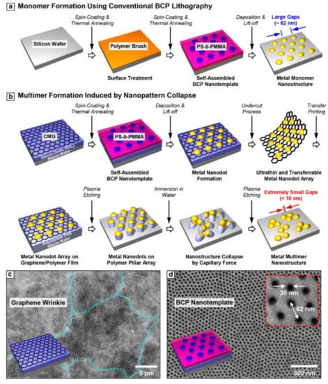
Figure 1.
The schematic illustration of metal (a) monomer and (b) multimer fabrication process by conventional BCP lithography and capillary force induced nanopattern collapse, respectively. The top view SEM images of (c) chemically modified graphene (CMG) and the substrate-perpendicular (d) BCP nanotemplate.
2.2. Formation of the Gold Nanoparticle Multimer
The Au nanoparticle array on the CMG layer was floated on the diluted hydrogen fluoride (HF, 5 wt %) solution after etching out the silicon dioxide (SiO2) layer. Then, the floating layer was transferred on the DI water to remove the HF trace and then transferred to UVO treated polystyrene (PS) thin film with a thickness of ~200 nm. Afterward, the PS was etched using the Au nanoparticle array. Because of the high etching contrast between metal and polymer thin film, the high-aspect-ratio (about 2~3) PS pillar was formed by oxygen reactive ion etching (O2 RIE; experimental condition). Afterward, the PS pillar structure was immersed in the water, a poor solvent for the polymer, and dried subsequently to form a collapsed pillar configuration [27]. Finally, the collapsed PS pillar was completely removed by an additional dry etching process (O2 RIE; experimental condition) to form a pure metallic nanoparticle multimer without organic contamination. It should be noted here that CMG used as a transfer layer can be easily removed during the plasma treatment because it consists of carbon and oxygen. The successfully fabricated metal nanoparticle multimer has a <10 nm gap size on average. Figure 1c,d show the top-view scanning electron microscope (SEM) images of the CMG layer and BCP nanotemplate used for this experiment, respectively.
2.3. Characterization
For the optical property measurement, commercially available ultra-violet-vis spectroscopy (UV-2600, SIMIADZU, Kyoto, Japan) was used. For a probe molecule, benzenethiol (BT, Sigma-Aldrich) was utilized owing to its well-known optical response. To monitor the Raman signal enhancement, commercially available Raman spectroscopy (ARAMIS, Horiba Jobin Yvon, Edison, NJ, USA) was used. The diluted BT solution was dropped on the monomer and multimer substrate and enough time for BT to chemically react to the Au surface was allowed. After that, the non-bonded BT molecules were washed out. The morphology of the sample was observed using an optical microscope (Carl Zeiss, Oberkochen, Germany, SN 449) and a field emission scanning electron microscope (Hitachi, Chiyoda City, Tokyo, Japan, S-4700) with an acceleration voltage of 5 kV.
3. Results and Discussion
Figure 2a,b show the SEM images of Au nanoparticles conjugated PS pillar array before and after the pattern collapse process, respectively. In Figure 2a, most metal nanoparticles have a large inter-particle distance (~62 nm) compared with their diameter (~30 nm), maintaining the intrinsic morphology of BCP nanotemplate. On the other hand, after the water immersion and subsequent drying process, Au nanoparticle conjugated PS pillars were completely collapsed by strong capillary force. Among the various collapse mechanisms, collapse in our system occurred by bending of PS pillar due to its flexibility (Figure 2b). With the collapse event, we found the dramatic decrease of the inter-particle distance of Au nanoparticle array into a nearly touchable scale. This collapse-induced inter-particle distance shrinkage was successfully realized for PS pillar in a wide range of aspect ratios (2~3). The percentage of multimer per unit area was confirmed by ~58%, which means that the ~76% of single nanoparticles per unit area before collapse contributes to multimer formation (Figure 2c). This successful transformation of inter-particle distance shrinkage is detectable with a naked eye by a color change from red (monomer) to blue (multimer) (Figure 2d).
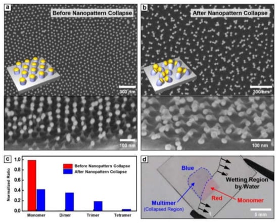
Figure 2.
The top and tilted view SEM images of Au nanoparticles on PS pillar (a) before and (b) after nanopattern collapse. (c) The number percentage of Au monomer, dimer, trimer, and tetramer after nanopattern collapse. (d) The photographic image of metal monomer and multimer during the drying process.
The change of optical color is based on the plasmonic resonance of metallic nanoparticles depending on the inter-particle distance. To investigate these optical properties, the transmittance of Au nanoparticle array before and after nanopattern collapse was measured by UV-vis spectroscopy (Figure 3a). Au nanoparticle array before nanopattern collapse showed the lowest transmittance at ~545 nm, which is commonly observed resonant behavior of collective electron motion in the Au nanoparticle system. On the other hand, after the nanopattern collapse, the resonance absorption at 545 nm was significantly diminished and a broad dip at 650 nm was observed. While a small dip at 545 nm is regarded as the remaining of monomeric Au nanoparticles and off-axis resonance with adjacent nanoparticles, the newly appearing dip at 650 nm is attributed to the formation of Au nanoparticle multimer with an extremely small gap.
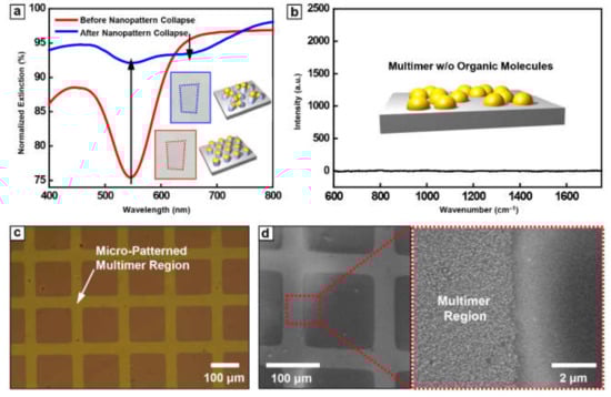
Figure 3.
The characterization of Au arrays and micropattern feasibility. (a) UV-Vis spectroscopy graph of Au nanoparticles on PS pillar before (red line) and after (blue line) immersion in DI water. (b) The Raman spectra of Au multimer after PS pillar removal. The (c) optical microscope and (d) SEM images of micro-patterned Au multimer array fabricated through conventional photolithography and wet etching process.
In contrast with relatively weak electric field intensity around metallic monomer, strong electric field intensity within an extremely small gap of metallic multimer can be utilized for various functional optoelectronic devices such as solar cell [28,29,30], light emitting devices [31], and bio-sensors [32,33]. One of the important strategies for enhancing such devices’ performance is utilizing the SERS phenomenon, which also takes benefits of a strong electric field. To test whether metallic multimer can be utilized for SERS in the detection of organic molecules, we studied the presence of possible organic contamination, a basic requirement for the detection of various target organic molecules.
Figure 3b presents the Raman spectroscopy data for Au nanoparticle multimer without any loading of an organic molecule to investigate a complete removal of organic residues. There was no noticeable peak measured for the wide wavenumber range of 600 cm−1 to 1800 cm−1 (Figure 3b). From these results, we confirm the residue-free surface after multimer formation, emphasizing the utility of our approach for the detection of organic molecules. Another merit of this method is area-selectivity for the formation of the multimer. Basically, BCP lithography is compatible with various top-down lithography such as conventional photo- and soft- lithography. Therefore, the area-selective formation of Au nanoparticle multimer could be easily realized. Figure 3c,d show optical microscope and SEM images of multimer array, patterned by conventional photolithography and wet etching. The compatibility of metal multimer fabrication with the conventional microfabrication process indicates that one can easily utilize our methodology in the development of various optoelectronic/electronic devices.
Here, the SERS effect of Au nanoparticle multimer was evaluated using probe molecule, benzenethiol (BT), owing to its well-established vibration properties [34,35]. The loading process of BT, utilizing the thiol group of BT to conjugate with surface Au atoms, was performed through immersion of Au nanoparticle multimer in BT aqueous solution for several hours. Afterward, Au nanoparticle multimer washed with water several times and dried to remove the unbonded BT molecules [36]. For the control experimental, an identical loading process was carried out for the Au nanoparticle monomer with a relatively large inter-particle distance. Figure 4a shows top-view SEM images of BT-conjugated Au nanoparticle monomer (top image) and multimer (bottom image) used in Raman experiments. In Figure 4b, the highly increased Raman signal was measured in the case of Au nanoparticle multimer (blue line) compared with the Au nanoparticle monomer (red line), which apparently indicates that a decrease of inter-particle distance between Au nanoparticles generates strong electric near-field, leading Raman signal enhancement. To calculate the SERS enhancement factor of Au nanoparticle multimer, the pure BT as a reference and the number of BT molecules in the laser focal volume of Raman spectroscopy was measured and calculated, respectively (Figure S1) [37]. Also, considering number density of BT molecule at the Au surface (~6.8 nm−2) and the dimensions of ellipsoid-assumed nanoparticle (diameter of 30 nm and height of 10 nm), the BT molecules bonded to Au nanoparticles within laser spot was evaluated. From these values, the enhancement factor of Au nanoparticle multimer is calculated as ~6.74 × 10⁵ at 1000 cm−1, 2.04 × 10⁶ at 1022 cm−1, and 6.11 × 10⁶ at 1580 cm−1, respectively.
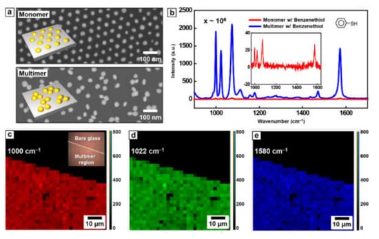
Figure 4.
(a) The top-view SEM images of Au nanoparticle monomer (top) and multimer (bottom) without PS pillars. (b) Raman spectra of Au monomer and multimer array conjugated with benzenethiol (BT) molecules. Raman signals from 900 spots on 140 μm × 140 μm glass at (c) 1000 cm−1, (d) 1022 cm−1, and (e) 1580 cm−1, respectively.
One remarkable advantage of this BCP-based approach for the formation of the multimeric nanostructure is uniformity over a large area. This collapse-induced method only utilizes the local distortion of lateral ordering for controlling the period of Au nanoparticle array. Thus, pattern uniformity over a large area originated from BCP lithography methodology is still maintained. Accordingly, the uniformity of SERS can be secured over a large area as it can be easily seen from the measured Raman signals from 900 spots on 140 μm × 140 μm glass (Figure 4c–e). Referring inset optical image of Figure 4c, only the region with Au nanoparticle multimer (left low part) shows the uniform and strong signal enhancement, revealing the high reproducibility.
4. Conclusions
In summary, we have demonstrated the collapse-induced metal multimer formation of self-assembled nanoparticles, a configuration generating strong electric near-field. The formation of metallic nanoparticle on disposable polymeric substrate enabled to fabricate collapsible pillar structure with a wide range of high-aspect-ratio nanostructures. Such nanostructure was easily collapsed by liquid drop and subsequent drying, forming the optically coupled multimer. The strong interaction between metallic nanoparticles could be utilized for the SERS for sensing applications, which shows the ~106 enhancement factor. Because this simple approach can be realized with spatial controllability, other novel applications such as photovoltaic, photodetector, light emitting, refractive index tuning, photocatalyst and so on, would take merits of this methodology.
Supplementary Materials
The following are available online at https://www.mdpi.com/2079-6412/11/1/76/s1.
Author Contributions
Investigation, Y.T.O., S.E.L., J.H.P., S.P., Y.C.K., J.P.H., S.W.S., T.S.Y., S.H.K., S.G.L., and M.K.J.; Supervision, J.Y.K. and B.H.K.; Writing—review & editing, J.Y.K. and B.H.K. All authors have read and agreed to the published version of the manuscript.
Funding
This research was supported by (1) The National Research Foundation of Korea (NRF) grant funded by the Korea government (MSIT) (No. 2020R1C1C1014980), (2) Creative Materials Discovery Program through the National Research Foundation of Korea (NRF) funded by Ministry of Science and ICT (NRF-2018M3D1A1058972), (3) Nanomaterial Technology Development Program (NRF-2016M3A7B4905613) through the National Research Foundation of Korea (NRF) funded by the Ministry of Science, ICT and Future Planning, and (4) Korea Institute for Advancement of Technology (KIAT) grant funded by the Korea Government (MOTIE) (P0012770).
Data Availability Statement
No new data were created or analyzed in this study. Data sharing is not applicable to this article.
Conflicts of Interest
The authors declare no conflict of interest.
References
- Agrawal, A.; Cho, S.H.; Zandi, O.; Ghosh, S.; Johns, R.W.; Milliron, D.J. Localized Surface Plasmon Resonance in Semiconductor Nanocrystals. Chem. Rev. 2018, 118, 3121–3207. [Google Scholar] [CrossRef] [PubMed]
- Bohren, C.F.; Huffman, D.R. Absorption and Scattering of Light by Small Particles; John Wiley & Sons: Hoboken, NJ, USA, 1998; pp. 287–324. [Google Scholar]
- Willets, K.A.; van Duyne, R.P. Localized surface plasmon resonance spectroscopy and sensing. Annu. Rev. Phys. Chem. 2007, 58, 267–297. [Google Scholar] [CrossRef] [PubMed]
- Zhu, S.; Fan, C.; Wang, J.; He, J.; Liang, E. Self-Assembled Ag Nanoparticles for Surface Enhanced Raman Scattering. Opt. Rev. 2013, 20, 361–366. [Google Scholar] [CrossRef]
- Moon, K.S.; Choi, E.J.; Bae, J.M.; Park, Y.B.; Oh, S. Visible light-enhanced antibacterial and osteogenic functionality of Au and Pt nanoparticles deposited on TiO2 nanotubes. Materials 2020, 13, 3721. [Google Scholar] [CrossRef] [PubMed]
- Kumar, P.; Fiaboe, K.F.; Roy, J.S. Design of nonlinear photonic crystal fibers with ultra-flattened zero dispersion for supercontinuum generation. ETRI J. 2020, 42, 282–291. [Google Scholar] [CrossRef]
- Jain, P.K.; Huang, X.; El-Sayed, I.H.; El-Sayed, M.A. Noble metals on the nanoscale: Optical and photothermal properties and some applications in imaging, sensing, biology, and medicine. Acc. Chem. Res. 2008, 41, 1578–1586. [Google Scholar] [CrossRef]
- Zhou, J.; Yang, T.; Chen, J.; Wang, C.; Zhang, H.; Shao, Y. Two-dimensional nanomaterial-based plasmonic sensing applications: Advances and challenges. Coord. Chem. Rev. 2020, 410, 213218. [Google Scholar] [CrossRef]
- Kaminska, I.; Maurer, T.; Nicolas, R.; Renault, M.; Lerond, T.; Salas-Montiel, R.; Herro, Z.; Kazan, M.; Niedziolka-Jönsson, J.; Plain, J.; et al. Near-field and far-field sensitivities of LSPR sensors. J. Phys. Chem. C 2015, 119, 9470–9476. [Google Scholar] [CrossRef]
- Kim, S.O.; Solak, H.; Stoykovich, M.; Ferrier, N.J.; de Pablo, J.J.; Nealey, P.F. Epitaxial self-assembly of block copolymers on lithographically defined nanopatterned substrates. Nature 2003, 424, 411–414. [Google Scholar] [CrossRef]
- Park, M.; Harrison, C.; Chaikin, P.M.; Register, R.A.; Adamson, D.H. Block copolymer lithography: Periodic arrays of ~1011 holes in 1 square centimeter. Science 1997, 276, 1401–1404. [Google Scholar] [CrossRef]
- Warren, S.C.; Messina, L.C.; Slaughter, L.S.; Kamperman, M.; Zhou, Q.; Gruner, S.M.; DiSalvo, F.J.; Wiesner, U. Ordered mesoporous materials from metal nanoparticle-block copolymer self-assembly. Science 2008, 320, 1748–1752. [Google Scholar] [CrossRef] [PubMed]
- Wang, Y.; Becker, M.; Wang, L.; Liu, J.; Scholz, R.; Peng, J.; Gösele, U.; Christiansen, S.; Kim, D.H.; Steinhart, M. Nanostructured gold films for SERS by block copolymer-templated galvanic displacement reactions. Nano Lett. 2009, 9, 2384–2389. [Google Scholar] [CrossRef] [PubMed]
- Jin, H.M.; Kim, J.Y.; Heo, M.; Jeong, S.J.; Kim, B.H.; Cha, S.K.; Han, K.H.; Kim, J.H.; Yang, G.G.; Shin, J.; et al. Ultralarge Area Sub-10 nm Plasmonic Nanogap Array by Block Copolymer Self-Assembly for Reliable High-Sensitivity SERS. ACS Appl. Mater. Interfaces 2018, 10, 44660–44667. [Google Scholar] [CrossRef] [PubMed]
- Chini, S.F.; Amirfazli, A. Understanding pattern collapse in photolithography process due to capillary forces. Langmuir 2010, 26, 13707–13714. [Google Scholar] [CrossRef] [PubMed]
- Ouakad, H.M.; Younis, M.I. Modeling and simulations of collapse instabilities of microbeams due to capillary forces. Math. Probl. Eng. 2009, 2009, 871902. [Google Scholar] [CrossRef]
- Lee, H.J.; Park, J.T.; Yoo, J.Y.; An, I.; Oh, H.K. Resist pattern collapse modeling for smaller features. J. Korean Phys. Soc. 2003, 42, 202–206. [Google Scholar]
- Ashraf, M.A.; Peng, W.; Zare, Y.; Rhee, K.Y. Effects of Size and Aggregation/Agglomeration of Nanoparticles on the Interfacial/Interphase Properties and Tensile Strength of Polymer Nanocomposites. Nanoscale Res. Lett. 2018, 13, 1. [Google Scholar] [CrossRef] [PubMed]
- Chandra, D.; Yang, S. Capillary-force-induced clustering of micropillar arrays: Is it caused by isolated capillary bridges or by the lateral capillary meniscus interaction force? Langmuir 2009, 25, 10430–10434. [Google Scholar] [CrossRef]
- Moskovits, M. Surface-enhanced spectroscopy. Rev. Mod. Phys. 1985, 57, 783–826. [Google Scholar] [CrossRef]
- Fleischmann, M.; Hendra, P.J.; McQuillan, A.J. Raman spectra of pyridine adsorbed at a silver electrode. Chem. Phys. Lett. 1974, 26, 163–166. [Google Scholar] [CrossRef]
- Moskovits, M. Surface-enhanced Raman spectroscopy: A brief retrospective. J. Raman Spectrosc. 2005, 36, 485–496. [Google Scholar] [CrossRef]
- Lee, C.; Wei, X.; Kysar, J.W.; Hone, J. Measurement of the elastic properties and intrinsic strength of Monolayer Graphene. Science 2008, 321, 385–388. [Google Scholar] [CrossRef] [PubMed]
- Kim, B.H.; Kim, J.Y.; Kim, S.O. Directed self-assembly of block copolymers for universal nanopatterning. Soft Matter 2013, 9, 2780–2786. [Google Scholar] [CrossRef]
- Jin, H.M.; Lee, S.H.; Kim, J.Y.; Son, S.W.; Kim, B.H.; Lee, H.K.; Mun, J.H.; Cha, S.K.; Kim, J.S.; Nealey, P.F.; et al. Laser Writing Block Copolymer Self-Assembly on Graphene Light-Absorbing Layer. ACS Nano 2016, 10, 3435–3442. [Google Scholar] [CrossRef] [PubMed]
- Rodríguez-Barrero, S.; Fernández-Larrinoa, J.; Azkona, I.; de Lacalle, L.N.L.; Polvorosa, R. Enhanced Performance of Nanostructured Coatings for Drilling by Droplet Elimination. Mater. Manuf. Process. 2016, 31, 593–602. [Google Scholar]
- Kim, B.H.; Kim, J.Y.; Jeong, S.J.; Hwang, J.O.; Lee, D.H.; Shin, D.O.; Choi, S.Y.; Kim, S.O. Surface energy modification by spin-cast, large-area graphene film for block copolymer lithography. ACS Nano 2010, 4, 5464–5470. [Google Scholar] [CrossRef]
- Erwin, W.R.; Zarick, H.F.; Talbert, E.M.; Bardhan, R. Light trapping in mesoporous solar cells with plasmonic nanostructures. Energy Environ. Sci. 2016, 9, 1577–1601. [Google Scholar] [CrossRef]
- Arinze, E.S.; Qiu, B.; Nyirjesy, G.; Thon, S.M. Plasmonic Nanoparticle Enhancement of Solution-Processed Solar Cells: Practical Limits and Opportunities. ACS Photonics 2016, 3, 158–173. [Google Scholar] [CrossRef]
- Kim, J.Y.; Kim, J.; Kang, S.H.; Shin, D.O.; Lee, M.J.; Oh, J.; Lee, Y.G.; Kim, K.M. Efficient cell design and fabrication of concentration-gradient composite electrodes for high-power and high-energy-density all-solid-state batteries. ETRI J. 2020, 42, 129–137. [Google Scholar] [CrossRef]
- Vuckovic, J.; Loncar, M.; Scherer, A. Surface Plasmon Enhanced Light-Emitting Diode. IEEE J. Quantum Electron. 2000, 36, 1131–1144. [Google Scholar] [CrossRef]
- Liu, Y.; Liu, Q.; Chen, S.; Cheng, F.; Wang, H.; Peng, W. Surface plasmon resonance biosensor based on smart phone platforms. Sci. Rep. 2015, 5, 1–9. [Google Scholar] [CrossRef] [PubMed]
- Mejía-Salazar, J.R.; Oliveira, O.N. Plasmonic Biosensing. Chem. Rev. 2018, 118, 10617–10625. [Google Scholar] [CrossRef] [PubMed]
- Carron, K.T.; Hurley, L.G. Axial and azimuthal angle determination with surface-enhanced Raman spectroscopy: Thiophenol on copper, silver, and gold metal surfaces. J. Phys. Chem. 1991, 95, 9979–9984. [Google Scholar] [CrossRef]
- Li, S.; Wu, D.; Xu, X.; Gu, R. Theoretical and experimental studies on the adsorption behavior of thiophenol on gold nanoparticles. J. Raman Spectrosc. 2007, 38, 1436–1443. [Google Scholar] [CrossRef]
- Wan, L.J.; Terashima, M.; Noda, H.; Osawa, M. Molecular orientation and ordered structure of benzenethiol adsorbed on gold(111). J. Phys. Chem. B 2000, 104, 3563–3569. [Google Scholar] [CrossRef]
- Qi, J.; Motwani, P.; Gheewala, M.; Brennan, C.; Wolfe, J.C.; Shih, W.C. Surface-enhanced Raman spectroscopy with monolithic nanoporous gold disk substrates. Nanoscale 2013, 5, 4105–4109. [Google Scholar] [CrossRef] [PubMed]


Publisher’s Note: MDPI stays neutral with regard to jurisdictional claims in published maps and institutional affiliations. |
© 2021 by the authors. Licensee MDPI, Basel, Switzerland. This article is an open access article distributed under the terms and conditions of the Creative Commons Attribution (CC BY) license (http://creativecommons.org/licenses/by/4.0/).