Abstract
We present a new laser protective lens based on a multilayered notch filter design with low residual stress and low surface roughness. An18-layer notch filter was prepared by electron beam evaporation with an ion-assisted deposition technique, which was composed of SiO2 and Nb2O5 with a center wavelength of 532 nm. The optical transmittance, residual stress, surface roughness, and surface morphology were measured by a UV/VIS/NIR spectrophotometer, Twyman–Green interferometer, scanning probe microscope, Linnik microscopic interferometer, and field-emission scanning electron microscopy (FE-SEM). The transmittance of the notch filters at center wavelength is 0.2%, and the average transmittance of the transmission band is about 70%. The residual stress of the notch filter is −0.298 GPa, and the root mean square surface roughness is 1.88 nm. The experimental results show that the optical transmittance meets the design requirements.
1. Introduction
Laser protective lenses and laser safety goggles provide eye protection for laser users. A notch filter is used to require effective reflection or suppression of light waves in selected spectral regions while providing high transmittance at wavelengths outside the suppressed region. In other words, notch filters can be used to attenuate the emitted laser light to a level that is safe for the human eye. There are many applications for notch filters, where certain wavelengths need to be transmitted, while other wavelengths need to be blocked and/or reflected. Zhang et al. [1] designed ultra-steep notch filters using constrained optimization with lower and upper constraints for layer thicknesses. They used SiO2 and Ta2O5 films and the constrained optimization to design the notch filter. A rugate filter with a continuously modulated refractive index is a promising method to design notch filters. They have some advantages in optical performance, including extremely wide passbands and ripples completely suppressed by the apodization method [2]. With the help of these filters, scientists can better evaluate the properties of thin film materials by separating specific wavelengths of interest. In addition, the optical density (OD) plays an important role in determining the absorbance of the optical filter. For the absorbance measurement, the OD is a logarithmic measurement of the percent transmission (%T). In other words, the optical density is the logarithmic reciprocal of transmittance. On the contrary, if we do not carry out relevant measurement experiments, it is usually difficult to judge that the notch filter can effectively attenuate the light intensity.
Notch filters are one kind of optical interference filter that is often used to control the transmission and reflection of light. Optical notch filters have a variety of applications, such as eye protection. In this case, the laser protective lens must be coated and designed to prevent potentially harmful laser light wavelengths [3,4]. In addition, it can be applied to projection displays, head-up displays (HUD), and various optical products [5]. For head-up displays, lasers or light-emitting diodes (LEDs) of specific wavelengths are generally used as light sources. The notch filters are designed to reflect or transmit a specific wavelength of light while transmitting/reflecting all other wavelengths outside the stop/passband. The HUD provides the ability to project information onto a transparent screen, making it look like a floating virtual image. Using the suitable optical devices, the virtual image is combined with the view of the real world seen through the screen, so that the two images appear to be at the same distance. In order to obtain sufficient reflection, optical thin films are deposited on the glass or plastic substrate surface to increase the reflectivity by optical interference effect. The cone-shaped cells that the human eye perceives for color are most sensitive to green, and the corresponding wavelength is about 550 nm. Among the light sources, the wavelength of the green LED is about 530 nm, and the wavelength of the green laser is 532 nm, which is the closest to the wavelength of 550 nm. Therefore, many HUDs use green LED as the light source. The notch filter applied to HUD must have a reflectivity of more than 80% at a specific wavelength before the projected image can be easily recognized by the human eye [6].
The multilayered thin film design of the notch filters can be composed of high and low refractive index dielectric materials. Some high-performance dual material notch filters have been widely used in many scientific fields. In 2001, Richter et al. [7] investigated a stress-compensated high-reflection thin film system for use on micromechanical components. They reported that a multilayer stack of six SiO2 and six Nb2O5 films were designed for maximum reflection at the wavelengths 446, 532, and 629 nm. The film system was deposited using the magnetron sputtering technique and consists of a dielectric multilayer together with a thin chromium metal underlayer for the stress compensation. Chromium was selected to provide a high tensile stress to balance the compressive stress. For a 3.5 × 3.5 mm2 mirror, the multilayer film system has highly stress-compensated with a typical residual bending of 0.4 μm. In 2008, Scherer et al. [8] produced single and multiple notch filters by using plasma ion-assisted deposition (PIAD) and the plasma-assisted reactive magnetron sputtering (PARMS) technique. They used silica and niobia as low index and high index material. An optimal design was based on 198 layers with a total thickness of approximately 20 µm, while the thicknesses of niobium oxide and silicon dioxide layers are 16.8 µm and 3.1 µm, respectively. The thickness of silicon dioxide is as low as 4 nm. In 2013, Zhang et al. [9] reported an analysis method to design optical minus filters using a thickness modulated two-material multilayer with excellent side lobes suppression and high stopband reflectance. In 2014, Lyngnes and Kraus [10] presented an apodized thickness design method for discrete layer notch filters. Their method combines the relative ease of manufacturing of discrete layer designs with the low ripple of an apodized graded index design. The establishment of specifications and optimization functions can optimize and design a non-quarter wave thick film structure. In 2016, Hoggan et al. [11] designed an optical notch filter and centered wavelength at 480 nm to reduce the direct stimulation of intrinsically photosensitive retinal ganglion cells. This notch filter attenuated the activity of intrinsically photosensitive retinal ganglion cells, and it could reduce headache impact in chronic migraine subjects. In 2019, Kumar et al. [12] reported a 44-layer reflective notch filter using an Al2O3–SiO2 multilayer structure. The multilayer structure was deposited on BK7 substrate using electron beam and ion-assisted deposition (IAD) techniques. These works can achieve good results. However, the use of two materials to make notch filters is not limited to the commonly used coating materials SiO2 and TiO2. They did not address the issue of residual stress and interfacial effects in the governing mechanical properties of the multilayer coatings. For thin films using electron beam evaporation combined with ion-assisted deposition technology, the residual stresses in thin films were measured to be −0.590 GPa for SiO2, −0.651 GPa for TiO2, −0.388 GPa for Ta2O5, and −0.241 GPa for Nb2O5 thin films. These residual stresses are measured by a self-developed Tyman-Green interferometer. For the high refractive index films, the residual stress of Nb2O5 thin film is small; compared with TiO2 thin film, it is one of the high-quality candidate materials for the preparation of multilayer film filters. In this study, we present a lower stress laser protective lens based on (Nb2O5/SiO2)9 multilayer coatings. Using the proposed method, we can prepare a laser safety notch filter with tunable visible light transmission and protect the specific laser wavelength of 532 nm in the visible spectrum.
2. Materials and Methods
2.1. Thin Film Preparation
In our filter design, the film thicknesses of SiO2, TiO2, Ta2O5, and Nb2O5 were about 91 nm, 60 nm, 63 nm, and 57 nm, respectively. There are many kinds of high-refractive materials that can be used for thin-film filters, but some are not suitable. For example, the optical properties of TiO2 are very sensitive to oxygen, and the unstable refractive index may increase the ripples of the transmission band in the electron-beam evaporation. The Ta2O5 film can reduce the residual film stress by adjusting the power of ion-assisted deposition or the process temperature, but this may also bring the disadvantages of lower refractive index and increased absorption to the Ta2O5 film. Thus, the improvement of Ta2O5 film as a high refractive index material is limited. After comparison, we choose Nb2O5 as the high refractive index coating material. An 18-layernotch filter design of laser protective lenses is designed by the optical thin film software Essential Macleod [13]. The notch filter design consists of a low refractive index (L) material SiO2 and a high refractive index (H) material Nb2O5. The multilayered stack structure is in terms of air/(HL)9/substrate. In our notch filter design based on quarter-wave stack, the film thickness of SiO2 and Nb2O5 were 90.72 and 56.76 nm, respectively. The design specification is that the transmittance at the central wavelength is less than 1%. For Nb2O5 film with a refractive index of 2.343 and SiO2 film with a refractive index of 1.466, the film stack composed of one quarter-wave thickness needs 18 layers to meet the design specification. The central wavelength of this study is mainly the design of a 532 nm green-light laser (3 mW). The refractive index of the monolayer was measured by a spectroscopic ellipsometer with wavelength range 370–1690 nm (J.A. Woollam, Lincoln, United States).
Thin films were deposited on B270 glass (25 mm in diameter), BK7 glass concave lens (65 mm in diameter), and 2-inch silicon wafer substrates. The coating substrates were cleaned by ultrasonication. The multilayer films were prepared by dual electron beam evaporation with ion beam-assisted deposition. The electron beam evaporation coating system is described as follows: The vacuum system consists of an oil rotary pump (RP) and a mechanical booster pump. A diffusion pump is used for the fine pumping operation; a helium cold trap captures water vapor in the form of helium condensation in an air compressor to help improve the efficiency of the vacuuming rate. The maximum output power of the electron gun was 10 kW, the voltage was 10 kV, and the current was 1 A. The anode current of the ion source for ion-assisted deposition was 0.5–10 A, the anode voltage was 80–300 V, and the ion energy was 50–200 eV. The film thickness monitoring technique used quartz monitoring and optical monitoring methods. The quartz monitoring system adopted a 5 MHz quartz crystal oscillator. The optical monitoring system used a spectrometer with a wavelength range of 360 to 1000 nm and detected the change in reflectance when the film was deposited on the B270 glass substrates. The extreme points of reflectivity were used to stop the film deposition process.
For the multilayer process parameters, the vacuum value of the coating process was below 6×10⁻⁴ Pa. Argon and oxygen gases (99.999% purity) were used in the coating process. The electron beam power during the evaporation of SiO2 and Nb2O5 was 400 W and 4000 W, respectively. The deposition rates were 0.4 nm/s for SiO2 and 0.1 nm/s for Nb2O5. The oxygen gas injected during the Nb2O5 layer deposition was 80 sccm. The film thickness correction factor (tooling value) is defined as the film thickness ratio between the optical monitoring glass and the coating sample, which can be obtained through a single-layer film deposition. The tooling values of SiO2 and Nb2O5 materials were 0.95 and 0.80, respectively. For the ion-assisted deposition, the argon flow rate was 16 sccm for the SiO2 layer and 10 sccm for the Nb2O5 layer. The anode voltage and anode current were 130 V and 2 A for SiO2 film deposition, 100 V and 2.5 A for Nb2O5 film. During the multilayer coating process, the temperature of the different substrates was heated to 150 °C.
2.2. Thin Film Measurement
Different instruments are used to measure the optical transmittance, residual stress, surface roughness, and microstructure characteristics of the notch filter after the coating process. The optical transmittance was measured by a UV-2600i spectrophotometer (Shimadzu, Kyoto, Japan) with a resolution of 0.1 nm and a wavelength range of 200 to 900 nm. In the residual film stress measurement, a self-developed Twyman–Green interferometer was used as the hardware architecture to measure the residual film stress [14]. A semiconductor laser beam is passed through a micro-objective and a pinhole, which acts as a spatial filter to form a point source. This beam propagates through a collimating lens to form a plane wavefront. The wavefront is divided in amplitude by a beam splitter. The reflected and transmitted beams travel to a reference mirror (flatness of λ/20) and the tested glass substrate. The glass substrate, 25.4 mm in diameter and 1.6 mm in thickness, is well-polished with a flatness of one wavelength (λ) on one side, and the other side is ground surface. The tested glass substrate is mounted on a three-axis platform to generate the spatial carrier frequency and forms interference fringes. After being reflected by both the reference mirror and the substrate, the beams are recombined by the beam splitter and travel toward a digital CMOS camera (Basler, Ahrensburg, Germany). The camera has a resolution of 1920 × 1200 pixels. The interference pattern can be seen on the LCD monitor attached to the CMOS camera. The interferogram is recorded by a personal computer equipped with a self-developed MATLAB film stress analysis program.
The MATLAB program was developed by the fast Fourier transform (FFT) method. The surface profile of the thin film can be reconstructed by the phase unwrapped method [15], and the radius of curvature of the tested glass could be measured. Assuming that the residual stress is isotropic, the residual stress in a thin film deposited on a substrate results in substrate deformation proportional to the residual film stress. The residual stress of the thin film can be calculated by substituting the curvature radius of the glass substrate before and after coating into Stoney formula [16].
where σ is the residual stress in thin films. tf is the total thickness of the thin films, R0 and R correspond to the radius of the curvature of the substrate measured before and after the multilayered thin film deposition. For a given substrate, the Young’s modulus (Es), Poisson’s ratio (υs), and thickness (ts) are constants. By convention, σ is negative for compressive stress and positive for tensile stress.
For the surface roughness measurement, a self-developed Linnik microscopic interferometer was used to measure the surface roughness of the thin film. A He-Ne laser with a wavelength of 632.8 nm is used as the light source. When the laser light passes through the spatial filter and the collimating lens, a parallel light is formed. A beam splitter divides the incident light into two parallel light beams. One beam strikes the reference mirror surface, and the other beam hits the surface of the tested sample after passing through the microscope objective lens. When the two beams are reflected separately and overlapped by the beam splitter, they are on the imaging plane. The interference fringes are captured by a high-resolution CCD camera (Allied Vision, Stadtroda, Germany), and then, interferograms are analyzed by the self-developed MATLAB program. The analytical program mainly uses the fast Fourier transform (FFT) method to obtain the change in height difference of the thin film surface. Secondly, a digital Gaussian filter is used to define the signal cut-off wavelength to separate the high-frequency roughness signal from the low-frequency surface profile. Finally, the 3D surface profile of the thin film can be reconstructed, and the surface roughness parameter values can be calculated through numerical analysis [17,18]. For the roughness measurement dimension of the Linnik microscopic interferometer, an actual area of 100 μm × 100 μm was chosen for our analysis to prevent any edge effects. The scanning probe microscope (SPM, Digital Instruments NS4/D3100CL)(Digital Instruments, Bresso, Italy) was also used to measure the surface roughness and compared with the Linnik microscopic interferometer developed by ourselves. The SPM’s scan surface terrain in a tiny area was 1 μm × 1 μm. Scanning electron microscopy (SEM) (Hitachi High-Tech, Tokyo, Japan) is probably the most widely employed instrument for the characterization of thin films and coatings. Field emission scanning electron microscopy (FE-SEM) is an advanced technology used to capture the microstructure image of the thin film materials. The microstructure was observed by a Hitachi S-4800 field emission scanning electron microscope (FE-SEM) (Hitachi High-Tech, Tokyo, Japan). Field emission scanning electron microscopy can carry out a high-resolution imaging and sample morphology research from nanometer to millimeter.
3. Results and Discussion
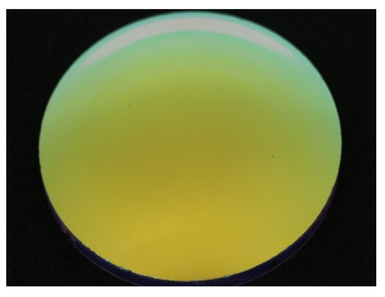
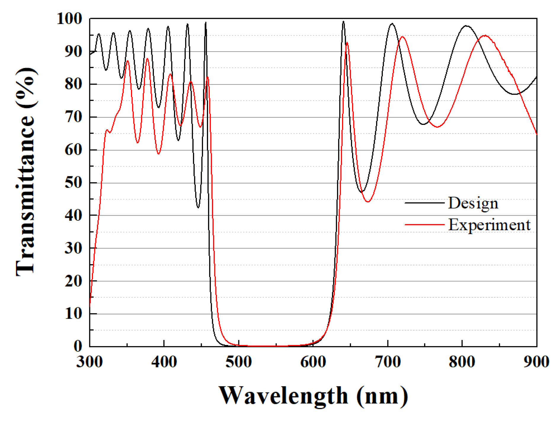
After the fabrication of multilayer notch filter, a series of tests and analysis are required. The optical transmittance, residual stress, surface roughness, and surface morphology are measured by a UV/VIS/NIR spectrophotometer, Twyman-Green interferometer, scanning probe microscope, Linnik microscopic interferometer, and field emission scanning electron microscopy (FE-SEM). Figure 1 demonstrates the picture of the 532 nm notch filter. The color change of the picture is due to the optical path difference changed by the tilt angle. From different angles, the optical interference filter shows different colors. The experimental results are compared with those simulated by Essential MacLeod software. The optical transmittance of the notch filter was measured by a Shimadzu UV-2600i spectrophotometer with a resolution of 0.1 nm. Figure 2 shows the transmission spectra of the measured and design results of the 18-layer notch filter with a center wavelength of 532 nm. It can be seen from the position of the center wavelength of the transmission spectrum that the transmittance of the notch band and the bandwidth of the notch filter are consistent with the design. The transmittance is 0.2% for the center wavelength of 532 nm. The full width at half maximum (FWHM) of the notch filter is about 100 nm, and the average transmittance of the transmission band is about 70%. For the absorbance evaluation, the optical density (OD) is a logarithmic measurement of the percent transmission (%T). In other words, optical density (OD) is the logarithmic reciprocal of transmittance. Its value is a measure of the attenuation of energy passing through a filter. The higher the OD value, the higher the attenuation and the greater the protection level. For the proposed notch filter, the optical density is 2.7 (near 3.0). As can be seen from Figure 2, the central wavelength difference between the design and experimental samples is 8 nm. The designed thickness of the notch filter is 1374 nm, but the coating thickness of the manufactured notch filter is 1449 nm, which is 75 nm thicker than the designed multilayer film. This might be an error in the thickness measurement. Therefore, compared with the designed spectral curve, the measured spectral curve of the coated sample shows a red shift from the change of the spectral curve. Using the optical monitoring is helpful for getting the designed thicknesses. However, our optical monitoring system has a thickness deviation of ±2.5%. In fact, a total thickness deviation of 5% will lead to undesirable results. The thickness deviation also affects the center wavelength (CWL) shift. Even so, the notch band characteristics of the notch filter are very similar to the design results. The reason affecting the ripple of the transmission band is that the top layer of the SiO2 film is closest to the air, so it is more sensitive to the transmittance change of the transmission band.
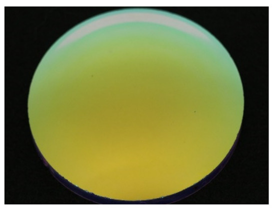
Figure 1.
The picture of the notch filter sample.
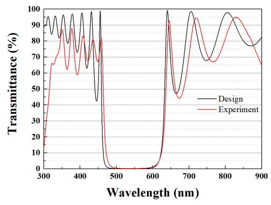
Figure 2.
Transmittance spectra of notch filter.
Figure 3 shows the results of wavefront sensing measurement on the left− and right−eye spectacle lenses. The notch filter was deposited on the spectacle lenses made of BK7 glass material. From the experimental results, the surface height of the uncoated wavefront profile of the left- and right-eye spectacle lenses can be determined by the wavefront sensing measurement. The peak-valley (PV) values of the uncoated lenses are about 43.87 μm and 42.99 μm, and the radius of curvature values are 4.09 m and 4.23 m, respectively. The PV value of the surface height after depositing the multilayer notch filter becomes 30.07 μm and 28.02 μm, and the radius of curvature values are 6.33 m and 7.07 m, respectively. The peak–valley change of the surface height is greater than the total thickness of the multilayer film: 1.37 μm. It is obvious that the spectacle lens is affected by the multilayer coatings and changes the wavefront surface profile.
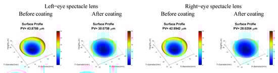
Figure 3.
Wavefront contour measurement of the notch filter for the left− and right−eye spectacle lenses.
No matter what kind of thin film preparation technology is used, the thin film will produce residual stress in the growth process, because excessive residual stress levels can dramatically affect the performance, reliability, and durability of multilayer components and devices. As the residual tensile stress is too large, the thin film will be easy to peel off or crack, and if the residual compressive stress is too large, the thin film may be wrinkled or broken. Therefore, the measurement of residual stress is one of the important mechanical properties of the multilayer films. For the residual stress measurement, the Tywman–Green interferometer was used to measure the radii of curvature before and after the 18-layer notch filter coated with high-reflection multilayer films, and then, the residual stress was calculated by the proposed method. Figure 4 indicates the 3D surface profile of the glass substrate before and after coating. The radius of curvature before coating is 174.394 ± 1.494 m, and the radius of curvature after coating is −178.401 ± 4.102 m. From the change of surface profile, it can be seen that the surface shape of the glass substrate is concave. After coating an 18-layer notch filter, the surface shape becomes convex, and the residual stress is −0.298 ± 0.004 GPa. The residual stresses of single-layer SiO2, Nb2O5 film, and multilayer notch filter were measured by the Twyman–Green interferometer, the residual compressive stresses of single-layer SiO2, Nb2O5 film are −0.590 GPa and −0.241 GPa. The residual compressive stress of the 18-layer notch filter is −0.298 GPa. Compared with the single-layer film, the multilayer film has a lower compressive stress, indicating that the source of stress contribution not only comes from the single-layer film but may also derive from the interfacial stress and thermal stress. It can be seen from these results that the residual compressive stress in the notch filter is less than 300 MPa and presents a low stress state. The results show that the notch filter has good mechanical stress characteristics.
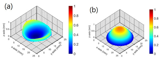
Figure 4.
Three-dimensional (3D) surface contour of the B270 glass substrate (a) before coating; (b) after coating.
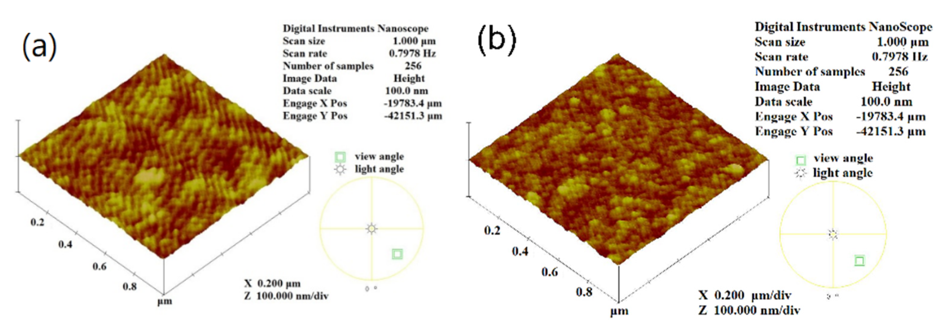
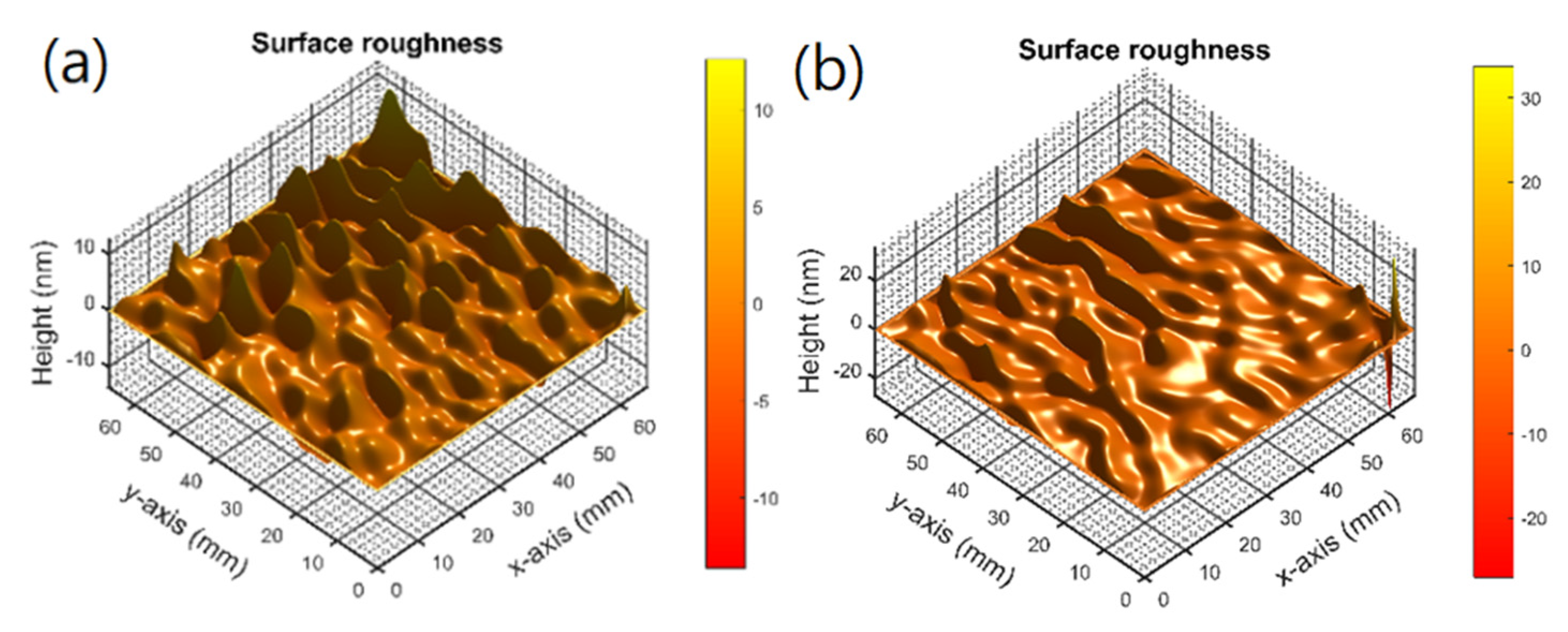
Thin film growth is a promising field in modern nano-sciences. Surface roughness typically results in the scattering of electrons or light [19]. Surface roughness is one of the thin film characteristics that need to be understood after thin film coating. The surface roughness will directly affect the amount of optical scattering, which will seriously reduce the transmittance of the optical filter, so a good optical interference filter has the characteristic of low surface roughness. In this work, two measuring instruments are used to determine the surface roughness of the sample. One is a scanning probe microscope (SPM), the other is a self-developed Linnik microscopic interferometer. Figure 5 shows the surface roughness of the notch filter by using SPM. The root mean square (rms) surface roughness of the sample is 2.15 nm before coating and 1.71 nm after coating the multilayer notch filter. Furthermore, the rms surface roughness is also determined by the Linnik microscopic interferometer. Figure 6 shows the surface roughness of the substrate before coating is 2.18 nm, and the surface roughness of the substrate after coating is reduced to 1.88 nm. The surface roughness values of the notch filter measured by the two different instruments are consistent. These results show that the notch filter has a smooth surface and low surface roughness. When different types of measurements on the same sample are converted to rms roughness and compared, because the spatial frequency and bandwidth limitations of the instrument are different, the measured values are usually different as well.
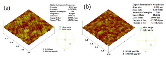
Figure 5.
Surface roughness map of the sample measured by AFM (a) before coating; (b) after coating.
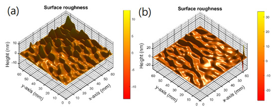
Figure 6.
Surface roughness map of the sample measured by Linnik microscopic interferometer (a) before coating; (b) after coating.
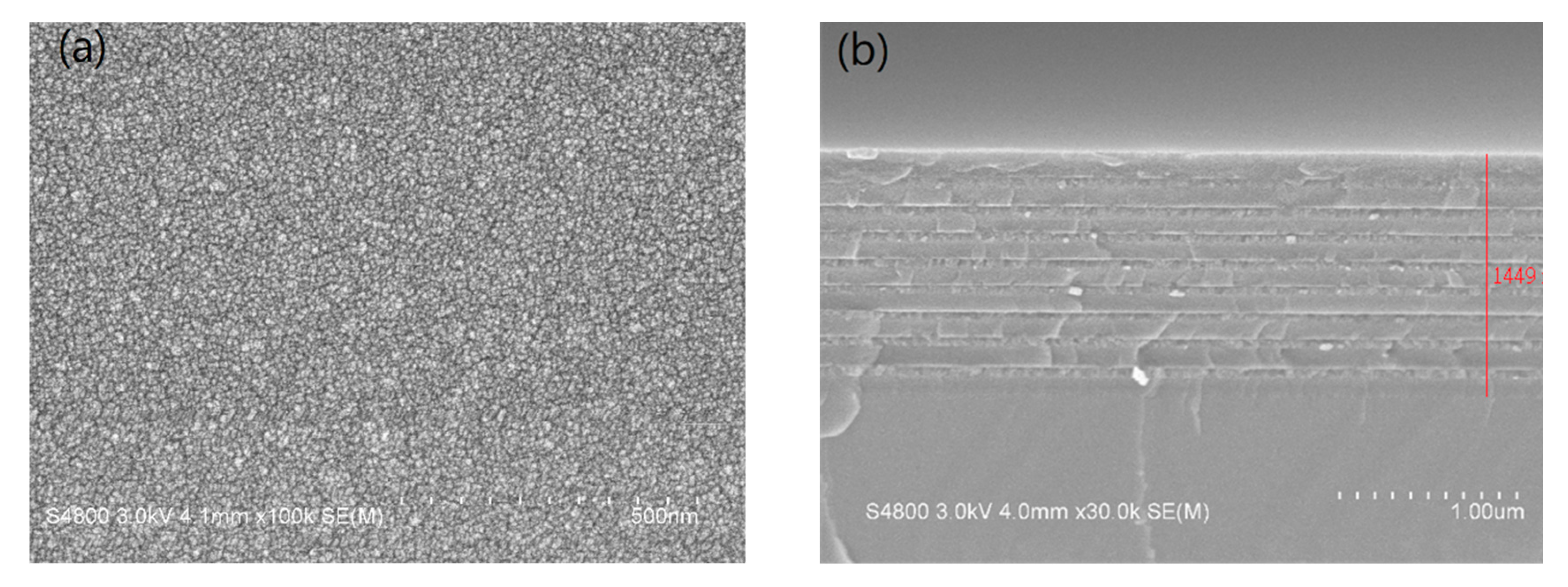
In addition, from the transmittance spectrum, the difference between the designed peak–to–valley (PV) value and the measured spectral transmittance is very small, so the measured surface roughness value will not seriously affect the transmittance of the notch filter. The resulting surfaces can be imaged by scanning electron microscopy (SEM). Figure 7 shows the SEM micro–image of the notch filter with a center wavelength of 532 nm. Each layer can be clearly observed. The black interface is the SiO2 film, and the gray one is the Nb2O5 film. The SEM micro–image indicates that the SiO2 film structure is continuous and dense. In the Nb2O5 film, a relatively discontinuous columnar structure is observed from the SEM micrograph, which is consistent with the measurement results of residual stress. It is worth noting that a slight columnar structure can be observed in the first and third layers of SiO2 film, while the structure of the fifth, seventh, and ninth layers gradually becomes dense, which may mean that the compressive stress of the multi–layer notch filter will be more significant with the increase of the number of layers.

Figure 7.
SEM micro–images of the notch filter (a) top view; (b) cross–section view.
4. Conclusions
In this study, the objective is to understand the optical properties, mechanical properties, and surface characteristics of the notch filters prepared by electron beam evaporation combined with ion-assisted deposition method. A notch filter with a center wavelength of 532 nm have been designed and fabricated. The 18-layer notch filter design for the laser protective lenses was simulated by Essential Macleod software. The transmittance of the center wavelength is 0.2%, the bandwidth (FWHM) of the notch filter is about 100 nm, and the average transmittance of the transmission band is about 70%. For the absorbance evaluation, the optical density is a logarithmic measurement of the percent transmission (%T). The optical density is 2.7 for the proposed notch filter. For the wavefront contour measurement of the laser protective lens, the multilayer notch filter is deposited on the laser protective spectacle lens (concave lens). The results show the peak-to-valley value of the wavefront contour of the concave lens changes: 13 μm. This value is greater than the B270 flat glass coated with a 1.37 μm thick multilayer thin film. Obviously, the change of wavefront profile of spectacle lenses is affected by multilayer coatings. For the mechanical properties, the residual compressive stress of the multilayer notch filter is 0.298 GPa. Compared with the single-layer film, the compressive stress of the multilayer film is smaller. The results show that the contribution of residual stress comes not only from the single-layer thin film but also from the interfacial stress in the multilayer structure [20]. It can be seen from the stress measurement results that the residual compressive stress is less than 0.30 GPa. The root-mean-square surface roughness of the multilayer notch filters was measured by SPM. The surface roughness value was 2.15 nm before coating and 1.71 nm after coating. Similarly, the surface roughness of the sample was measured by the Linnik microscopic interferometer. The surface roughness of the sample before coating is 2.18 nm, and the surface roughness of the sample after coating is reduced to 1.88 nm. We can see from the 3D surface contour maps that the surface flatness after coating is quite smooth. It also can be seen from the SEM micro-image that the surface morphology of the notch filter is smooth and dense. These results demonstrate a new 532 nm laser protective lens based on optical multilayer notch filter design with low residual stress and low surface roughness.
Author Contributions
Conceptualization and methodology, C.-L.T.; writing—review and editing, C.-L.T.; filter design and measurement, H.-Y.L.; coating experiment and data analysis, K.-S.C.; data curation, C.-K.C. All authors have read and agreed to the published version of the manuscript.
Funding
This research was funded by Ministry of Science and Technology of Taiwan for their financial support of this research under Contract number MOST 110-2221-E-035-061. This study was financially supported by Feng Chia University (Contract No. 20H00308).
Institutional Review Board Statement
Not applicable.
Informed Consent Statement
Not applicable.
Data Availability Statement
Not applicable.
Acknowledgments
The authors are grateful for the Precision Instrument Support Center of Feng Chia University in providing SEM analytical facilities.
Conflicts of Interest
The authors declare no conflict of interest.
References
- Zhang, J.; Tikhonravov, A.V.; Trubetskov, M.K.; Liu, Y.; Cheng, X.; Wang, Z. Design and fabrication of ultra-steep notch filters. Opt. Express 2013, 21, 21523–21529. [Google Scholar] [CrossRef] [PubMed]
- Tikhonravov, A.V.; Trubetskov, M.K.; Amotchkina, T.V.; Kokarev, M.A.; Kaiser, N.; Stenzel, O.; Wilbrandt, S.; Gäbler, D. New optimization algorithm for the synthesis of rugate optical coatings. Appl. Opt. 2006, 45, 1515–1524. [Google Scholar] [CrossRef] [PubMed]
- Allan, S.T.; Herrington, B.; Cole, C.; Mackrodt, K.; Slim, T.; Lingwood, D. Rugate coating for an avionics head-up-display. In Defense, Security, and Cockpit Displays; International Society for Optics and Photonics: Bellingham, WA, USA, 2004; Volume 5443, pp. 130–137. [Google Scholar]
- Piegari, A.; Flory, F. Optical Thin Films and Coatings: From Materials to Applications; Woodhead: Sawston, UK, 2018. [Google Scholar]
- Kumar, V.S.P.; Kumar, M.; Kumari, N.; Sharma, A.L. Design and development of an optical reflective notch filter using the ion assisted deposition technique with stepwise modulated thickness for avionics applications. Appl. Opt. 2020, 59, 564–571. [Google Scholar] [CrossRef] [PubMed]
- Shankar, A.; Kumar, S. Using a pair of antireflection layer in a minus filter to suppress ripples in the HUD-beam combiner. J. Opt. 2014, 43, 257–259. [Google Scholar] [CrossRef]
- Richter, F.; Kupfer, H.; Schlott, P.; Gessner, T.; Kaufmann, C. Optical properties and mechanical stress in SiO2/Nb2O5 multilayers. Thin Solid Films 2001, 389, 278–283. [Google Scholar] [CrossRef]
- Scherer, M.; Schallenberg, U.; Zoeller, A. High performance Notch Filter Coatings produced with PIAD and Magnetron. In Advances in Optical Thin Films III; International Society for Optics and Photonics: Bellingham, WA, USA, 2008; Volume 7101, p. 710101-10. [Google Scholar]
- Zhang, J.; Xie, Y.; Cheng, X.; Jiao, H.; Wang, Z. Thin-film thickness modulated designs for optical minus filters. Appl. Opt. 2013, 52, 5788–5793. [Google Scholar] [CrossRef] [PubMed]
- Lyngnes, O.; Kraus, J. Design of optical notch filters using apodized thickness modulation. Appl. Opt. 2014, 53, A21–A26. [Google Scholar] [CrossRef] [PubMed]
- Hoggan, R.N.; Subhash, A.; Blair, S.; Digre, K.B.; Baggaley, S.K.; Gordon, J.; Brennan, K.C.; Warner, J.E.A.; Crum, A.V.; Katz, B.J. Thin-film optical notch filter spectacle coatis for the treatment of migraine and photophobia. J. Clin. Neurosci. 2016, 28, 71–76. [Google Scholar] [CrossRef] [PubMed] [Green Version]
- Kumar, M.; Kumari, N.; Sharma, A.L.; Karar, V.; Sinha, R.K. Design and fabrication of reflective notch filter using modified thickness modulated Al2O3-SiO2 multilayer. In Optical Interference Coatings; Optical Society of America: Washington, DC, USA, 2019. [Google Scholar]
- MacLeod, H.A. Thin-Film Optical Filters, 4th ed.; CRC Press: Boca Raton, FL, USA, 2010. [Google Scholar]
- Tien, C.L.; Zeng, H.D. Measuring residual stress of anisotropic thin film by fast Fourier transform. Opt. Express 2010, 18, 16594–16600. [Google Scholar] [CrossRef] [PubMed]
- Takeda, M.; Ina, H.; Kobayashi, S. Fourier-transform method of fringe-pattern analysis for computer-based topography and interferometry. Appl. Opt. 1982, 72, 156–160. [Google Scholar] [CrossRef]
- Stoney, G.G. The tension of metallic films deposited by electrolysis. Proc. R. Soc. Lond. 1909, 86, 172–175. [Google Scholar]
- Tien, C.L.; Yang, H.M.; Liu, M.C. The measurement of surface roughness of optical thin films based on fast Fourier transform. Thin Solid Film 2009, 517, 5110–5115. [Google Scholar] [CrossRef]
- Tien, C.L.; Yu, K.C.; Tsai, T.Y.; Lin, C.S.; Li, C.Y. Measurement of surface roughness of thin films by a hybrid interference microscope with different phase algorithms. Appl. Opt. 2014, 53, H213–H219. [Google Scholar] [CrossRef] [PubMed]
- Elsholz, F.; Schöll, E.; Rosenfeld, A. Control of surface roughness in amorphous thin-film growth. Appl. Phys. Lett. 2004, 84, 4167–4169. [Google Scholar] [CrossRef]
- Tien, C.L.; Chen, K.P.; Lin, H.Y. Internal stress prediction and measurement of mid-infrared multilayer thin films. Materials 2021, 14, 1101. [Google Scholar] [CrossRef] [PubMed]


Publisher’s Note: MDPI stays neutral with regard to jurisdictional claims in published maps and institutional affiliations. |
© 2021 by the authors. Licensee MDPI, Basel, Switzerland. This article is an open access article distributed under the terms and conditions of the Creative Commons Attribution (CC BY) license (https://creativecommons.org/licenses/by/4.0/).