Abstract
Structural coloration based on nanostructures is one of the alternatives that can prevent environmental pollution compared to the use of chemically synthesized materials. This technique has attracted considerable attention for various applications, including displays and sensors. In this study, a photonic crystal structure based on spherical silica was formed to provide structural color using an electro-hydrodynamic (EHD) equipment, a printed electronic system attracting considerable interest. The EHD inkjet printing equipment could print micro- and nanostructures using the voltage applied between the nozzle and substrate. Silica-based ink samples were prepared for use in the EHD equipment. Appropriate printing parameters for the EHD inkjet printing were set using the prepared sample. Spherical silica was printed on a polyimide (PI) film layer. The spherical silica nanoparticles discharged during the EHD inkjet printing were not deformed by the EHD process. A photonic crystal structure was formed on a polydimethylsiloxane (PDMS) layer by EHD printing by covering the PDMS layer on the PI film. The spherical-silica-based photonic crystal structure formed on the PDMS layer with elasticity and flexibility exhibited a color change with bending loads.
1. Introduction
Generally, color is expressed using dyes and pigments obtained by chemical syntheses. The dyes and pigments, such as azo dyes, have toxic and carcinogenic substances fatal to the human body. They not only affect humans but also lead to high environmental pollution. To overcome the shortcomings of dyes and pigments, various companies and research institutes have carried out studies on materials and technologies that decompose chemical synthetic drugs and implement colors in an environmentally friendly manner [1,2,3,4,5,6,7,8,9,10]. In particular, structural colors and photonic crystals using fine structural features (not colors obtained by chemical syntheses), such as chameleons, opals, beetle shells, and morpho-butterflies commonly found in nature, have attracted considerable attention [11,12,13,14,15]. Structural color is generally based on the principle of band gap and interference, where for light in the visible-light region, which can be recognized by the human eye, a specific wavelength is reflected while passing through a photonic crystal structure [16,17,18]. The structural color approach using the above principle has the advantage of continuously expressing color as long as the photonic crystal is not destroyed on the surface of the object. Utilizing the above characteristics, studies have been recently carried out to combine structural color and photonic crystal structure with displays, sensors, and camera resolution [19,20,21]. However, to express the structural color and structural features that are the core of photonic crystals, technologies are required to fabricate micro- and nanostructures [22]. In most cases, lithography and dip coating are used for the formation of micro- and nanostructures. Lithography is used in the semiconductor industry for fabrication of nanostructures on silicon wafers. However, the initial cost due to the equipment is high, so that the experiment cannot be carried out in a small-scale laboratory. In addition, the amount of consumed material is large. In the case of dip coating, because nanostructures are formed using attraction and repulsion between molecules, it is simple and has a low initial cost. However, complex structures are challenging to fabricate; only simple nanostructures can be fabricated [23,24,25,26,27].
Owing to these shortcomings, electro-hydrodynamic (EHD) printing, a printing electronic technology, has recently attracted considerable interest in various industries. The EHD method creates an electric field at the tip of the nozzle by applying a voltage between the nozzle and substrate. As the meniscus of the ink at the tip of the nozzle in which the electric field is formed is changed by the force of electricity, micro- and nanostructures can be manufactured with smaller sizes than that of the nozzle. In addition, it can be used to design various complex circuits by synthesizing electronic materials and grafting them to the EHD ink. In addition, extensive studies on flexible displays, polymer flexible radio-frequency identification, polymer flexible solar cells, and thin-film transistors using EHDs are ongoing. In the EHD method, the amount of used material is remarkably small, so that the amount of chemical waste can be largely reduced, which is expected to reduce the cost and reduce environmental pollution [28,29,30,31,32,33,34,35,36,37].
With the development of printing electronic technologies such as the EHD technology, polydimethylsiloxane (PDMS), a silicone-based polymer material, has attracted considerable attention. PDMS has a high durability owing to its low plastic deformation rate and transparent properties at small thicknesses, flexibility, and elasticity. By utilizing the above advantages and EHD method, extensive studies have been carried out using grafting on mobile, flexible, and wearable displays and electronic materials [38,39,40].
In this study, an experiment was carried out using PDMS and EHD method by synthesizing silica particles from opal components reflecting various colors. Spherical silica particles used for EHD inkjet printing were synthesized using Stöber ink. The ink was prepared by synthesizing spherical silica particles and solvent. The synthesized ink was used for EHD inkjet printing to produce a photonic crystal structure formed using spherical silica nanoparticles on a polyimide (PI) film layer. The PI film layer, on which the photonic crystal structure was formed, was deposited on PDMS. The characteristics of the silica-based photonic crystal structure deposited on the PDMS were evaluated.
2. Materials and Methods
2.1. Reagents and Instruments
To generate spherical silica, ammonia (28.0–30%, Samchun, Korea), ethanol (EtOH, 95%, Ducksan, Korea), deionized (DI) water (extra pure grade, Ducksan, Korea), and tetraethyl orthosilicate (TEOS, 95%, Ducksan, Korea) were used. The synthesis of silica nanoparticles was confirmed by X-ray diffraction (XRD, Malvern Panalytical, Almelo, The Netherlands). For the EHD method (ENJET, Suwon, Korea), a silica-based nanostructure was formed using ethylene glycol (99.9%, Samchun, Korea) as a solvent. In addition, a nozzle (NanoNC, Seoul, Korea) with an ID size of 0.15 mm and an OD size of 0.30 mm was used as the nozzle for EHD. PDMS (Sylgard 184, DOW Corning, Yangsan, Korea) was used to completely separate the structure of the PI film. Field-emission scanning electron microscopy (FE-SEM, S-4700, Hitachi, Tokyo, Japan) was used to evaluate the dimensions of the nanostructures and silica particles formed on the PDMS.
2.2. Silica Nanoparticles
Table 1 shows the amounts of the samples used for the silica synthesis. In addition, Figure 1 illustrates the silica nano particle manufacturing using the Stöber method [41]. To hydrolyze DI water and ethanol, stirring was performed at 65 °C and 540 rpm on a heating plate [23,24]. TEOS was added to the DI water and ethanol aqueous solution, followed by stirring at 65 °C and 540 rpm for 10 min. The stirring was performed for 10 min at 540 rpm to form silica particles. To obtain an intact silica powder, the resulting solution was aged for 24 h. The solution after the aging was separated in a centrifuge at 3000 rpm for 1 h to separate the silica particles. The separated silica particles were dried in a convection oven at 50 °C for 6 h to obtain the spherical silica nanoparticle powder.

Table 1.
Reagents used in the synthesis of spherical silica nanoparticles.
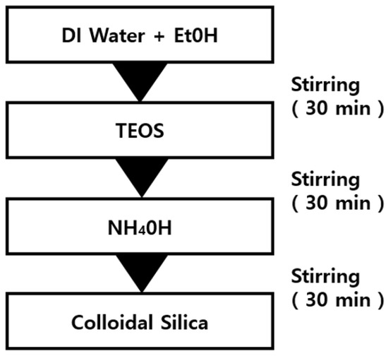
Figure 1.
Manufacturing process of spherical silica nanoparticles.
2.3. EHD Inkjet Printing on the PI Film
Figure 2 shows the configuration of the EHD inkjet system. It consists of a syringe pump, high-voltage amplifier, three-axis driving system, patterning head, and process control system as the main module. In addition, the submodule consists of a charge-coupled device (CCD) camera and light-emitting diode lighting. The flow rate was set using the syringe pump. The parameters of the EHD printing were adjusted using a computer. Using the CCD camera, it was possible to immediately check the shape of the ink discharged from the nozzle and control the shape of the ink.
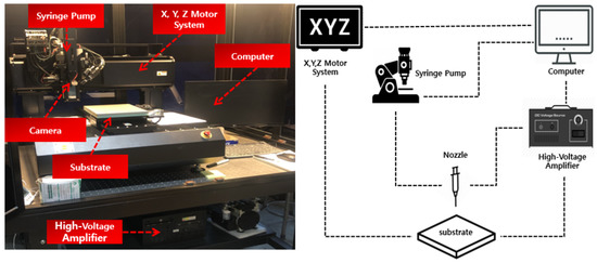
Figure 2.
Configuration of the electrohydrodynamic (EHD) inkjet system.
Figure 3 illustrates the nozzle part during the EHD inkjet printing. An electric field was generated by applying a high voltage between the nozzle and substrate of the inkjet printing head. The ink was moved in the direction of the electric force using the interaction with the induced electric charge in the ink. Electric charges accumulated on the surface of the fluid owing to the generated electrostatic effect. Upon saturation, the fluid was separated from the nozzle and discharged. The three-axis driving equipment moved in the desired direction to print.
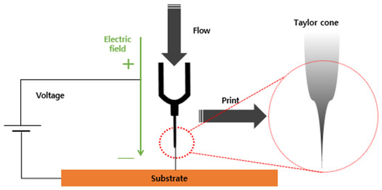
Figure 3.
Schematic diagram of the EHD inkjet nozzle.
Figure 4 shows the overall process for the printing of silica particles on the PI film using the EHD inkjet printer. Ethylene glycol and silica nanoparticle powder were mixed to prepare the silica nano-ink for the EHD inkjet printing. The mixed ethylene glycol and silica nanoparticles were stirred and dispersed for 30 min using a stirrer and ultrasonic grinder equipment to prepare a silica sample for use in the EHD ink.
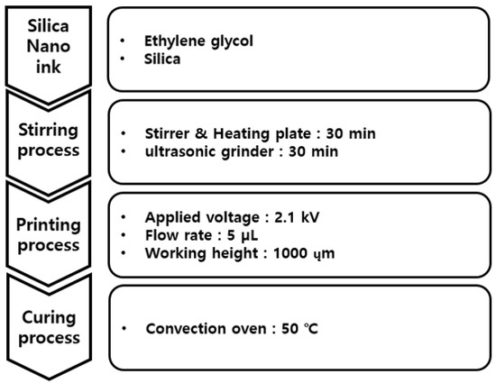
Figure 4.
Conditions of EHD inkjet printing for silica nanoparticles.
Figure 5 shows a photograph of the ejection type of the silica nano-ink according to the voltage during the printing illustrated in Figure 4. The silica nano-ink can have dripping, cone jet, and whipping forms according to the voltage of the EHD printer. During the printing, when the silica nano-ink was ejected onto the PI film, a voltage of 2.1 kV and cone-jet shape were observed, which shows an optimal voltage of 2.1 kV. The flow rate was 5 µL, the working height was 1000 µm, and the voltage was 2.1 kV. The discharged PI film was cured in a convection oven for 40 min, as shown in Figure 3.
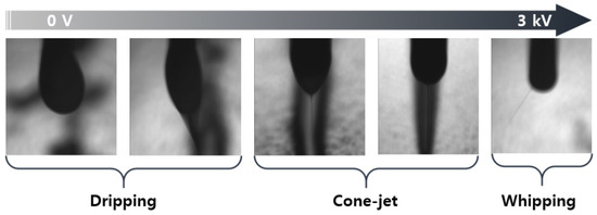
Figure 5.
Silica nano-ink discharged from the EHD inkjet printing nozzle at various voltages.
2.4. PDMS-Based Structural Color
Figure 6 illustrates the fabrication of PDMS using the base and curing agents. The PDMS base and PDMS curing agent were mixed for 10 min at a weight ratio of 7:1 (g), and then poured into a mold to fix. The air bubbles generated during the mixing were removed using a vacuum pump at 670 mmHg for 60 min. The bubble-removed PDMS was subjected to a curing process in a convection oven at 50 °C.

Figure 6.
Manufacturing of polydimethylsiloxane (PDMS) layer.
Figure 7 shows a photograph of only the PDMS layer created by the process illustrated in Figure 6. Figure 7a shows that the fabricated PDMS is transparent at thickness of 5 mm. Figure 7b presents an SEM image of the fabricated PDMS layer, which shows that the PDMS layer was well fabricated without surface defects.
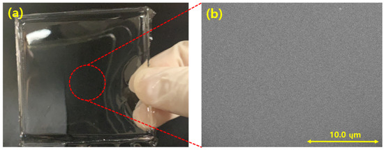
Figure 7.
(a) PDMS layer; (b) field emission scanning electron microscopy (FE-SEM) image of the PDMS surface.
Figure 8 illustrates the process of formation of silica nanoparticles discharged on the PI film inside the PDMS layer. PDMS in liquid form after mixing was formed on the PI film layer where the curing processes were completed. Bubbles formed in the PDMS layer in the liquid state were removed for 1 h using a vacuum pump. The PDMS, from which air bubbles were removed, was cured in a convection oven at 50 °C for 6 h. After the curing, the PDMS removed the PI film. The fabricated PDMS was manufactured with a width of 60 mm, length of 60 mm, and thickness of 5 mm.
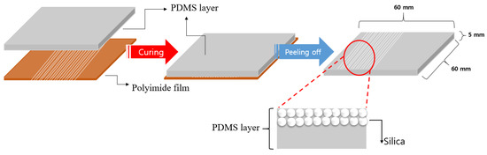
Figure 8.
Process of forming silica nanoparticles inside the PDMS layer.
3. Results and Discussion
3.1. Silica Nanoparticles
Figure 9 shows an XRD pattern to analyze the formation of spherical silica nanoparticles. The silica particles exhibited a peak at 20–30°, which confirms their successful synthesis [42].
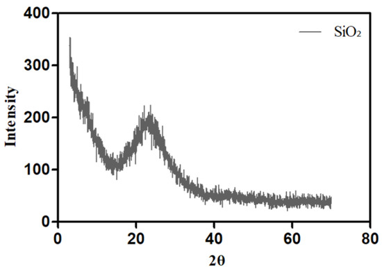
Figure 9.
X-ray diffraction (XRD) pattern of the synthesized silica nanoparticles.
Figure 10 shows FE-SEM images of the produced silica powder, which confirm that the silica particles used in the EHD inkjet printing had a spherical shape. Furthermore, in Figure 10b there is an enlarged photograph of the red part of Figure 10a. Figure 11 is a graph confirming the distribution of silica particles. As a result of confirming the distribution of the silica particle size, it was confirmed that the size of the spherical silica particles was distributed around an average of 400 nm.
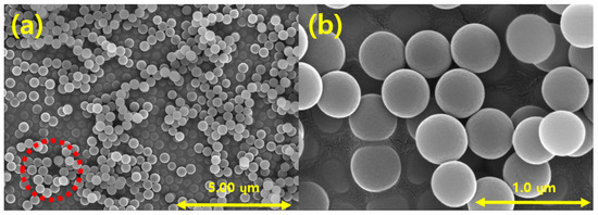
Figure 10.
FE-SEM images of the synthesized silica nanoparticles at magnifications of (a) 10.0 k; (b) 50.0 k.
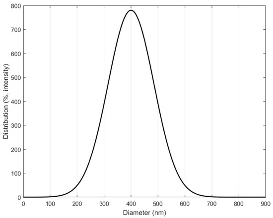
Figure 11.
Particle sizes of silica distributions.
3.2. EHD Inkjet Printing
Figure 12 presents SEM images showing the ejection of spherical silica nanoparticles into the PI film layer using the EHD inkjet printer. Figure 12a,b show the overall shape of the silica-based ink discharged on the PI film layer. Figure 12a confirms that the range of the silica ink discharged on the PI film was approximately 400 µm. Figure 12b shows the arrangement of the silica particles, which are the constituents of the ink discharged on the PI film. The spherical silica particles were normally discharged by the EHD inkjet printing, as shown in Figure 12c. The shapes and sizes of the silica nanoparticles were not affected during the discharging to the PI film and curing.
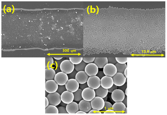
Figure 12.
FE-SEM images of silica particles printed using the EHD inkjet printer on the polyimide (PI) film at magnifications of (a) 180; (b) 5.00 k; (c) 50.0 k.
3.3. Stretching of PDMS
Figure 13a,b show images of PDMS manufactured through the process illustrated in Figure 8. Figure 13a shows the spherical silica nanoparticles bonded inside the PDMS layer. In addition, Figure 13a was taken without bending the PDMS. Figure 13b shows an FE-SEM image of the silica nanoparticles formed in the PDMS. These images confirm that the silica particles discharged on the PI film layer were formed inside the PDMS.
Figure 13.
Silica nanoparticles formed inside the PDMS layer: (a) image without bending; (b) FE-SEM image of the silica nanoparticles formed inside the PDMS.
Figure 14 shows an image and color change according to the bending of the PDMS on which silica particles were deposited. Figure 14a shows a photograph of the spherical silica particles discharged with the EHD inkjet printer, which led to a color change upon the bending inside the PDMS. However, when there is no bending in PDMS, silica particles cannot form a photonic crystal structure, so only silica particles are visible inside the PDMS. Upon the bending, as shown in Figure 14b, the arrangement of the silica particles changed and the color changed according to the angle. When the PDMS is bent, the arrangement of spherical silica particles is changed, forming a silica-based photonic crystal, reflecting light in the visible region and providing structural color.
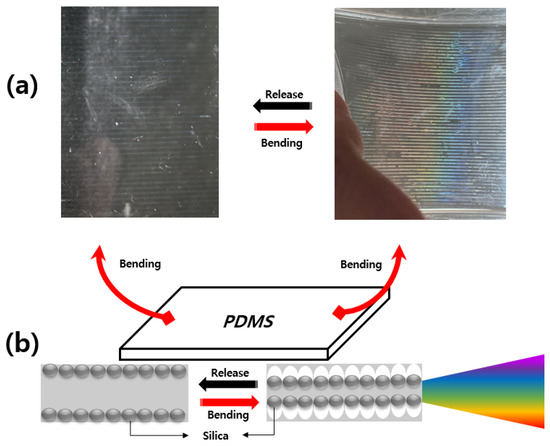
Figure 14.
Formation of a photonic crystal structure upon the bending: (a) color change upon the bending; (b) schematic diagram of the changes in silica particles formed inside the PDMS with the bending loads.
4. Conclusions
In this study, EHD inkjet printing and spherical silica particles were used to form a photonic crystal structure inside the PDMS. To prepare a sample for use as an EHD inkjet printing ink, spherical silica nanoparticles were produced by the Stöber method. The formation of silica nanoparticles was confirmed and their sizes were evaluated using SEM and XRD. Spherical silica particles were mixed with ethylene glycol to prepare samples for use in the EHD inkjet printing. The optimal ejection was performed on the PI film layer by adjusting the height, flow rate, and voltage parameters of the silica-based ink and EHD samples. The SEM images showed that when the silica particles were discharged with the EHD printer, the size and shape of the powdered silica were not affected. A PDMS layer was formed on the PI film, on which the curing was completed. Silica particles discharged on the PI film layer were formed inside the PDMS. In addition, the SEM images confirmed that the discharged lines were formed on the PI film layer inside the PDMS. The silica particle line formed inside the PDMS did not form a photonic crystal when bending was not applied. However, when the PDMS with elasticity and flexibility was bent, the silica particles formed a photonic crystal and exhibited structural color. Various colors were observed according to the bending and angle. The printing of spherical silica nanoparticles using the EHD inkjet printer confirmed that nanostructure fabrication can be achieved.
Author Contributions
J.-H.C.: Conceptualization, investigation, methodology, writing. J.-H.A.: writing. C.-Y.L.: Conceptualization, project administration, methodology, supervision, review and editing. All authors have read and agreed to the published version of the manuscript.
Funding
This research was supported by the Basic Science Research Program through the National Research Foundation of Korea (NRF) funded by the Ministry of Education (2019R1I1A3A01060180).
Institutional Review Board Statement
Not applicable.
Informed Consent Statement
Not applicable.
Data Availability Statement
Data are contained within the article.
Conflicts of Interest
The authors declare no conflict of interest.
References
- Berradi, M.; Hsissou, R.; Khudhair, M.; Assouag, M.; Cherkaoui, O.; Bachiri, A.; Harfi, A. Textile finishing dyes and their impact on aquatic environs. Heliyon 2019, 5, e02711. [Google Scholar] [CrossRef]
- Lellis, B.; Fávaro-Polonio, C.Z.; Pamphile, J.A.; Polonio, J.C. Effects of textile dyes on health and the environment and bioremediation potential of living organisms. Biotechnol. Res. Innov. 2019, 3, 275–290. [Google Scholar] [CrossRef]
- Chequer, F.M.D.; Angeli, J.P.F.; Ferraz, E.R.A.; Tsuboy, M.S.; Marcarini, J.C.; Mantovani, M.S.; de Oliveira, D.P. The azo dyes Disperse Red 1 and Disperse Orange 1 increase the micronuclei frequencies in human lymphocytes and in HepG2 cells. Mutat. Res. Genet. Toxicol. Environ. Mutagenes. 2009, 676, 83–86. [Google Scholar] [CrossRef]
- Deogaonkar, S.C.; Wakode, P.; Rawat, K.P. Electron beam irradiation post treatment for degradation of non biodegradable contaminants in textile wastewater. Radiat. Phys. Chem. 2019, 165, 108377. [Google Scholar] [CrossRef]
- Khan, S.; Malik, A. Toxicity evaluation of textile effluents and role of native soil bacterium in biodegradation of a textile dye. Environ. Sci. Pollut. Res. 2018, 25, 4446–4458. [Google Scholar] [CrossRef]
- Khandare, R.V.; Govindwar, S.P. Phytoremediation of textile dyes and effluents: Current scenario and future prospects. Biotechnol. Adv. 2015, 33, 1697–1714. [Google Scholar] [CrossRef] [PubMed]
- Khatri, J.; Nidheesh, P.V.; Singh, T.A.; Kumar, M.S. Advanced oxidation processes based on zero-valent aluminium for treating textile wastewater. Chem. Eng. J. 2018, 348, 67–73. [Google Scholar] [CrossRef]
- Wei, F.; Shahid, M.J.; Alnusairi, G.S.; Afzal, M.; Khan, A.; El-Esawi, M.A.; Abbas, Z.; Wei, K.; Zaheer, I.E.; Rizwan, M.; et al. Implementation of Floating Treatment Wetlands for Textile Wastewater Management: A Review. Sustainability 2020, 12, 5801. [Google Scholar] [CrossRef]
- Akhtar, M.F.; Ashraf, M.; Anjum, A.A.; Javeed, A.; Sharif, A.; Saleem, A.; Akhtar, B. Textile industrial effluent induces mutagenicity and oxidative DNA damage and exploits oxidative stress biomarkers in rats. Environ. Toxicol. Pharmacol. 2016, 41, 180–186. [Google Scholar] [CrossRef] [PubMed]
- de Lima, R.O.A.; Bazo, A.P.; Salvadori, D.M.F.; Rech, C.M.; de Palma Oliveira, D.; de Aragão Umbuzeiro, G. Mutagenic and carcinogenic potential of a textile azo dye processing plant effluent that impacts a drinking water source. Mutat. Res. Genet. Toxicol. Environ. Mutagenes. 2007, 626, 53–60. [Google Scholar] [CrossRef]
- Shi, X.; He, J.; Xie, X.; Dou, R.; Lu, X. Photonic crystals with vivid structure color and robust mechanical strength. Dye. Pigment. 2019, 165, 137–143. [Google Scholar] [CrossRef]
- Chung, K.; Yu, S.; Heo, C.J.; Shim, J.W.; Yang, S.M.; Han, M.G.; Lee, S.H.; Jin, Y.; Lee, Y.S.; Park, N.; et al. Flexible, angle-independent, structural color reflectors inspired by Morpho butterfly wings. Adv. Mater. 2012, 24, 2375–2379. [Google Scholar] [CrossRef]
- Kinoshita, S.; Yoshioka, S.; Fujii, Y.; Okamoto, N. Photophysics of structural color in the Morpho butterflies. Forma 2002, 17, 103–121. [Google Scholar]
- Wang, Y.; Cui, H.; Zhao, Q.; Du, X. Chameleon-inspired structural-color actuators. Matter 2019, 1, 626–638. [Google Scholar] [CrossRef]
- Teyssier, J.; Saenko, S.V.; Van Der Marel, D.; Milinkovitch, M.C. Photonic crystals cause active colour change in chameleons. Nat. Commun. 2015, 6, 1–7. [Google Scholar] [CrossRef]
- Pursiainen, O.L.; Baumberg, J.J.; Winkler, H.; Viel, B.; Spahn, P.; Ruhl, T. Nanoparticle-tuned structural color from polymer opals. Opt. Express 2007, 15, 9553–9561. [Google Scholar] [CrossRef] [PubMed]
- Kok, M.H.; Ma, R.; Lee, J.C.W.; Tam, W.Y.; Chan, C.T.; Sheng, P.; Cheah, K.W. Photonic band gap effect and structural color from silver nanoparticle gelatin emulsion. Phys. Rev. E 2005, 72, 047601. [Google Scholar] [CrossRef] [PubMed]
- Kubo, S.; Gu, Z.Z.; Takahashi, K.; Fujishima, A.; Segawa, H.; Sato, O. Tunable photonic band gap crystals based on a liquid crystal-infiltrated inverse opal structure. J. Am. Chem. Soc. 2004, 126, 8314–8319. [Google Scholar] [CrossRef]
- Zhang, J.; Meng, Z.; Liu, J.; Chen, S.; Yu, Z. Spherical colloidal photonic crystals with selected lattice plane exposure and enhanced color saturation for dynamic optical displays. ACS Appl. Mater. Interfaces 2019, 11, 42629–42634. [Google Scholar] [CrossRef] [PubMed]
- Shevtsova, E.; Hansson, C.; Janzen, D.H.; Kjærandsen, J. Stable structural color patterns displayed on transparent insect wings. Proc. Natl. Acad. Sci. USA 2011, 108, 668–673. [Google Scholar] [CrossRef] [PubMed]
- Kim, J.B.; Lee, S.Y.; Lee, J.M.; Kim, S.H. Designing structural-color patterns composed of colloidal arrays. Acs Appl. Mater. Interfaces 2019, 11, 14485–14509. [Google Scholar] [CrossRef] [PubMed]
- Li, W.; Wang, Y.; Li, M.; Garbarini, L.P.; Omenetto, F.G. Inkjet printing of patterned, multispectral, and biocompatible photonic crystals. Adv. Mater. 2019, 31, 1901036. [Google Scholar] [CrossRef] [PubMed]
- Choi, D.S.; Choi, J.H.; Lee, C.Y. Structural colors based on amorphous arrays with solely of silica particles. Appl. Sci. 2020, 10, 420. [Google Scholar] [CrossRef]
- Choi, J.H.; Choi, D.S.; Ahn, J.H.; Lee, C.Y. Biomimetic structural coloration based on spherical silica nanoparticles. J. Nanosci. Nanotechnol. 2021. Accepted for publication. [Google Scholar]
- Pease, R.F.; Chou, S.Y. Lithography and other patterning techniques for future electronics. Proc. IEEE 2008, 96, 248–270. [Google Scholar] [CrossRef]
- Brinker, C.J.; Frye, G.C.; Hurd, A.J.; Ashley, C.S. Fundamentals of sol-gel dip coating. Thin Solid Films 1991, 201, 97–108. [Google Scholar] [CrossRef]
- Faustini, M.; Louis, B.; Albouy, P.A.; Kuemmel, M.; Grosso, D. Preparation of sol− gel films by dip-coating in extreme conditions. J. Phys. Chem. C 2010, 114, 7637–7645. [Google Scholar] [CrossRef]
- Huang, Q.; Zhu, Y. Printing conductive nanomaterials for flexible and stretchable electronics: A review of materials, processes, and applications. Adv. Mater. Technol. 2019, 4, 1800546. [Google Scholar] [CrossRef]
- Lee, K.H.; Lee, S.S.; Ahn, D.B.; Lee, J.; Byun, D.; Lee, S.Y. Ultrahigh areal number density solid-state on-chip microsupercapacitors via electrohydrodynamic jet printing. Sci. Adv. 2020, 6, eaaz1692. [Google Scholar] [CrossRef]
- Cui, Z.; Han, Y.; Huang, Q.; Dong, J.; Zhu, Y. Electrohydrodynamic printing of silver nanowires for flexible and stretchable electronics. Nanoscale 2018, 10, 6806–6811. [Google Scholar] [CrossRef]
- Li, Z.; Al-Milaji, K.N.; Zhao, H.; Chen, D.R. Electrohydrodynamic (EHD) jet printing with a circulating dual-channel nozzle. J. Micromech. Microeng. 2019, 29, 035013. [Google Scholar] [CrossRef]
- Rahman, K.; Khan, A.; Muhammad, N.M.; Jo, J.; Choi, K.H. Fine-resolution patterning of copper nanoparticles through electrohydrodynamic jet printing. J. Micromech. Microeng. 2012, 22, 065012. [Google Scholar] [CrossRef]
- Wang, D.; Zhao, X.; Lin, Y.; Ren, T.; Liang, J.; Liu, C.; Wang, L. Fabrication of micro/nano-structures by electrohydrodynamic jet technique. Front. Mech. Eng. 2017, 12, 477–489. [Google Scholar] [CrossRef]
- Khan, S.; Doh, Y.H.; Khan, A.; Rahman, A.; Choi, K.H.; Kim, D.S. Direct patterning and electrospray deposition through EHD for fabrication of printed thin film transistors. Curr. Appl. Phys. 2011, 11, S271–S279. [Google Scholar] [CrossRef]
- Martin, G.D.; Hoath, S.D.; Hutchings, I.M. Inkjet printing-the physics of manipulating liquid jets and drops. Int. J. Phys. Conf. Ser. 2006, 105, 012001. [Google Scholar] [CrossRef]
- Jang, D.; Kim, D.; Moon, J. Influence of fluid physical properties on ink-jet printability. Langmuir 2009, 25, 2629–2635. [Google Scholar] [CrossRef] [PubMed]
- Calvert, P. Inkjet printing for materials and devices. Chem. Mater. 2001, 13, 3299–3305. [Google Scholar] [CrossRef]
- Yang, Z.; Wang, W.; Bi, L.; Chen, L.; Wang, G.; Chen, G.; Ye, C.; Pan, J. Wearable electronics for heating and sensing based on a multifunctional PET/silver nanowire/PDMS yarn. Nanoscale 2020, 12, 16562–16569. [Google Scholar] [CrossRef] [PubMed]
- Wang, L.; Chen, Y.; Lin, L.; Wang, H.; Huang, X.; Xue, H.; Gao, J. Highly stretchable, anti-corrosive and wearable strain sensors based on the PDMS/CNTs decorated elastomer nanofiber composite. Chem. Eng. J. 2019, 362, 89–98. [Google Scholar] [CrossRef]
- Wang, N.; Wang, Q.; Xu, S.; Zheng, X. Mechanical stability of PDMS-based micro/nanotextured flexible superhydrophobic surfaces under external loading. ACS Appl. Mater. Interfaces 2019, 11, 48583–48593. [Google Scholar] [CrossRef]
- Ibrahim, I.A.; Zikry, A.A.F.; Sharaf, M.A. Preparation of spherical silica nanoparticles: Stober silica. J. Am. Sci. 2010, 6, 985–989. [Google Scholar]
- Lin, W.; Zheng, J.; Yan, L.; Zhang, X. Sol-gel preparation of self-cleaning SiO2-TiO2/SiO2-TiO2 double-layer antireflective coating for solar glass. Results Phys. 2018, 8, 532–536. [Google Scholar] [CrossRef]


Publisher’s Note: MDPI stays neutral with regard to jurisdictional claims in published maps and institutional affiliations. |
© 2021 by the authors. Licensee MDPI, Basel, Switzerland. This article is an open access article distributed under the terms and conditions of the Creative Commons Attribution (CC BY) license (http://creativecommons.org/licenses/by/4.0/).