1. Introduction
In order to improve the performance of the microelectronics devices, the feature size has been continuously miniaturized in the past decades. Scaling the gate length of transistor indeed reduces gate delay, while decreasing the dimension of back-end-of-line (BEOL) interconnect induces significant increase in the resistance-capacitance (RC) delay. As a result, RC time delay has been become one of the limiting factors in the performance of integrated circuits (ICs) for advanced technology nodes [
1,
2,
3].
To reduce RC time delay, copper (Cu) with a lower resistivity had replaced aluminum (Al) as the interconnecting metal for the reduction of line-resistance [
4]. However, the penetration of Cu atoms/ions in the dielectric insulator is the critical issue owing to fast diffusivity of Cu. Hence, metal barriers, such as Ti(N), Ta(N), Mn(N), or Ru(N), are required in Cu metallization for the suppression of Cu migration and promotion of Cu adhesion [
5,
6,
7]. Such metal barriers have relatively high resistivity and cause a significant increase of line-resistance for continuously scaled-down ICs. In the scaling metal trench, the thickness of the used metal barrier cannot be scaled accordingly in order to avoid a loss of barrier capacity. A larger fraction of the metal line, therefore, is occupied by a metal barrier, thereby significantly increasing the line-resistance [
8,
9].
On the other hand, the reduction in the parasitic capacitance between metal lines can be achieved by using low-dielectric-constant (low-
k) materials as an interconnecting insulator [
10,
11,
12]. Low-
k materials with dielectric constant (
k) less than that of silicon dioxide (SiO
2;
k~3.9) have low-polarized chemical species (Si–H, Si–F, or Si–CH
3). Among various low-
k materials, organosilicate glass (OSG, i.e., SiOCH), deposited by plasma enhanced chemical vapor deposition (PECVD), has attracted more attention and is successfully integrated into the production line because it provides more stable properties of film. To further lower the
k value, porosity is introduced into the low-
k material to produce a porous low-
k film. These porous low-
k materials, however, are susceptible to be mechanically and electrically weak. As a result, more process challenges arise as the porous low-
k material is integrated into BEOL Cu interconnects. Especially, plasma-induced damage and migration of Cu atoms/ions are the severe and crucial issues for the porous low-
k dielectric insulator [
13,
14], as shown in
Figure 1a.
To solve the above-mentioned issues, therefore, a novel interconnect scheme, as shown in
Figure 1b, is proposed in this study. The concept is that the metal barrier at the bottom and sidewall of metal trench is replaced by a dielectric barrier for the reduction of line-resistance and improvement of step-coverage. Additionally, damage in the porous low-
k dielectric insulator caused by BEOL processing can be repaired during the deposition of such a dielectric barrier. More attractively, the deposition and repair processes can be performed in-situ to simplify the complexity of BEOL interconnects processing.
Hexamethyldisilazane (HMDS), which is a nitrogen-contained silane-based molecule used as a chemical-vapor-deposition (CVD) precursor, is likely to achieve the above-mentioned goal. HMDS has been demonstrated to be the most effective silylation agent to repair the plasma-damaged layer by using vapor or solution exposure [
15,
16]. Additionally, a dielectric layer can be formed by HMDS polymerization effect under a plasma irradiation [
17]. Therefore, a novel HMDS processing with in-situ repairing plasma-induced damage and capping a barrier for the porous low-
k material (
k = 2.56) is proposed in this work. The effects on the physical, electrical, and reliability characteristics of porous low-
k materials are investigated. The ability against Cu diffusion for the formation dielectric barrier is evaluated as well.
2. Experimental Procedure
The porous low-
k materials used in this study were SiOCH films (
k = 2.56), which were deposited on 300 mm
p-type silicon wafers using PECVD method. The porous SiOCH films were deposited from diethoxymethylsilane (DEMS) and alpha-terpinene (ATRP) as a matrix and porogen precursor, respectively. The deposition temperature, pressure, and power were 300 °C, 1.0 × 10
4 Pa, and 600 W, respectively. Following, UV curing with 200~450 nm wavelength was performed to remove the organic porogen in order to form the porous low-
k dielectric film [
18,
19]. The average pore size and porosity of the porous low-
k material were 1.35 nm and 15.0%, respectively, which were determined from the isotherm of ethanol adsorption and desorption using ellipsometric porosimetry. The thickness was controlled at 100 ± 10.0 nm, which was determined using an optical-probe system with an ellipsometer (Film Tek
TM 3000SE, Keithley, 6517A, Austin, TX, USA).
After deposition, the porous low-k materials were baked at 150 °C for 1 min to remove the trapped moisture. Following, the samples were treated by O2 plasma in a capacitive-coupled plasma reactor with a RF frequency of 13.45 MHz. The used RF power, treatment time, and O2 flow rate were 50 W, 30 s, and 10 sccm, respectively. After O2 plasma treatment, the samples were treated by HMDS in a capacitive-coupled plasma reactor. In a HMDS treatment, HMDS vapor was introduced into the reactor for 30 s, following RF power (50 W) was turned-on with a treatment time of 5~30 s. The pressure was 20 Pa during HMDS plasma treatment.
Fourier transform infrared spectroscopy (FTIR; Bio-Rad, Model 2200ME, Milpitas, CA, USA) was employed to elucidate the chemical structure of the porous low-k dielectric after O2 and HMDS treatments. The film’s hydrophilization before and after treatments were determined using the water contact angle (WCA) measurements (Reme Hardt, Mode 100-00-230).
The evaluation of electrical characteristics and reliability of the porous low-k dielectric after O2 and HMDS treatments were made by means of the fabricated metal-insulator-semiconductor (MIS) capacitors. The MIS capacitor was fabricated by depositing a Cu film onto the surface of the treated porous low-k dielectric. Cu film was deposited through a shadow mask using a thermal evaporation method. The thickness and formation area of Cu electrode were ~100 nm and 9.0 × 10⁻⁴ cm2, respectively. Capacitance-voltage (C-V), current-voltage (I-V), and time-dependent-dielectric-breakdown (TDDB) characteristics were measured at 25 °C. An HP4284 semiconductor parameter analyzer was used to measure the capacitance and C-V curves at 1 MHz with an alternating bias. Leakage current densities, breakdown voltages, and TDDB breakdown times were measured by an electrometer (Keithley, 6517A, Austin, TX, USA).
3. Results and Discussion
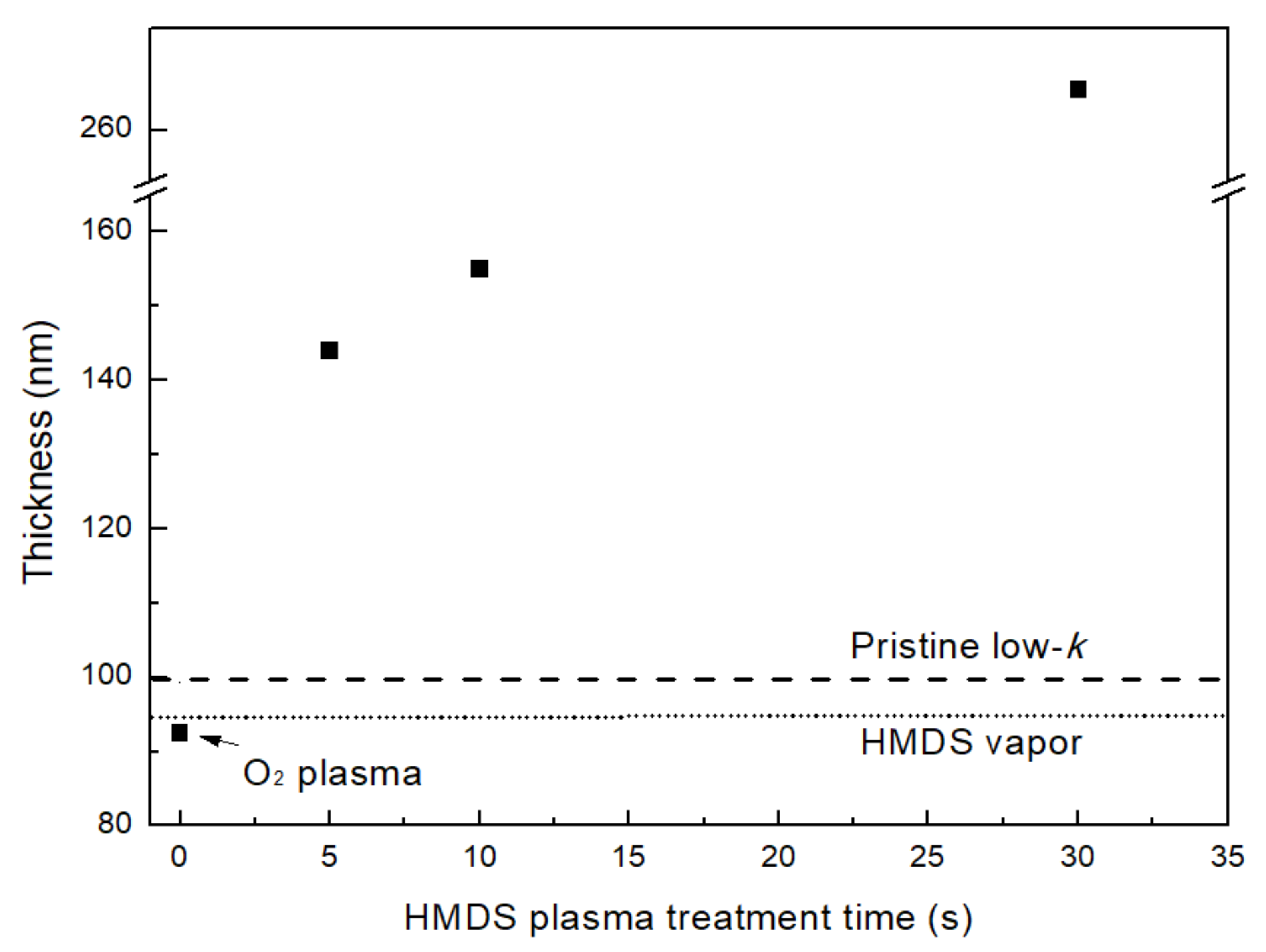
Figure 2 shows the change in the thickness of porous low-
k films due to HMDS treatment. The thickness of porous low-
k films slightly decreased after O
2 plasma treatment, representing the densification effect. The following HMDS treatment increased the thickness. In HMDS vapor treatment, a slight thickness increase with ~3 A was observed, being likely to form self-assembled monolayers (SAMs) on the film’s surface [
20]. It was observed that as the RF power was turned on for HDMS plasma treatment, the thickness increased with increasing plasma treatment time. During an irradiation in a plasma environment, HMDS precursor is decomposed to generate the reactive radicals by RF power. These radicals react and gradually form a dielectric layer on the surface of the porous low-
k film [
21].
Figure 3 exhibits the WCA values of porous low-
k films after O
2 plasma exposure and HMDS treatment. The reported WCA value was the average of five measurements. The measurement variation was within 1° for each condition. The WCA value of the as-deposited porous low-
k film was determined to be 85°, representing that the porous low-
k film tends to be hydrophobic. After O
2 plasma exposure, the WCA value decreased to 47°, indicating that the hydrophobic porous low-
k material was transformed to a hydrophilic film. A hydrophilic porous low-
k material tends to absorb more moisture from ambient air, thereby increasing the
k value and degrading dielectric reliability. The mechanism of hydrophilization transformation for the porous low-
k material upon O
2 plasma irradiation has been reported by many researchers [
22,
23,
24,
25]. Under an O
2 plasma environment, the generated reactive species (ions, radicals, and phonons) causes the breakage of Si–H and Si–CH
3 bonds, transforming to Si-O bonds and leaving many dangling bonds in the film. Some of those dangling bonds absorb moisture to form Si–OH bonds. These changes make a film to become a hydrophilic film. The subsequent HMDS vapor exposure recovered the WCA value back to 70°, suggesting that O
2 plasma-induced hydrophilic bonds are removed and are replaced by HMDS molecules by means of silylation mechanism [
16]. The following HMDS plasma treatment further increased WCA value. As HMDS plasma treatment time increased to 10 s, the WCA value reached saturation a value of 88°. Further increasing HMDS plasma treatment time did not change WCA value.
The mechanism of O
2 plasma irradiation and subsequent HMDS treatment on the porous low-
k film can be reflected by FT-IR spectra shown in
Figure 4. The main absorption peaks of the porous low-
k film are Si-O stretch network (1030 cm
−1), Si-O stretch cage-like peak (1120 cm
−1), Si-CH
3 stretch mode (1270 cm
−1), and Si-H stretch mode (2250 cm
−1) [
26,
27]. For the as-deposited porous low-
k film, peak at 3350 cm
−1 corresponding to Si-OH bonds was not detected, which is consistent with the WCA result. After O
2 plasma exposure, it can be found that the peak intensity of Si-O stretch network increased, indicating a more SiO
2-like character of the film. Additionally, the appearance of Si-OH bonds and the reduction of Si–CH
3 bonds were observed due to the conversion of the Si–CH
3 bonds into Si–OH bonds. The disappeared Si–CH
3 bonds appeared as the O
2 plasma-treated porous low-
k film was treated by HMDS vapor, representing that HMDS molecular helps to recover the hydrophobic Si-CH
3 bonds in the damaged film. The Si-OH bonds at 3350 cm
−1 was still observable in the HMDS-irradiated sample, although, its intensity obviously reduced. As the HMDS plasma treatment was subsequently carried out, Si-OH bonds at 3350 cm
−1 were completely removed.
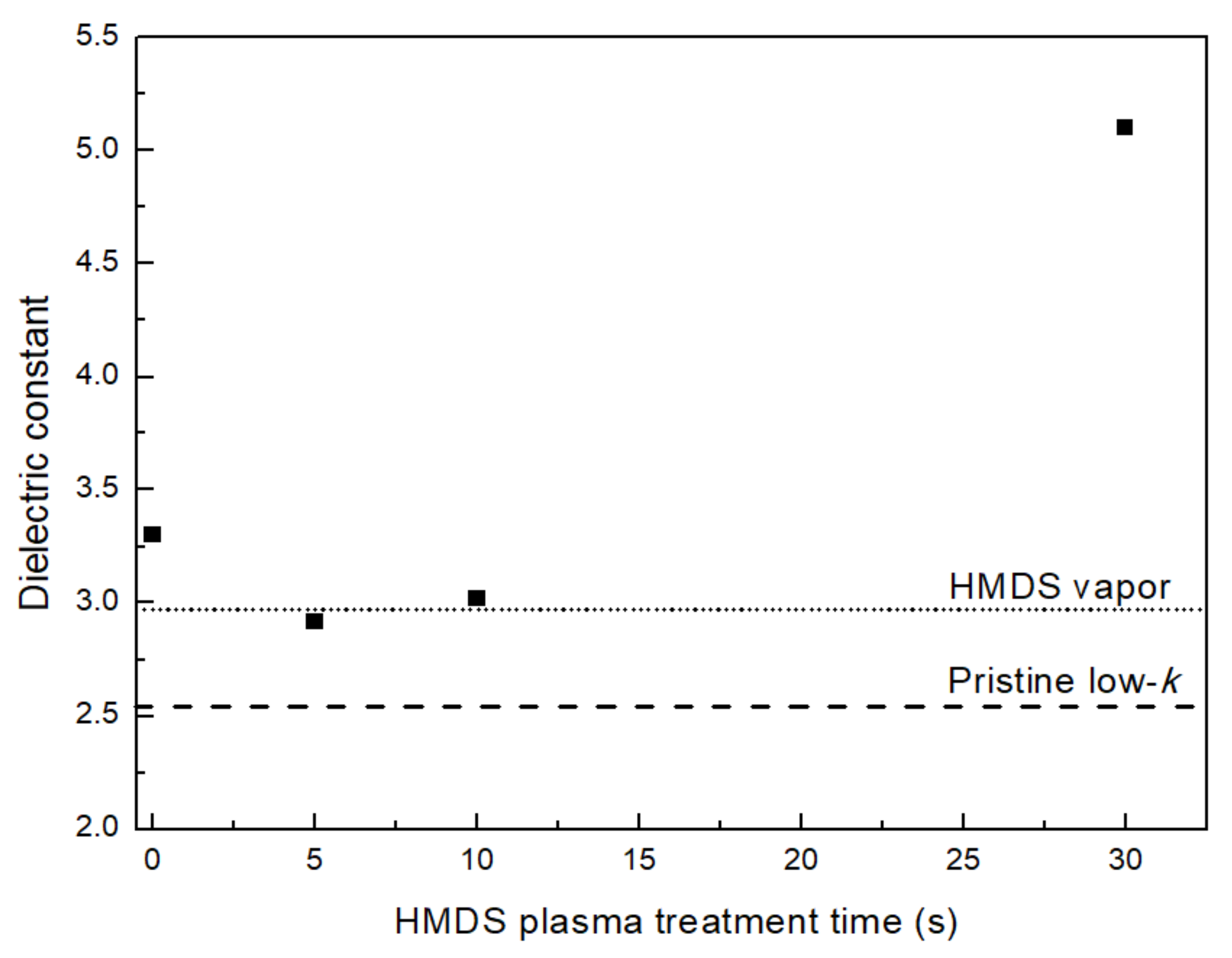
The increase in the
k value is the most concern issue for the integration of the porous low-
k material because it negatively impacts RC time delay. From
C-V measurements, the accumulation capacitance (
C) of MIS capacitors can be measured and the
k value of a dielectric film can be determined by using the expression of
k =
Cd/ε
0A. Here,
d is film thickness, ε
0 is absolute capacitivity in vacuum (8.85 × 10
−12 F/m), and
A is the area of the MIS capacitor.
Figure 5 shows the
k values of porous low-
k materials as a function of HMDS plasma treatment time. The results of O
2 plasma-irradiated and HMDS vapor-treated samples are also presented. As expected, O
2 plasma irradiation increased the capacitance, leading to an increased
k value with 3.36 for the porous low-
k material. The structural transformation with the depletion of Si-CH
3 bonds and the formation of Si-O and Si-OH bonds in the porous low-
k material upon O
2 plasma irradiation is responsible for the
k value increase. The O
2 plasma-treated sample was subsequent exposed to HMDS vapor, the measured capacitance decreased, thereby decreasing the
k value to 2.96. In the cases of following HMDS plasma treatment, the capacitance continuously reduced with time. However, the
k values were not expected to continuously decrease due to the formation of a dielectric layer onto the porous low-
k film. As HMDS plasma treatment time was 5 s, the overall
k value reduced to the minimum value of 2.92. Further increasing HMDS plasma time increased the
k value. This unique feature can be attributed to the competition of two mechanisms under HMDS plasma treatment: hydroxyl groups silylation and self-polymerization deposition. At the beginning of HMDS plasma treatment, silylation mechanism dominated, making hydroxyl groups in the O
2 plasma-treated porous low-
k film to be efficiently removed and silylated. With increasing HMDS plasma time longer than a critical time (5 s), HMDS self-polymerization deposition mechanism started to surpass silylation effect [
28]. As a result, a thick dielectric layer with a higher
k value is formed onto the porous low-
k film, thereby increasing the overall
k value.
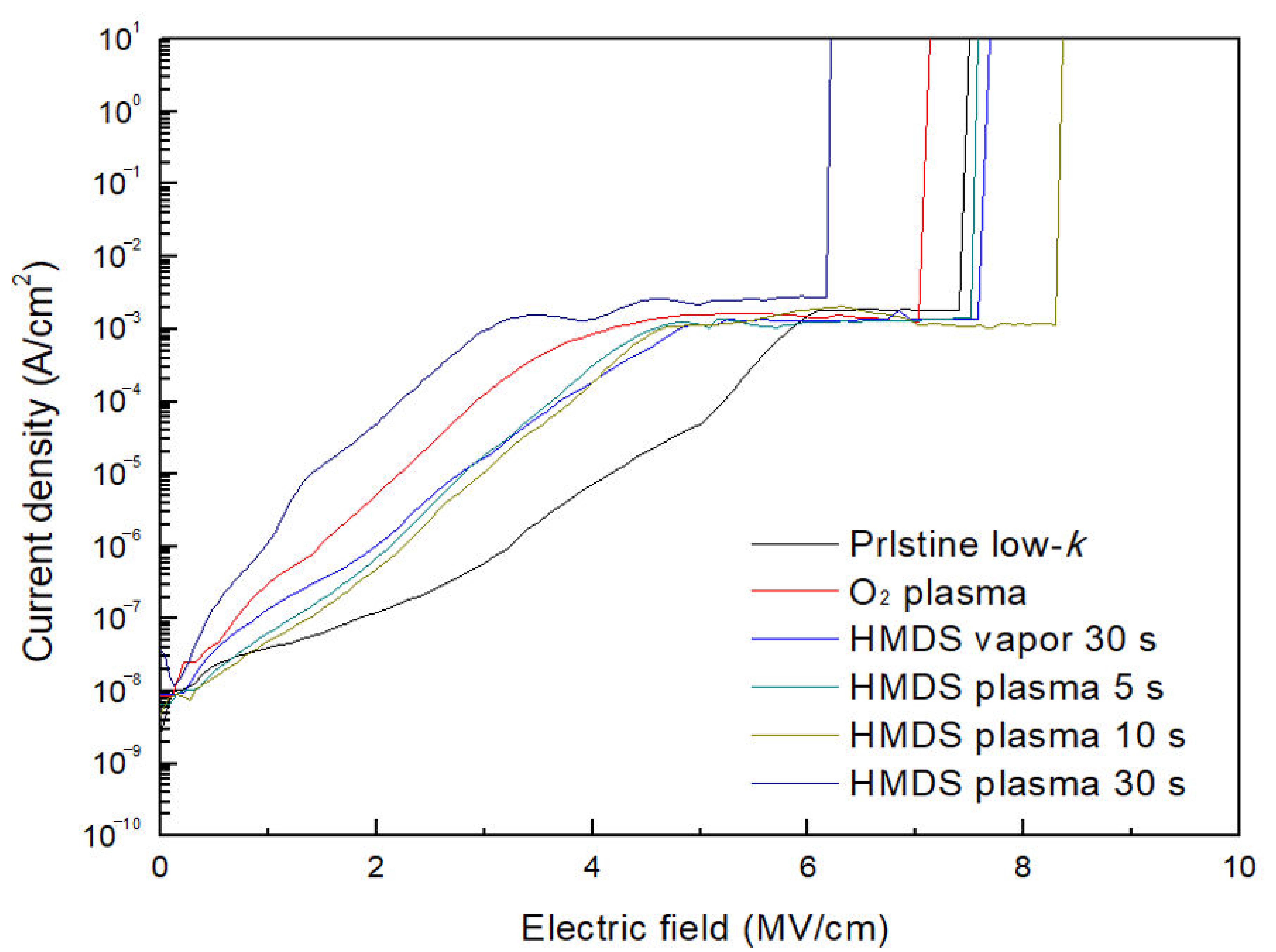
The leakage currents of the porous low-
k films after O
2 plasma irradiation and HMDS treatment were measured by sweeping the voltage until breakdown. The breakdown is defined as the monitored leakage current suddenly increases at least three-order of magnitude. The applied voltage was divided by the thickness of a dielectric film to transform to electric field (
E).
Figure 6 plots the measured
J-E curves of porous low-
k films with various treatments. Before breakdown, O
2 plasma-treated low-
k film had higher leakage currents than the pristine sample by two orders of magnitude. After HMDS treatment, the leakage current reduced, revealing that O
2 plasma-induced damage on the porous low-
k film can be repaired by HMDS treatment. However, the measured leakage currents were still higher than that of the pristine sample, suggesting that the repair effect due to HMDS treatment cannot reach the full recovery. As O
2 plasma-treated porous low-
k film was exposed to HMDS plasma with a treatment time of 10 s, its leakage current was observed to be the lowest.
The breakdown fields of the porous low-
k films with various treatments can be determined by the measured
I-E curves. Ten samples were measured for each condition and the average breakdown field was reported, as presented in
Figure 7. For the pristine porous low-
k film, its breakdown field was 7.54 MV/cm. As the porous low-
k film was irradiated by O
2 plasma, plasma-induced damage occurred, thereby reducing its breakdown field to 6.69 MV/cm. The subsequent HMDS vapor exposure and HMDS plasma treatment recovered the breakdown field for O
2 plasma-treated low-
k film. As HMDS plasma treatment time was 10 s, the breakdown field reached the maximum value of 8.32 MV/cm, which is higher than that of the pristine sample. This improvement can be attributed to the repair of O
2 plasma-induced damage and pore-sealing by capping a dielectric layer. As HMDS plasma treatment time further increased to 30 s, a very thick dielectric layer formed onto the porous low-
k film by HMDS self-polymerization reaction. Simultaneously, plasma-induced damage on the underlying porous low-
k film occurred, thus weakening the breakdown field of the stacked dielectric film.
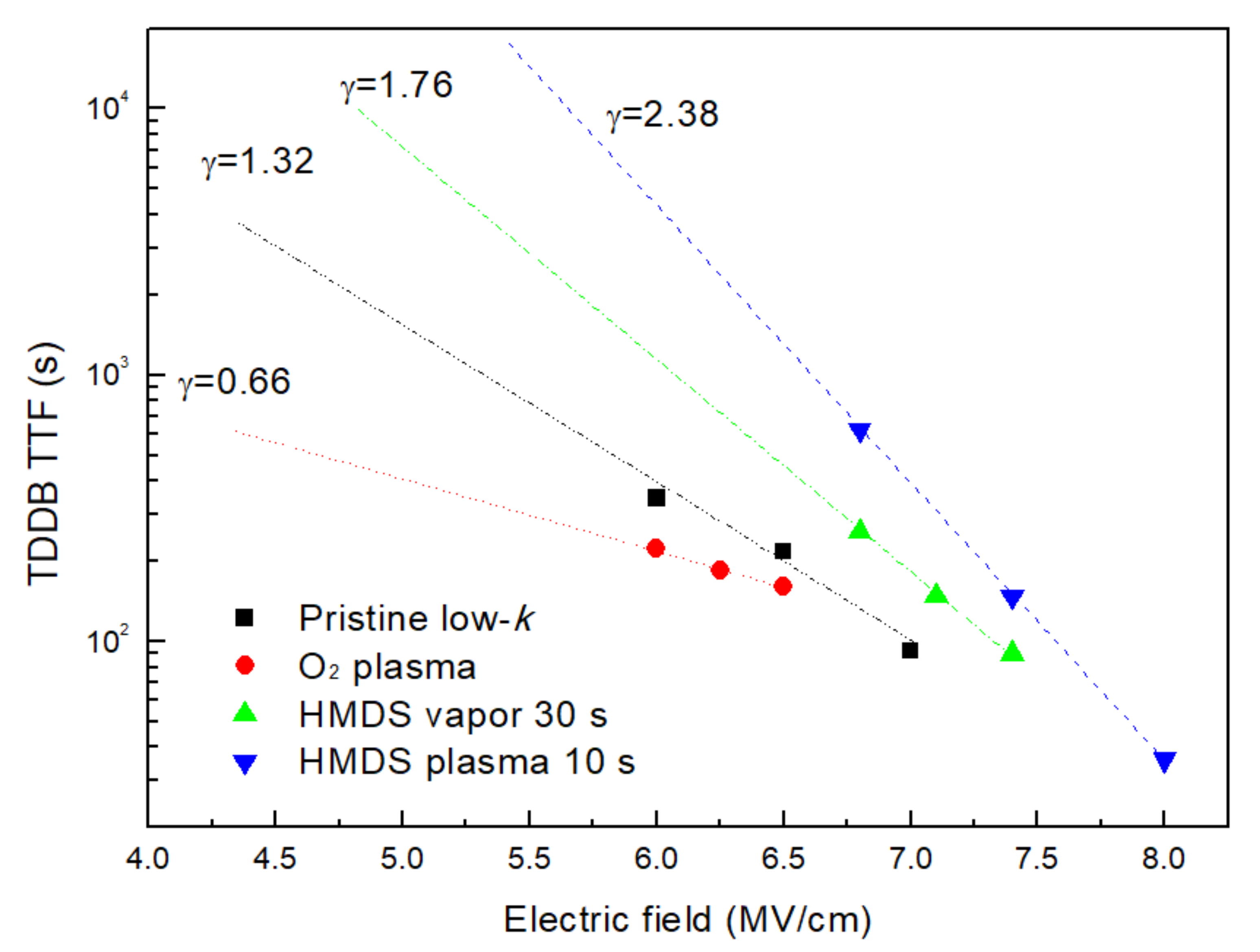
The long-term reliability of O
2 plasma-treated porous low-
k films before and after HMDS treatment was evaluated by TDDB tests. During a TDDB test, a constant field is continuously applied, and the leakage current is monitored until breakdown. The breakdown is defined as the monitored leakage current suddenly increases at least three-order of magnitude and the stressing time at breakdown is recorded as time-to-failure (TTF). Three stressing fields were used for each sample and ten MIS capacitors were measured for each condition.
Figure 8 plots the median TTFs of porous low-
k films with various treatments as a function of applied stressing field. For all tested samples, their TTFs decreased with increasing electric field, indicating that the dielectric breakdown is strongly controlled by the applied field. Moreover, the breakdown times of porous low-
k films were impacted by treatment processing. It is clearly observed that O
2 plasma-treated porous low-
k film had the worst TDDB TTFs. Under O
2 plasma exposure, defects were accumulated in the porous low-
k film, thereby accelerating breakdown during a TDDB test. The subsequent HMDS vapor and plasma treatments on O
2 plasma-treated low-
k films improved TDDB TTFs. The obtained TDDB TTFs were larger than those of the pristine sample. The improvement is attributed to not only plasma-induced damage repair but also surface pore-sealing due to HMDS treatment. The porosity in a low-
k film has been reported to significantly degrade reliability characteristics [
29]. As a result, pore-sealing processing is regarded as an important strategy to promote dielectric reliability for highly porous low-
k films. In this study, surface pores of the porous low-
k film were sealed by HMDS molecular during short-time HMDS vapor and plasma processing. SAMs were formed on the film’s surface, thereby retarding the formation of the connecting conductive path to trigger breakdown.
Furthermore, the E model (TTF∼exp(-γE)) was used to evaluate the impact of the applied field on TTFs for porous low-
k films that underwent various treatments. In the E model, the dielectric breakdown is dominated by the thermo-chemical bonding-breaking mechanism [
30,
31] and γ is a field acceleration factor. A higher γ value means a stronger field-dependence and can provide a longer lifetime in a lower operation field. The extracted γ values for porous low-
k dielectric films with various treatments are also listed in
Figure 8. For all studied samples, their TDDB TTFs were found to fit well with the E model, as confirmed by good correlation with the bonding-breaking mechanism. However, a slightly deviation from the E model was found in the O
2 plasma-treated porous low-
k film. Additionally, the O
2 plasma-treated sample had much lower TDDB TTFs and a smaller γ value. These features imply that O
2 plasma exposure is likely to produce an additional mechanism to accelerate dielectric failure for porous low-
k films. For the porous low-
k film underwent O
2 plasma exposure, carbon groups at its surface are removed and a weakened SiO
2-like layer is formed, capturing more moisture. These changes lower the energy barrier at the dielectric surface, enhancing TDDB degradation [
32]. As the O
2 plasma-treated porous low-
k film was subsequently exposed to HMDS vapor, absorbed moisture was partially removed and partial carbon groups at the surface were recovered. The recovery characteristics help to increase TDDB TTFs and γ value. Further HMDS plasma treatment with a treatment time of 10 s enhanced TDDB TTFs and γ value, attributing to mechanisms of moisture removal off, pore-sealing, and dielectric layer capping.
A dielectric layer was formed onto the surface of the porous low-
k film due to HMDS treatment and its Cu barrier capability was evaluated by applying a positively biased electric stress using Cu-gate MIS capacitors. After electric stress,
C-V curves were measured, and the flat-band voltage (V
fb) was determined.
Figure 9 plots the V
fb shifts with stressing time for porous low-
k films with various treatments. The applied field was fixed at 5 MV/cm with different intervals. For the pristine porous low-
k film after electric stress, V
fb shifted to the negative voltage and the shifting magnitude amplified with stressing time. Negative voltage shift of V
fb is reportedly attributed at the trapping of positively charged ions [
33]. In the used Cu-gate MIS capacitors in this study, the introduced positively charged ions into the porous low-
k film under positively-biased electric stress are most likely to be Cu ions. This result again illustrates that a barrier is required for porous low-
k films. As shown in
Figure 9, O
2 plasma-treated sample displayed a different V
fb shift direction. Its positive V
fb shift represents that the drift of Cu ions under electric stress are effectively suppressed due to the formation of the densification layer on the film’s surface. On the other hand, the positive V
fb shift indicated that the negatively charged electrons are trapped in the O
2 plasma-treated low-
k film. As O
2 plasma-treated samples were subsequently treated by HMDS vapor and plasma, V
fb shifted toward the negative voltage after electric stress, but the shifting magnitude was lower than that of the pristine sample, indicating that the formation layer by HMDS treatment can block the drift of Cu ions. As the sample was further irradiated by HMDS plasma, negligible V
fb shift was detected after electric stress, revealing that barrier capacity against Cu migration is enhanced. The result concludes that a dielectric layer formed by HMDS plasma treatment is a superior Cu barrier for the porous low-
k dielectric film.
