Article

Laser-Induced Thermal Stresses in Dense and Porous Silicon Dioxide Films

by
Fedor Vasilievich Grigoriev
1,2,*,
Vladimir Borisovich Sulimov
1,2 and
Alexander Vladimirovich Tikhonravov
1,2
1
Research Computing Center, M.V. Lomonosov Moscow State University, Leninskie Gory, Moscow 119234, Russia
2
Moscow Center for Fundamental and Applied Mathematics, M.V. Lomonosov Moscow State University, Leninskie Gory, Moscow 119234, Russia
*
Author to whom correspondence should be addressed.
Coatings 2021, 11(4), 394; https://doi.org/10.3390/coatings11040394
Submission received: 26 February 2021 / Revised: 19 March 2021 / Accepted: 24 March 2021 / Published: 30 March 2021
(This article belongs to the Special Issue Glancing Angle Deposited and Anisotropic Thin Films and Coatings)

Abstract

:
The laser-induced thermal stresses in silicon dioxide films are calculated using molecular dynamics simulations. The absorption of the laser energy is simulated by the linear temperature growth from room temperature to 1300 K in a time equal to the laser pulse duration. The maximum values of stresses for picosecond pulses are approximately twice as high as for nanosecond pulses. The stresses in highly porous glancing angle deposited films are approximately two times lower than in dense films. Stress waves caused by picosecond pulses are observed in dense films. An increase in the heating temperature to 1700 K leads to an increase in the absolute stress values for picosecond pulses, and a decrease for nanosecond pulses.

Graphical Abstract

1. Introduction

The investigation of the possible causes of laser-induced damage to optical films is an important task in many applications of high-power lasers [1]. To date, there is still no complete understanding of the effects resulting in laser-induced damage to transparent dielectric coatings. Thermoelastic breakdown, caused by thermal expansion and the associated stresses, is considered as one of such effects [2].
Laser-induced thermal stresses have been investigated in different coatings, both experimentally and theoretically. The propagation of laser-induced elastic waves in fused silica and a single Si crystal was experimentally studied in [3]. It was found that the maximum stress is observed at the interface between the film and the substrate. The interface stress increases with increasing film thickness and decreases with increasing substrate thickness. The surface acoustic waves arising from the laser energy absorption in the thin film–substrate system were investigated both experimentally and theoretically in [4]. Wave-induced stresses were calculated using a finite element model. The dependence of the interfacial stresses on the ratio of the wavelength-to-film thickness was investigated. The correlation between the polarization state of the femtosecond laser radiation and the anisotropy of stresses arising in films during laser writing was experimentally investigated in [5]. Based on the volume expansion model, the maximum stress in fused silica was calculated as 2 GPa [5].
In Ref. [6], the finite element model was developed to simulate laser-induced stress waves in dielectric multilayer coatings. The model allows the study of the dependence of the degradation of material structural integrity, caused by stress waves, on the coating’s geometric and material parameters. It was found that closer impedance of the materials of the layers decreases interface stresses by 20%–30%. Also, increasing the thickness of a single layer reduces the maximum interfacial stress. In Ref. [7], the heat conduction and elastic equations were solved in the case of a single Gaussian laser pulse absorbed by the MgF2/ZnS double layer. The distributions of the temperature and stresses over the film thickness were calculated. The factors influencing these distributions were identified and discussed. In Ref. [8], the 2D finite element model was used to simulate the laser-induced thermal stresses in different optical thin-film materials. It was found that for all the materials, the induced stress is compressive. The smallest absolute value of stresses was obtained for the MgF2 film.
Compared with the finite element models, the atomistic simulation methods allow the study of the processes of laser energy absorption at the microscopic level. This is especially important when simulating the fast processes with times in the order of picoseconds or less. The stresses in nickel films, caused by femtosecond laser pulses, were studied using molecular dynamics (MD) simulations in Ref. [9]. It was found that ultrafast heating results in the formation of a 100 nm thick strongly compressed layer below the film surface. This layer remains compressed for less than 50 ps. The laser pulses with low intensity form only a single elastic wave.
The MD method was applied in [10] to study the stresses in growing silicon dioxide films. The stresses were calculated for dense films and for glancing angle deposited (GLAD) films. It was found that the absolute values of stresses in GLAD films are several times less than in dense films. Also, for GLAD films, stress anisotropy in the substrate plane was found.
In this work, the earlier developed MD-based method [11,12,13] was modified and applied to simulate laser-induced thermal stresses in dense and GLAD silicon dioxide films. Laser pulses of different durations were considered. The dependence of the stress values on the thin films structure and on the heating temperature is discussed.

2. Method

The simulation scheme is shown in Figure 1. The atomistic cluster represents the part of the film and substrate exposed to laser irradiation (bottom of Figure 1). To calculate the laser-induced thermal stresses, the following steps are performed:
  • Simulation of the deposition of SiO2 thin films as described in the section below.
  • Equilibration of the deposited structure in the NPT (constant number of particles, pressure and temperature) ensemble. The asymmetric barostat is applied to ensure independent variation in the cluster dimensions during equilibration. This step is necessary to eliminate stresses that appear during thin-film deposition;
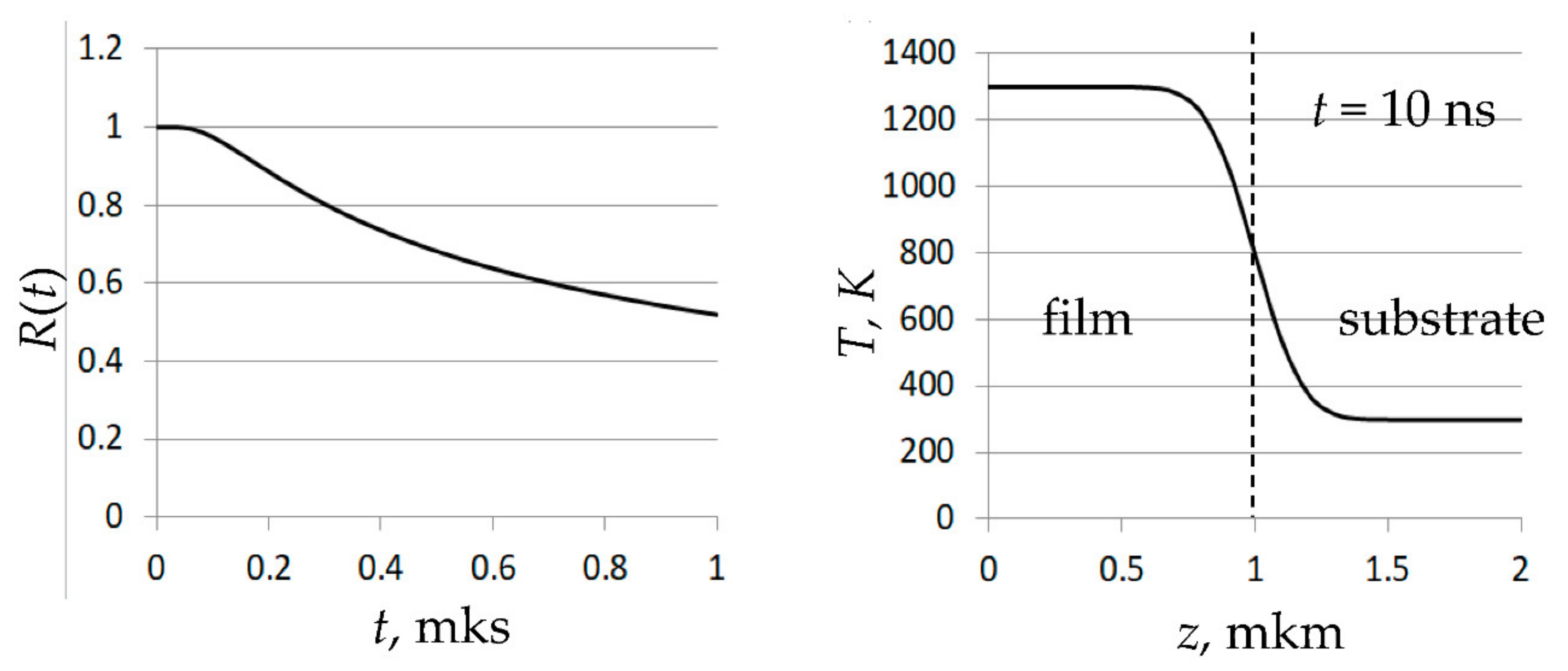
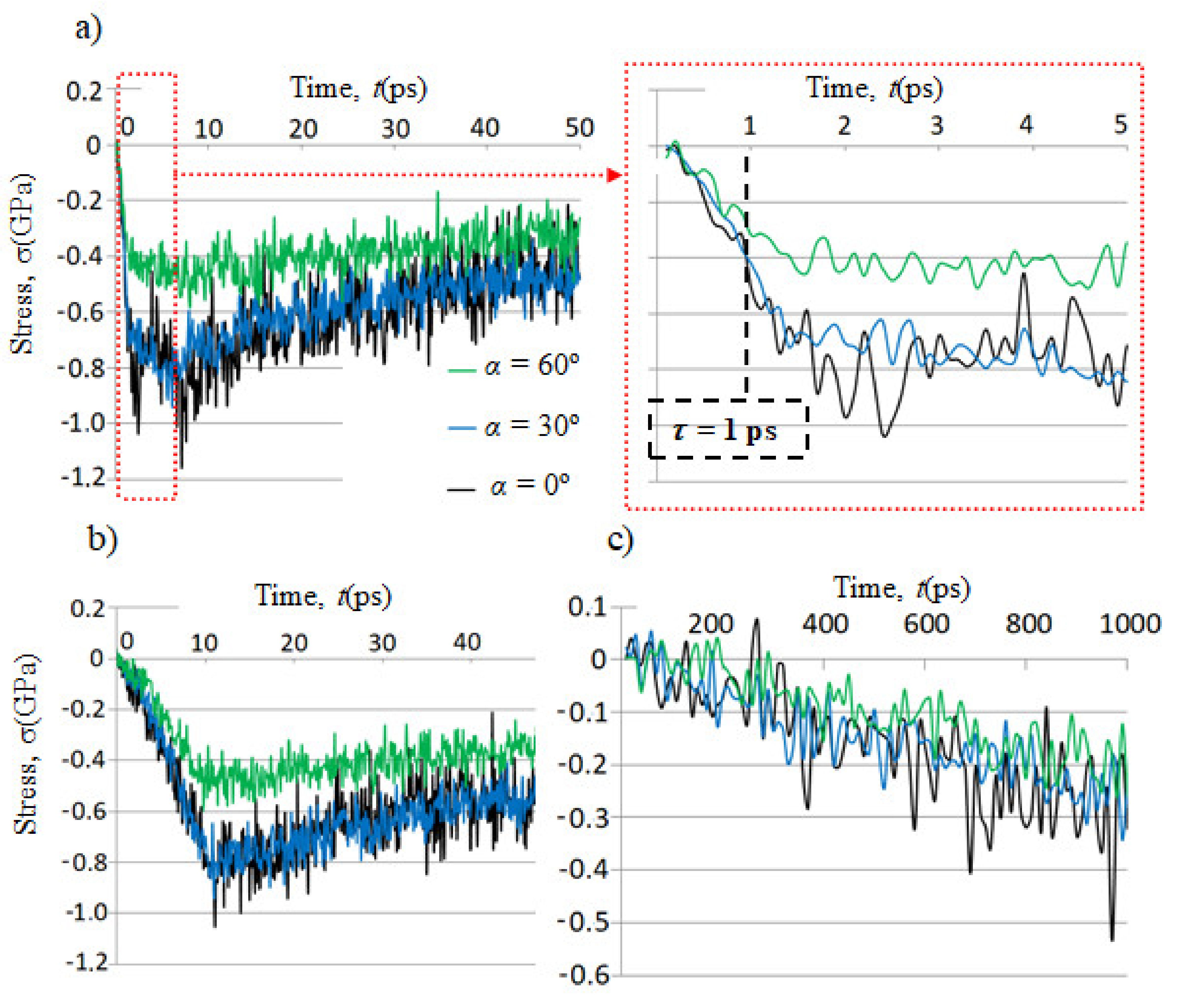
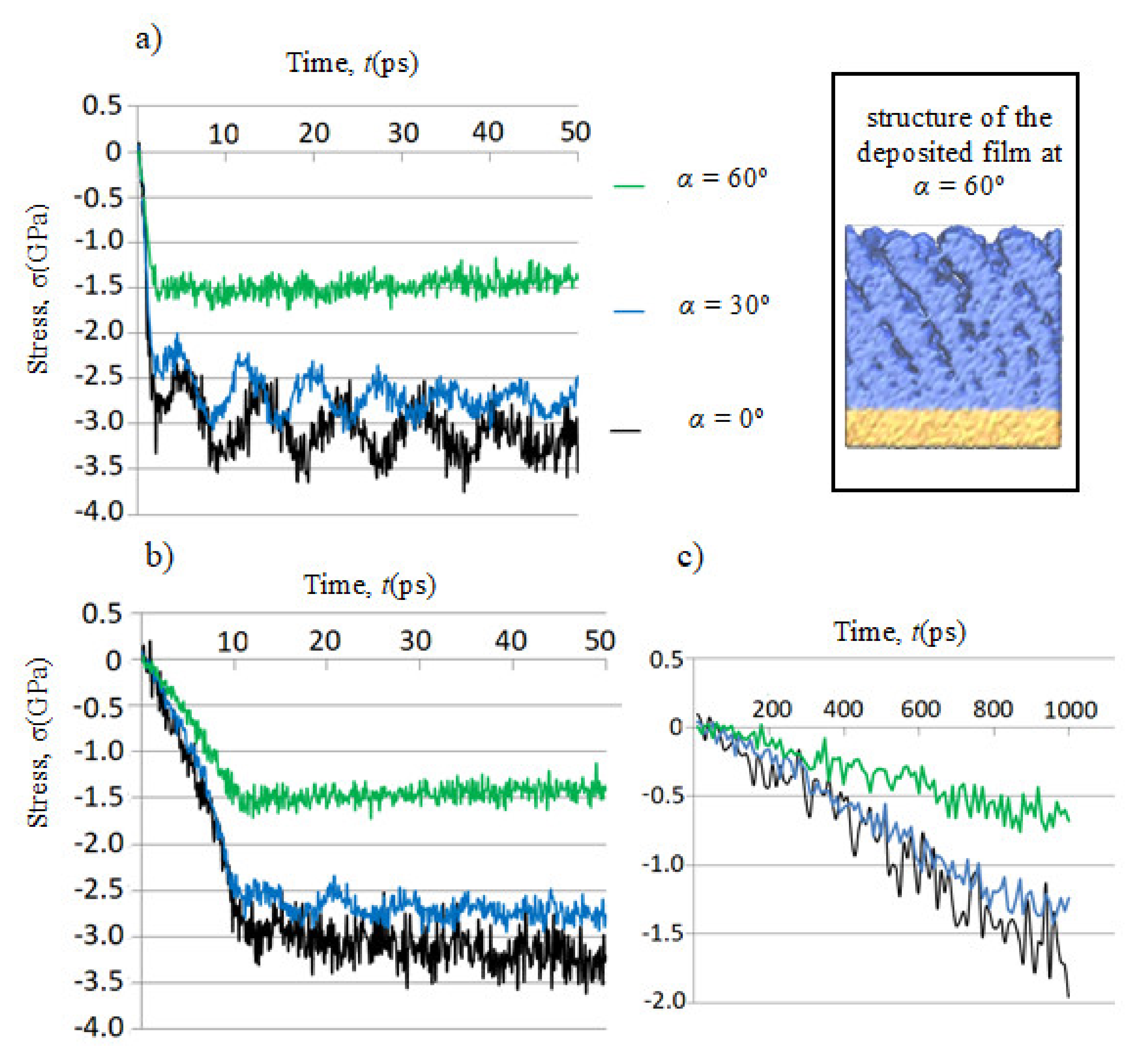
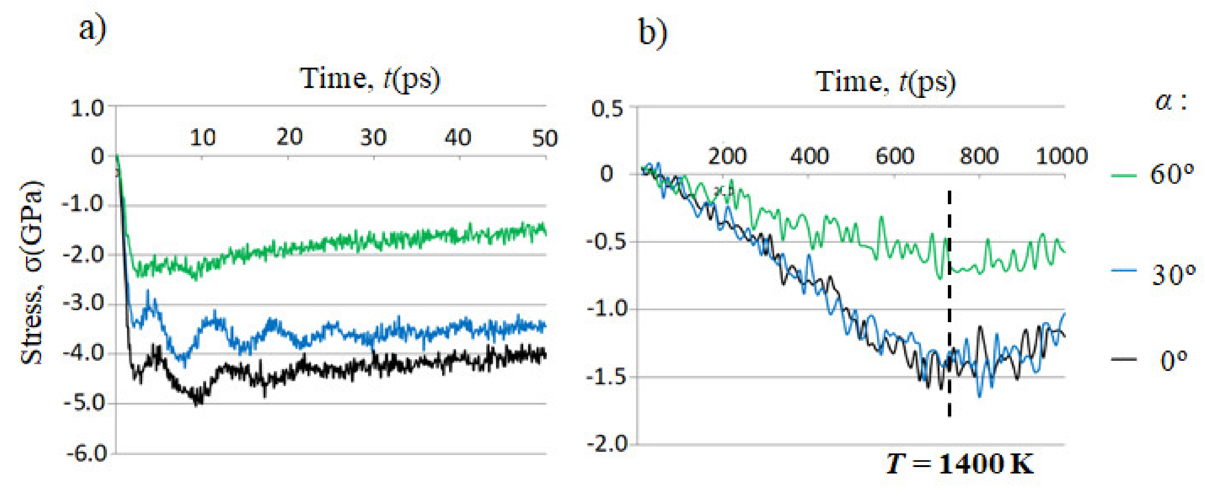
  • Modeling the absorption of laser radiation in the film by increasing the cluster temperature to the value Tf. The heating is assumed to be uniform over the film volume since the cluster thickness of 40 nm is insufficient to consider the distribution of the laser radiation intensity along the z-axis inside the film. The calculations of stresses are averaged over the film volume during the film heating;
  • In the case of the fast laser pulses with durations of τ = 1 ps and τ = 10 ps, the stresses are also calculated during the relaxation time τr after the end of the film heating. The temperature during this period is kept equal to Tf.
The laser-induced thermal stress is studied using the atomistic clusters of the silicon dioxide films obtained in our previous work [10,12,13]. These clusters were deposited using the MD-based step-by-step scheme [11]. Oxygen and silicon atoms are randomly inserted into the upper part of the modeling box in a stoichiometric proportion of 1:2. The initial velocities are directed to the substrate. The values of the velocities correspond to the energies E(Si) = 10 eV and E(Si) = 0.1 eV for high- and low-energy deposition processes, respectively, and E(O) = 0.1 eV in both cases. Then the MD simulation starts in the NVT (constant number of particles, volume and temperature) ensemble. The periodic boundary conditions are applied. The duration of one injection step is equal to 10 ps, and one time step is equal to 0.5 fs. The horizontal substrate dimensions are equal to 10 nm and 30 nm. The substrate thickness in a vertical direction is equal to 6 nm. The thicknesses of the deposited films are about 40 nm. The temperature of the simulation cluster is kept equal to 300 K using the Berendsen thermostat [14]. The energy of the interatomic interactions is calculated using the empirical pairwise DESIL (DEposition of SILica) force field [11]. The deposition is performed at different values of the deposition angle α (Figure 1).
The stress tensor σ is calculated as follows [10,15,16]:
σ = 2 V K Ξ
where V is the modeling box volume, K is the kinetic energy tensor, Ξ is the virial tensor.
K = 1 2 i = 1 N m i υ i υ i ; Ξ = 1 2 i , j = 1 , i j N f i j r i j
where ⊗ is the direct product of two vectors, mi and υ i are the atomic masses and velocities, r i j is the radius vector directed from the i-th atom to the j-th atom, f i j is the force acting from the i-th atom to the j-th atom, and N is the number of atoms.
MD simulations are performed using the GROMACS package, ver. 5.1.1 [15]. The Visual Molecular Dynamics (VMD) package, ver. 1.9.3 is used for visual analysis [17]. The simulation is carried out using equipment at the shared research facilities of high-performance computing resources at Lomonosov Moscow State University [18].

3. Results and Discussion

In this work, we investigated the stresses induced by heating to the temperature Tf below the softening point of fused silica, 2.0 × 10³ K [19]. The results of the stresses calculation for low-energy-deposited SiO2 films are presented in Figure 2. Hereinafter, σ = (σxx + σyy)/2, where σxx and σyy are the diagonal components of the stress tensor, Equation (1), and the axes directions are shown in Figure 1. The fast oscillation of σ is due to a limited number of particles in the simulation clusters which leads to noticeable thermodynamic fluctuations of the calculated stresses. (see Appendix A).
The temperature of the films increases linearly from an initial temperature of 300 K to Tf = 1300 K. We assume that the temperature of 1300 K corresponds to the value of the laser intensity, which is not much lower than the laser-induced damage threshold for SiO2 films, ~4 J/cm2 [20].
The heating time is denoted as τ and is taken to be 1 ps, 10 ps, and 1 ns, which corresponds to the picosecond and nanosecond laser pulses. The plots in Figure 2 show the stress values averaged over segments of the MD trajectories, with a duration of 0.1 ps.
After the end of heating, the film temperature begins to decrease. To estimate the characteristic time of this decrease, the heat conduction equation is solved for the model task on the condition that there is uniform absorption in the film, with realistic thicknesses of the film and the substrate. It is found that the temperature of the upper edge of the film, deposited on a 1 mm thick substrate, decreases by less than one percent of the maximum value during several microseconds. Increasing the substrate thickness increases the temperature-reducing time. In all the cases, this time is much longer than the times of the MD simulations. For this reason, the temperature is kept equal to Tf during the simulation, after the end of the heating.
In all the cases, the sign of the stresses is negative, which corresponds to the compressive stress. In the case of τ = 1 ps, the stress grows for approximately 1–2 ps after the end of heating (see the enlarged plots inside the red rectangle at the top of Figure 2). The stress values change insignificantly when the time of heating increases from τ = 1 ps to τ = 10 ps (compare Figure 2a,b). However, when the time of heating increases to 1 ns, the stress reduces approximately twice (Figure 2c). This could be attributed to the fact that the structure has more time for relaxation under nanosecond heating.
The maximum stress values significantly decrease with an increase in the deposition angle from α = 30° to α = 60°. This is due to the fact that deposition of the large angle results in the formation of the glancing angle deposited (GLAD) films with high porosity [21]. The densities of the SiO2 films for various deposition angles and various deposition energies are shown in Table 1. The density changes insignificantly with an increase in the deposition angle from α = 0° to α = 30°, while a further increase in α to 60° leads to a noticeable decrease in density. The stresses demonstrate a similar dependence on α (Figure 2).
As mentioned in the Section 1, laser-induced stresses can cause thermoelastic breakdown of the coatings structure. Thus, a decrease in stresses with an increase in the deposition angle can be accompanied by an increase in the laser-induced damage threshold (LIDT). Indeed, in [22] the increase in the LIDT of silicon dioxide films with growth of the deposition angle has been observed experimentally.
The results of the stress calculation for high-energy-deposited silicon dioxide films are shown in Figure 3. The absolute values of the stresses are several times higher than for the low-energy-deposited films (Figure 2). This can be explained by a decrease in the film porosity with an increase in the deposition energy. Indeed, even for α = 60° the density of the high-energy-deposited film is higher than the density of the low-energy film deposited at α = 0° (Table 1). Accordingly, the absolute stress values in all high-energy-deposited films are higher than in low-energy-deposited films. In the GLAD film (α = 60°), the stresses are approximately half that of the normally deposited film (α = 0°). The formation of film layers, with a high value of compress stress under laser irradiation, was demonstrated earlier in the MD simulations [9].
With fast heating (Figure 3a), periodic changes in stress values are observed in the cases of α = 0° and α = 30°. The period of these changes is about 10 ps. We assume that these changes indicate the appearance of stress waves caused by fast heating. Assuming that the wavelength of such waves is close to the characteristic dimension of the simulation area, we find that the wave velocity is about a few km/s. This corresponds to the sound velocity in solids. It can be seen, from the plots in Figure 2 and Figure 3, that the stress waves are formed only in the case of picosecond heating of dense films. The slight difference in the periods at α = 0° and α = 30° can be caused by the difference in the film density, since the sound velocity depends on it. As mentioned in the Section 1, the thermally induced elastic waves were observed experimentally [3,4]. These waves can significantly affect the LIDT since their propagation leads to the spalling of thin-surface films [4]. Thus, the LIDT value of GLAD SiO2 films can be higher due to the absence of stress waves.
An increase in the heating temperature to Tf = 1700 K leads to an increase in the absolute values of thermal-induced stresses in high-energy-deposited films in the case of fast heating (Figure 4a). Stress waves are also observed in this case, but they decay within 20–30 ps after the end of heating. Apparently, this is due to the beginning of the softening of the structure upon heating to 1700 K. This softening prevents the propagation of elastic waves.
In contrast to fast heating, in the case of τ = 1 ns, an increase in the heat temperature Tf from 1300 K (Figure 3c) to 1700 K (Figure 4b) leads to a reduction in the absolute stress value. Moreover, a stress value reaches its maximum when the structure temperature is about 1400 K. A further increase in the temperature to 1700 K leads to a decrease in the stress values. We assume that this effect is also related to structure softening.
The calculated values of the stresses are in the interval of the experimental data. The stresses during the laser writing process in silica achieve 2 GPa [5]. The laser-induced compressive stress in silicon dioxide films, deposited by ion beam sputtering, achieve 1.6 GPa in the normal conditions of radiation at 1064 nm wavelength and a pulse duration of 5 ns [23]. The intensity of the laser irradiation in [24] is a laser-induced damage threshold of about 25 J/cm2. In [24] it was found that the stresses in SiO2/HfO2 multilayers achieve 5 GPa during the laser-induced damage process.
It is interesting to compare the values of thermal-induced stresses and stresses arising during the growth of silicon dioxide films, calculated for high-energy deposition [10]. The stresses in both cases are compressive. However, the maximum absolute values of thermal-induced stresses are several times higher than the stresses in growing films. In both cases, stresses vary insignificantly with increasing the deposition angle α from 0° to 30°. When the deposition angle increases from 30° to 60°, the relative reduction in stresses in the growing films is greater than the relative reduction in thermally induced stresses. Finally, the thermally induced stresses at the considered heating temperature are noticeably higher than the stresses in the growing film. On the other hand, the thermal stresses, in contrast to the stresses arising during the film’s deposition, affect the film only for a limited time.

4. Conclusions

The laser-induced stresses in dense and porous silicon dioxide films are calculated using MD simulations. The absorption of the laser energy is simulated by the linear temperature growth from room temperature to a final temperature of 1300 K and 1700 K in a time equal to the laser pulse duration. The stresses in high-energy-deposited films are approximately two times higher than in low-energy-deposited films. This difference is caused by the low porosity of the low-energy-deposited films. At a given deposition energy, the stresses in the GLAD films are less than the stresses in normally deposited films. This result agrees with the experimental data.
The picosecond laser pulses produce stress waves in the high-energy-deposited dense films. These waves are not observed in low-energy-deposited films or in high-energy GLAD films. Stress waves can significantly affect LIDT as they lead to spalling of thin-surface films.
For high-energy-deposited films, an increase in the heating temperature to 1700 K leads to an increase in the absolute stress values in the case of picosecond pulses, and to a decrease in these values in the case of nanosecond pulses. We assume that the latter effect is caused by the softening of the films structure, since the temperature of 1700 K is close to the experimentally known softening temperature of fused silica, 2 × 10³ K.

Author Contributions

Сonceptualization, A.V.T., F.V.G., V.B.S.; methodology, F.V.G.; software, F.V.G. and V.B.S.; validation, F.V.G.; formal analysis, F.V.G.; investigation, F.V.G.; resources, A.V.T. and V.B.S.; data curation, A.V.T. and V.B.S.; writing—original draft preparation, F.V.G.; writing—review and editing, A.V.T. and V.B.S.; visualization, F.V.G.; supervision, A.V.T. and V.B.S.; project administration, V.B.S.; funding acquisition, A.V.T. and V.B.S. All authors have read and agreed to the published version of the manuscript.

Funding

The work is supported by the Russian Ministry of Science and Higher Education, agreement no. 075-15-2019-1621.

Institutional Review Board Statement

Not applicable.

Informed Consent Statement

Not applicable.

Data Availability Statement

Data sharing is not applicable.

Conflicts of Interest

The authors declare no conflict of interest.

Abbreviations

GLADglancing angle deposition;
MDmolecular dynamics;
NPTconstant number of particles, pressure and temperature;
NVTconstant number of particles, volume and temperature;
LIDTlaser induced damage threshold. All other abbreviations refer to program names;
DESILDEposition of SILica;
VMDVisual Molecular Dynamics.

Appendix A

The characteristic time of the temperature decrease can be calculated using the heat conduction equation, as follows:
T z , t t a 2 2 T z , t z 2 = I z
where a2 = χ/(сρ), с, χ and ρ are the specific heat capacity, heat conductivity and mass density, respectively, I(z) is the function proportional to the absorbed energy. The direction of the z-axis is shown in Figure A1. The film and substrate thickness are denoted as d and L, respectively (Figure A1). The following boundary and initial conditions are applied:
T z , t z z = 0 = 0
T L , t = T 0
T z , 0 = T 0
It is assumed in Equation (A3) that the temperature of the lower edge of the substrate is kept equal to the initial temperature before heating. At the initial moment, the film starts to absorb energy according to the uniform distribution function (Figure A1).
Figure A1. Function, describing the energy absorption.
Coatings 11 00394 g0a1
The solution of Equation (A1) is given by the following function:
T z , t = T 0 + n = 0 d n α n 1 exp α n t cos λ n z )
where:
d n = 2 L 0 d I cos λ n z d z = 2 I sin λ n d λ n L ; λ n = 𝜋 1 2 + n L ;     n =   a 2 λ n 2
At the end of absorption, the temperature distribution T 1 z , t is found as the solution of the heat equation with the following conditions:
T 1 z , t   t a 2 2 T 1 z , t   z 2 = 0
T 1 z , t z z = 0 = 0
T 1 z , t = T 0
T 1 z , 0 = T z , 𝜏 ,
where τ is the laser pulse duration, T z , 𝜏 is given by Equation (A5). The solution of Equation (A7) is given by the following function:
T 1 z , t = T 0 + n = 0 d n n 1 exp α n 𝜏 cos λ n z exp α n t
The relative reduction in the temperature at the upper edge of the film (z = 0) can be characterized by the following function:
R t = T 1 0 , t T 0 T 1 0 , 0 T 0 = n = 0 d n n 1 exp α n 𝜏 exp α n t n = 0 d n n 1 exp α n 𝜏
The material parameters are с = 103 J/(kg·К), ρ = 2.2 × 10³ kg/m3, and χ = 2.0 W/(m·К) [25].
The graph of the function R(t) is shown on the left side of Figure A2. The substrate thickness is L = 1 mm, the film thickness is d = 1 mkm, which corresponds to the technological dimensions. As can be seen from the plot, the temperature of the upper edge of the film changes insignificantly during the first several tens of nanoseconds. This means that in the MD simulation with nanoseconds trajectories, the temperature after the end of heating is practically constant. If the substrate thickness exceeds 1 mm, then the temperature decreases slower than in the considered case.
The dependence of the temperature on the vertical coordinate is shown on the right in Figure A2. As can be seen, 10 ns after the end of heating, the temperature inside the film layer with z < 0.5 mkm is practically constant. So, the temperature inside the 40 nm thick layer can also be considered as constant during the simulation time of 1 ns or less.
Figure A2. Dependence of R(t), Equation (A12), versus time t after the end of film heating, and the dependence of the film temperature T, Equation (A11), along the vertical coordinate z (see Figure 1) at moment t = 10 ns after the end of film heating.
Coatings 11 00394 g0a2

References

  1. Manenkov, A.A. Fundamental mechanisms of laser-induced damage in optical materials: today’s state of understanding and problems. Opt. Eng. 2014, 53, e010901. [Google Scholar] [CrossRef]
  2. Feit, M.D.; Campbell, J.H.; Faux, D.R.; Genin, F.Y.; Kozlowski, M.R.; Rubenchik, A.M.; Riddle, R.A.; Salleo, A.; Yoshiyama, J.M. Modeling of laser-induced surface cracks in silica at 355 nm. Laser-Induc. Damage Opt. Mater. 1997 1998, 3244, 350–355. [Google Scholar] [CrossRef] [Green Version]
  3. Wang, J.; Weaver, R.L.; Sottos, N.R. A parametric study of laser induced thin film spallation. Exp. Mech. 2002, 42, 74–83. [Google Scholar] [CrossRef]
  4. Sherman, B.; Liou, H.-C.; Balogun, O. Thin film interface stresses produced by high amplitude laser generated surface acoustic waves. J. Appl. Phys. 2015, 118, 135303. [Google Scholar] [CrossRef]
  5. Ben McMillen, B.; Bellouard, Y.Y. On the anisotropy of stress-distribution induced in glasses and crystals by non-ablative femtosecond laser exposure. Opt. Express 2015, 23, 86–100. [Google Scholar] [CrossRef] [PubMed] [Green Version]
  6. Gracewski, S.M.; Boylan, S.; Lambropoulos, J.C.; Oliver, J.B.; Kessler, T.J.; Demos, S.G. Simulation of internal stress waves generated by laser-induced damage in multilayer dielectric gratings. Opt. Express 2018, 26, 18412–18422. [Google Scholar] [CrossRef] [PubMed]
  7. Cao, Q.; Su, J. Study on thermal effect and thermal stress effect of multilayer thin films induced by pulsed laser. In Proceedings of the Pacific Rim Laser Damage 2019: Optical Materials for High-Power Lasers, Qingdao, China, 8 July 2019. [Google Scholar]
  8. Firth, A.; Srinivasan, U. Laser Induced Thermal Stress in Optical Thin Films. In Proceedings of the Optical Interference Coatings Conference (OIC) 2019: OSA Technical Digest, Santa Ana PuebloNM, USA, 2–7 June 2019. [Google Scholar] [CrossRef]
  9. Demaske, B.J.; Zhakhovsky, V.V.; Inogamov, N.; White, C.T.; Oleynik, I.I. MD Simulations of Laser-Induced Ultrashort Shock Waves in Nickel. In Proceedings of the Conference of the American Physical Society Topical Group on Shock Compression of Condensed Matter, Chicago, IL, USA, 26 June–1 July 2011; AIP Publishing: Melville, NY, USA, 2012; pp. 1163–1166. [Google Scholar] [CrossRef] [Green Version]
  10. Grigoriev, F.V.; Sulimov, V.B.; Tikhonravov, A.V. Atomistic Simulation of Stresses in Growing Silicon Dioxide Films. Coatings 2020, 10, 220. [Google Scholar] [CrossRef] [Green Version]
  11. Grigoriev, F.V.; Sulimov, A.V.; Kochikov, I.V.; Kondakova, O.A.; Sulimov, V.B.; Tikhonravov, A.V. Supercomputer modeling of the ion beam sputtering process: Full-atomistic level. In Proceedings of the Optical Systems Design 2015: Advances in Optical Thin Films V, International Society for Optics and Photonics, Bellingham, WA, USA, 7–10 September 2015; Volume 9627, p. 962708. [Google Scholar] [CrossRef]
  12. Grigoriev, F.; Sulimov, V.; Tikhonravov, A. Atomistic simulation of the glancing angle deposition of SiO2 thin films. J. Non-Cryst. Solids 2019, 512, 98–102. [Google Scholar] [CrossRef]
  13. Grigoriev, F.; Sulimov, V.; Tikhonravov, A. Structure of Highly Porous Silicon Dioxide Thin Film: Results of Atomistic Simulation. Coatings 2019, 9, 568. [Google Scholar] [CrossRef] [Green Version]
  14. Berendsen, H.J.C.; Postma, J.P.M.; Van Gunsteren, W.F.; DiNola, A.; Haak, J.R. Molecular dynamics with coupling to an external bath. J. Chem. Phys. 1984, 81, 3684–3690. [Google Scholar] [CrossRef] [Green Version]
  15. Abraham, M.J.; Murtola, T.; Schulz, R.; Páll, S.; Smith, J.C.; Hess, B.; Lindahl, E. GROMACS: High performance molecular simulations through multi-level parallelism from laptops to supercomputers. SoftwareX 2015, 1, 19–25. [Google Scholar] [CrossRef] [Green Version]
  16. Thompson, A.P.; Plimpton, S.J.; Mattson, W. General formulation of pressure and stress tensor for arbitrary many-body interaction potentials under periodic boundary conditions. J. Chem. Phys. 2009, 131, 154107. [Google Scholar] [CrossRef] [PubMed] [Green Version]
  17. Humphrey, W.; Dalke, A.; Schulten, K. VMD: Visual molecular dynamics. J. Mol. Graph. 1996, 14, 33–38. [Google Scholar] [CrossRef]
  18. Supercomputer Lomonosov-2: Large Scale, Deep Monitoring and Fine Analytics for the User Community. Supercomput. Front. Innov. 2019, 6, 4–11. [CrossRef] [Green Version]
  19. Nürnberg, F.; Kühn, B.; Rollmann, K. Metrology of fused silica. Laser-Induc. Damage Opt. Mater. 2016, 10014, 100140. [Google Scholar] [CrossRef]
  20. Chorel, M. Study of High Damage Threshold Optical Coatings Used in Environment with very Low Hygrometry for Fusion Class Laser System. Ph.D. Thesis, Université de Bordeaux, Bordeaux, France, 2019. [Google Scholar]
  21. Smy, T.; Vick, D.; Brett, M.J.; Dew, S.K.; Wu, A.T.; Sit, J.C.; Harris, K.D. Three-dimensional simulation of film microstructure produced by glancing angle deposition. J. Vac. Sci. Technol. A 2000, 18, 2507. [Google Scholar] [CrossRef]
  22. Grinevičiūtė, L.; Abromavicius, G.; Mažule, L.; Buzelis, R.; Smalakys, L.; Ščiuka, M.; Kičas, S.; Pupka, E.; Melninkaitis, A. Next-generation all-silica coatings for UV applications. Proceedings of Laser-Induced Damage in Optical Materials 2017, Boulder, CO, USA, 24–27 September 2017; International Society for Optics and Photonics: Bellingham, WA, USA, 2017. [Google Scholar] [CrossRef]
  23. Qiao, Z.; Pu, Y.; Liu, H.; Luo, K.; Wang, G.; Liu, Z.; Ma, P. Residual stress and laser-induced damage of ion-beam sputtered Ta 2 O 5/SiO 2 mixture coatings. Thin Solid Films 2015, 592, 221–224. [Google Scholar] [CrossRef]
  24. Kozlov, A.A.; Lambropoulos, J.C.; Oliver, J.B.; Hoffman, B.N.; Demos, S.G. Mechanisms of picosecond laser-induced damage in common multilayer dielectric coatings. Sci. Rep. 2019, 9, 1–15. [Google Scholar] [CrossRef] [PubMed] [Green Version]
  25. Leko, V.K.; Mazurin, O.V. Properties of Quartz Glass; Nauka Publ.: Leningrad, Russia, 1985. (In Russian) [Google Scholar]
Figure 1. The scheme of the laser-induced stresses calculation, steps 1–4 are illustrated as follows: (a) Step 1—simulation of film deposition, (b) step 2—equilibration of the deposited structure in the NPT ensemble, (c) steps 3 and 4—modeling absorption of laser radiation by increasing the cluster temperature and stress calculation.
Coatings 11 00394 g001
Figure 2. Heating-induced stresses in low-energy-deposited silicon dioxide films. Energy of the incoming silicon atoms E(Si) = 0.1 eV, α is the deposition angle, τ is the heating time, (a) τ = 1 ps; (b) τ = 10 ps; (c) τ = 1 ns. Heating temperature Tf = 1300 K.
Coatings 11 00394 g002
Figure 3. Heating-induced stresses in high-energy-deposited silicon dioxide films. Energy of the incoming silicon atoms E(Si) = 10 eV, α is the deposition angle, τ is the heating time, (a) τ = 1 ps; (b) τ = 10 ps; (c) τ = 1 ns. Heating temperature Tf = 1300 K. The atomistic structure of the GLAD film is shown in the upper right corner.
Coatings 11 00394 g003
Figure 4. Heating-induced stresses in high-energy-deposited silicon dioxide films. Energy of the incoming silicon atoms E(Si) = 10 eV, α is the deposition angle, τ is the heating time, (a) τ = 1 ps; (b) τ = 1 ns. Heating temperature Tf = 1700 K.
Coatings 11 00394 g004
Table 1. Density of the deposited films ρ (g/cm3), α is the deposition angle, E(Si) is the energy of the deposited silicon atoms.
E(Si) →0.1 eV10 eV
α30°60°30°60°
ρ2.01.91.32.42.42.1
Publisher’s Note: MDPI stays neutral with regard to jurisdictional claims in published maps and institutional affiliations.

