Article

Impacts of MAPbBr3 Additive on Crystallization Kinetics of FAPbI3 Perovskite for High Performance Solar Cells

1
Shanghai Synchrotron Radiation Facility (SSRF), Zhangjiang Laboratory, Shanghai Advanced Research Institute, Shanghai Institute of Applied Physics, Chinese Academy of Sciences, 239 Zhangheng Road, Shanghai 201204, China
2
University of Chinese Academy of Sciences, 19A Yuquan Road, Beijing 100049, China
3
Shanghai Institute of Applied Physics, Chinese Academy of Sciences, 2019 Jia Luo Road, Shanghai 201800, China
*
Authors to whom correspondence should be addressed.
These authors contribute equally to this publication.
Coatings 2021, 11(5), 545; https://doi.org/10.3390/coatings11050545
Submission received: 12 April 2021 / Revised: 30 April 2021 / Accepted: 2 May 2021 / Published: 6 May 2021
(This article belongs to the Special Issue Advanced Perovskite Films for Photovoltaic Application)

Abstract

:
Blending perovskite with different cations has been successful in improving performance of perovskite solar cells, but the complex pathway of perovskite crystal formation remains a mystery, hindering its further development. In this paper, the detailed crystallization process of formamidinium lead iodide (FAPbI3) perovskite films doped by methylammonium lead bromide (MAPbBr3) additive was investigated by in situ grazing incident wide-angle X-ray scattering measurements during both spin coating and annealing. During spin-coating, it was found that the FAPbI3 perovskite precursor easily formed a mixture of black perovskite phase (α phase) and non-perovskite yellow phase (δ phase) after the addition of MAPbBr3, whereas only δ phase formed without MAPbBr3. The δ phase gradually converted to α phase during annealing and there was only α phase left in both films with and without MAPbBr3. However, the doped films presented high film quality without PbI2 residue in contrast to the undoped films. These findings imply that the MAPbBr3 additive can effectively suppress the formation of the unfavorable δ phase and trigger the formation of the optically active α phase even during spin-coating, which enhances the film quality possibly by removing the energy barriers from δ phase to α phase at room temperature. Finally, PSCs based on MAPbBr3-doped FAPbI3 were fabricated with a champion efficiency as high as 19.4% from 14.2% for the PSCs based on undoped FAPbI3.

1. Introduction

Perovskite solar cells (PSCs) have attracted great attention in emerging photovoltaics, with current certified efficiency as high as 25.5% [1,2,3,4]. As one of their merits, the band gap of organic-inorganic halide perovskite materials can be continuously adjusted from 1.48 eV to 2.3 eV by alloying different halide ions. Formamidinium lead iodide (FAPbI3) might be the most promising perovskite to approach the Shockley–Queisser limit due to its ideal bandgap of 1.48 eV [5]. As a matter of fact, most highly efficient PSCs were reported to use FA-based perovskites as light absorbing materials [6,7,8,9].
To achieve high absorption coefficient for maximized carrier generation as well as to enhance carrier life and mobility for efficient carrier diffusion and collection, lots of efforts have been dedicated to develop strategies improving film quality with minimized detrimental traps in bulk and at interfaces. Notably, the passivation strategies for bulk and interfaces are often decoupled as the type and concentration of defects are different [4]. It is well known that the lattice structure of pure FAPbI3 is fragile and readily converts from α phase to non-perovskite δ phase at room temperature [10]. This is because the larger FA+ ion leads to a larger tolerance factor of FAPbI3, making the perovskite not a stable cubic structure at room temperature. Therefore, a small amount of MAPbBr3 or MACl was usually introduced into FAPbI3 to stabilize α phase FAPbI3 with improved light and humidity stability [11,12,13]. For example, Kim et al. demonstrated how to stabilize pure FAPbI3 using MACl to induce a stable intermediate prior to thermal annealing and finally obtained a certification efficiency of up to 24.6% [8,14]. Jeon et al. first revealed the effect of MABr in stabilizing the α-phase of FAPbI3 [15]. A recent study by Yang et al. showed that they could maintain α phase of FAPbI3 with the addition of MAPbBr3 and without the assistance of MACl as stabilizer [16].
Despite these achievements in stabilizing FA-perovskite by using additives, the role of additives in the perovskite film formation process is not clear. There is already a report about the study of the crystallization mechanism of FAPbI3 tuned by MACl [8]. However, the impact of MAPbBr3 additive on crystallization mechanism of FAPbI3 has not been well studied. Herein, in situ GIWAXS was used during spin coating and annealing of FAPbI3 perovskite with different MAPbBr3 concentrations to reveal the role of MAPbBr3 affecting the perovskite crystallization kinetics. The results show that only optically inactive δ phase is formed during spin-coating without additives, whereas a mixture of δ and α phases appears during spin-coating after the addition of MAPbBr3, and the subsequent annealing process will further promote the evolution of the δ phase to the α phase. Thus, it can be concluded that MAPbBr3 additive can effectively inhibit the formation of δ phase and promote the formation of α phase even before annealing. Afterwards, combined with photoelectron spectroscopy analysis, we found that MAPbBr3 in additives were involved in the mutual bonding between atoms or ions in the lattice after the post-annealing treatment, which led to the deduction of the process of perovskite crystallization. Afterwards, devices were fabricated based on FAPbI3 doped with different MAPbBr3 concentrations, and a champion PCE of 19.4% with negligible hysteresis was obtained with the help of MAPbBr3. While the highest PCE of pure FAPbI3 was only 14.2%, which is much lower than that of the target samples, our results indicate that the addition of MAPbBr3 is sufficient to produce high-quality FA-based perovskite using the antisolvent method, resulting in the generation of high-performance PSCs.

2. Materials and Experimental

2.1. Materials

Tin (IV) oxide colloid solution (15 wt%) was purchased from Alfa-Aesar (Ward Hill, MA, USA). Lead iodide (PbI2, 99.8%) was purchased from TCI (Shanghai, China). Formamidinium iodide (FAI), lead bromide (PbBr2, 99.9%), methylammonium bromide (MABr), and 2,2′,7,7′-tetrakis(N,N-di-p-methoxy-phenylamine)-9,9′-spirobifluorene (spiro-OMeTAD, 99%) was purchased from Xi’an Polymer Light Technology Corp. (Xi’an, China). Methylammonium chloride (MACl), bis (trifluoromethylsulfonyl)-imide lithium salt (Li-TFSI), 4-tert-butylpyridine(tBP), chlorobenzene (CB), acetonitrile, N,N-dimethylformamide (DMF), dimethylsulfoxide (DMSO), and isopropyl alcohol (IPA) were purchased from Sigma-Aldrich (Munich, Germany).

2.2. Solution Preparation

Tin (IV) oxide colloid solution (15 wt%) was diluted within deionized (DI) water (1:4, v:v). The Spiro-OMeTAD solution was prepared by mixing 72.3 mg Spiro-OMeTAD, 35 μL Li-TFSI solution (260 mg Li-TFSI in 1 mL acetonitrile), and 30 μL tBP in 1 mL chlorobenzene. The perovskite precursor containing 241.6 mg FAI (1.4 M), 645.4 mg PbI2 (1.4 M), 33.7 mg MACl (0.5 M) in 1 mL anhydrous DMF:DMSO 8:1 (v:v) was prepared as the undoped precursor. The 1.4 M MAPbBr3 precursor was made by mixing stoichiometric MABr and PbBr2 in the same process. Then, 50 mL MAPbBr3 solution was added into the FAPbI3 perovskite precursor to obtain the desired MAPbBr3 concentration and stirred at 60 °C overnight.

2.3. Device Fabrication

PSCs were fabricated adopting a planar device architecture of ITO/SnO2/Perovskite/Spiro-OMeTAD/MoO3/Ag. ITO substrates were sequentially rinsed by sonication in detergent, DI water, acetone, and ethanol, and finally dried in air. Then, cleaned ITO substrates were treated in ultraviolet-ozone for 20 min. The SnO2 colloid solution was spin coated on the ITO substrates at 3000 rpm for 40 s, followed by annealing at 150 °C for 30 min. The perovskite precursor solution was spin coated on substrates following 2 steps: 1000 rpm for 10 s and 4000 rpm for 40 s. During the second step, 120 μL of chlorobenzene was drop-cast on substrates 10 s prior to the end of the program. The substrates then were immediately annealed at 110 °C for 20 min. The spiro-OMeTAD solution was spin-coated on perovskite film at 4000 rpm for 30 s. Finally, a 10 nm MoO3 and 100 nm Ag electrode was deposited by thermal evaporation.

2.4. In Situ GIWAXS Experiments

GIWAXS measurements were conducted at the BL14B1 beamline of the Shanghai Synchrotron Radiation Facility (SSRF). The wavelength of X-ray was 0.6887 Å (18 keV) and the scattering signals were collected by a MarCCD225 detector with a frame exposure time of 1 s. The sample to detector distance was 320 mm, calibrated by using a lanthanum hexaboride (LaB6) sample. The X-ray incident angle was kept at 1° to enhance the surface sensitivity. The spin-coating process was conducted in an air-tight chamber under N2 flow, which consists of a spin-coater and a motorized syringe for remote dropping of CB. After the perovskite precursor was dropped on the substrate, GIWAXS measurements and sample spinning could be triggered simultaneously, followed by a programmed CB antisolvent dropping on the film at a designated time within the 60 s for spinning at 4000 rpm. After spin coating, the sample was heated to 110 °C by using remote control for 20 min. There was no visible sign of X-ray damage on the sample after measurements.

2.5. Device Characterization

The photocurrent density and voltage (J-V) of the fabricated PSCs were subsequently measured by using a Keithley 2400 sourcemeter under a standard AM 1.5 G illumination at 100 mW·cm−2. The light intensity of solar simulator (Enli Tech, Kaohsiung City, Taiwan) was calibrated using a standard KG-5 filtered Si diode. Protocols of J-V measurements: all the devices related were tested at room temperature inside a glove box filled with nitrogen. The active area of devices is 0.075 cm2. A typical scan was made with a dwell time of 0.1 s and a voltage scan step of 0.007035 V, and J-V tests method is referred to the reference [14]. The SEM images were acquired by using a field-emission scanning electron microscopy (ZeissG300 Microscope, Oberkochen, Germany). The AFM images of perovskite films were taken by a Bruker NanoScope 8 (Billerica, MA, USA) atomic force microscope in tapping mode. For photoemission experiments, as-prepared perovskite films were transferred into an ultrahigh vacuum (UHV) system with a base pressure better than 2 × 10⁻⁹ mbar and kept in vacuum overnight for degassing. Photoemission measurements were performed in situ at room temperature after each deposition using a PHOIBOS 100 analyzer together with a monochromatic X-ray source (Al Ka: 1486.6 eV) for XPS and a helium light lamp (He I: 21.2 eV) for UPS, respectively. All UPS and XPS measurements are performed at room temperature. Using a gold reference sample, the instrumental energy resolution for XPS and UPS was estimated to be 0.45 eV and 15 meV, respectively. To extract the work function (WF) from the secondary electron cutoff (SECO) in the UPS spectra, a −10 V bias was applied to the samples. All photoemission spectra were collected at normal emission, and the binding energy was referred to the Fermi level of a sputter-cleaned gold foil electrically connected to the sample.

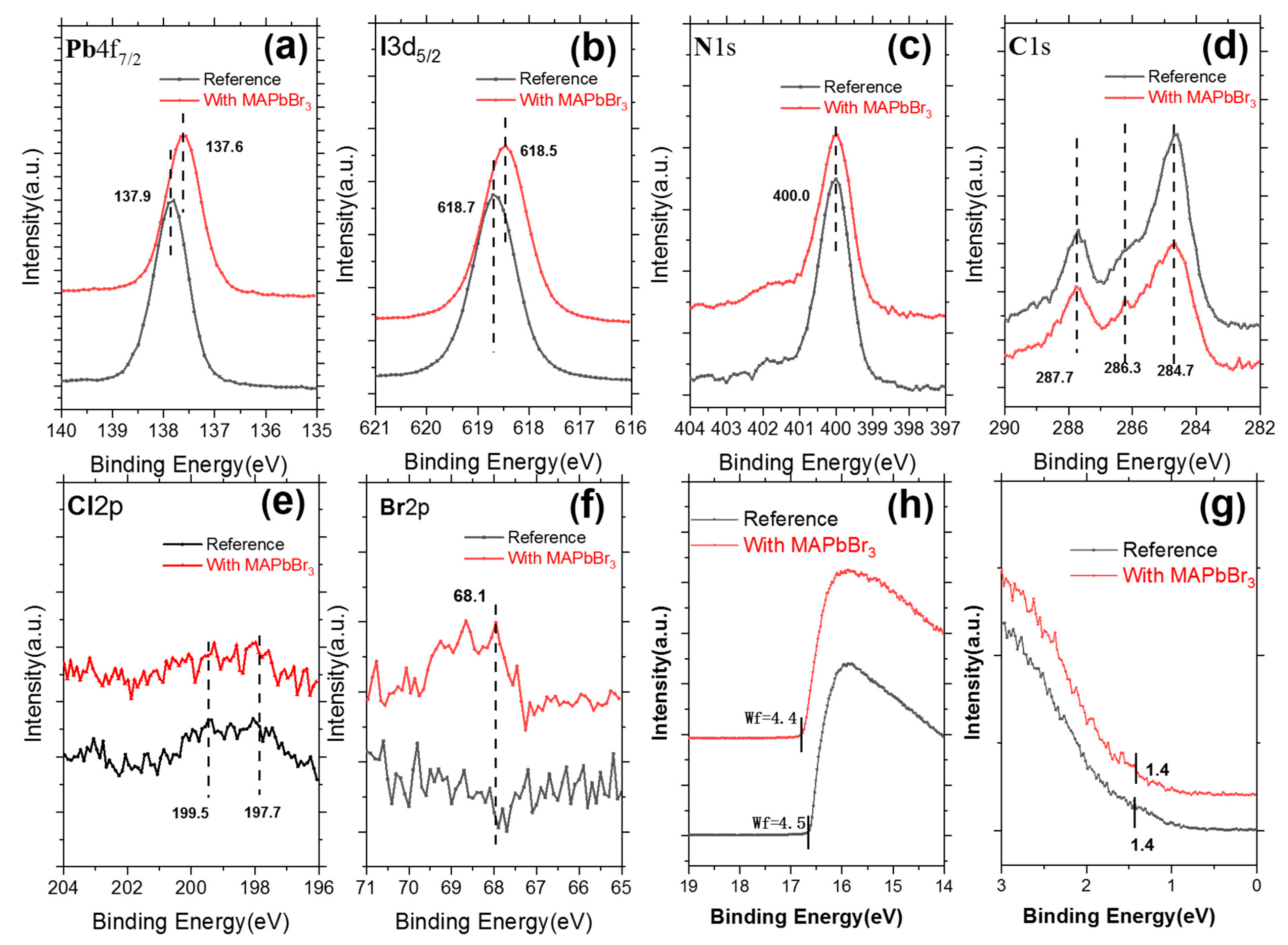
3. Results and Discussion

In situ GIWAXS measurements were carried out through the whole perovskite film fabrication process from spin-coating to annealing, as shown in Figure 1a. Figure 1b shows a schematic drawing of the in situ GIWAXS experimental setup equipped with a spin coater, heating platform, and an antisolvent syringe under nitrogen environment. The GIWAXS patterns of perovskite films with and without MAPbBr3 taken during spin-coating and annealing are present in Figure 2 and Figure 3, respectively.
Figure 2a presents the GIWAXS pattern at the beginning of spin-coating of a undoped FAPbI3 perovskite film, where no diffraction rings are visible. When chlorobenzene was dropped on the spinning films, diffraction rings instantly appeared near q = 8.3 nm−1 (Figure 2b), which originated from the rapid crystallized non-perovskite yellow phase (δ phase) out of perovskite precursor due to saturation precipitation caused by the rapid volatilization of the polar solvent after the dropping of the antisolvent. After that, the intensity of the diffraction signal increased continuously till the end of spin-coating and Figure 2c reports the same GIWAXS pattern as Figure 2b with enhanced diffraction signals. To quantify the crystallization evolution, the q-dependent 1D-XRD spectra derived from GIWAXS patterns from 4 nm−1 to 14 nm−1 are present in Figure 2g. It is clear that there is only a peak at q = 8.3 nm−1 present in the spectra after CB dropping, which indicates that only non-perovskite yellow phase (δ phase) forms during spin-coating in the film without MAPbBr3, in line with previous reports [17,18].
Figure 2d reports GIWAXS pattern of a FAPbI3 perovskite film doped by MAPbBr3 at the beginning of spin-coating, where no diffraction rings are seen. When CB was dropped (Figure 2e), a diffraction ring attributed to δ phase instantly appeared at around q = 8.3 nm−1 along with a new weak and broad diffraction ring around q = 9.9 nm−1 attributed to α phase. The intensity of these two diffraction rings gradually became stronger till the end of spin-coating and the GIWAXS pattern is reported in Figure 2f with two diffraction rings at both q = 8.4 nm−1 and q = 9.9 nm−1. The evolution of the crystallization kinetics of the MAPbBr3 doped perovskite films during spin coating can be seen well in the q-dependent 1D-XRD spectra in Figure 2h. It is obvious that the δ-phase peak shifts from 8.3 nm−1 to 8.4 nm−1 during spin-coating and is much weaker than the counterpart in Figure 2g for the film without MAPbBr3, indicating that MAPbBr3 can effectively suppress the formation of unfavorable δ phase during the spin-coating. Meanwhile, the appearance of the new α phase peak at near 9.9 nm−1 implies that MAPbBr3 can trigger the formation of black α phase perovskite even during spin-coating. All these GIWAXS results obtained during spin-coating prove that MAPbBr3 can change the crystallization pathway of FAPbI3 perovskite precursors possibly by reducing the phase transition barrier from δ phase to α phase at room temperature.
To study the crystallization kinetics during annealing, Figure 3a reports the GIWAXS pattern of the undoped FAPbI3 perovskite film without MAPbBr3 at the beginning of annealing, where the diffraction ring at near q = 8.3 nm−1 is clear but with no visible features around q = 10 nm−1, consistent with the GIWAXS image at the end of spin-coating (Figure 2c). After 3 min of annealing in Figure 3b, the diffraction ring at near q = 8.3 nm−1 becomes weaker with a new diffraction ring appearing at q = 9.9 nm−1, indicating that the non-perovskite δ phase starts to transform to the black α phase during annealing. As can be seen from the corresponding q-dependent 1D-XRD spectra in Figure 3g, the peak intensity of the δ phase is still much higher than that of the α phase at this time, implying that the δ phase is still dominant at this time. After 20 min at the end of annealing, the diffraction ring at near q = 8.3 nm−1 completely disappears whereas the diffraction ring at near q = 9.9 nm−1 becomes much stronger in Figure 3c, indicating the completion of the FAPbI3 perovskite film fabrication. Meanwhile, a very weak diffraction ring appears at near q = 9.1 nm−1, ascribed to the (001) crystal plane of PbI2 [18,19,20,21]. This confirms the existence of a small amount of excess PbI2 in the film, which indicates that PbI2 was not completely converted to perovskite [8,22,23].
In contrast to the film without MAPbBr3, two diffraction rings at both q = 8.3 nm−1 and q = 9.9 nm−1 are already present in the film doped by MAPbBr3 at the beginning of annealing (Figure 3d), consistent with the results in Figure 2f at the end of spin-coating. After 3 min of annealing (Figure 3e), the δ phase diffraction ring at near q = 8.3 nm−1 becomes much weaker whereas the α phase diffraction ring at near q = 9.9 nm−1 becomes much stronger. The corresponding q-dependent 1D-XRD spectrum at this time in Figure 3h further indicates that the α phase already becomes dominant in the film. At the end of the annealing (Figure 3f), the α phase diffraction ring becomes even brighter without any sign of δ phase diffraction feature q = 8.3 nm−1. It is also noticed that no obvious excess PbI2 formation is seen. The peak areas were calculated to determine the phase contents quantitatively. After annealing, the areas of α-phase (001) peak are 18 (a.u.) in the undoped sample and 26.6 (a.u.) in the sample of perovskite with MAPbBr3 respectively, and the undoped sample exhibited the obvious δ phase with the peak area of 0.02 (a.u.). All these GIWAXS results indicate that MAPbBr3 can facilitate the full conversion of perovskite precursors into optically active α phase perovskite during annealing.
To better understand the influences of MAPbBr3 on fabricated FAPbI3 perovskite films, photoelectron spectroscopy characterization was performed for fabricated films with and without MAPbBr3 as shown in Figure 4. For the undoped film, the Pb 4f7/2 (Figure 4a) and I 3d5/2 (Figure 4b) are located at 137.9 eV and 618.7 eV, respectively. After MAPbBr3 doping, Pb 4f7/2 and I 3d5/2 shift to lower binding energy by ~0.3 eV and ~0.2 eV, respectively. In the meanwhile, N 1s (Figure 4c) and C 1s (Figure 4f) barely change their binding energies after MAPbBr3 doping. Thus, the present XPS results suggest that MAPbBr3 could interact with FAPbI3 leading to electron transfer mainly from Pb-I octahedron, possibly due to higher electron affinity of Br anion from MAPbBr3, which may lead to its increased structural stability.
To find out the film chemical composition, Table 1 reports the atomic ratio calculated from XPS of all the elements in the fabricated films with and without MAPbBr3. It is noticed that the concentration of Cl is low with an atomic ratio of 0.02~0.01 for the two films in Table 1; however, the concentration of Cl in the precursor solution is about 0.5 mol/mL (equivalent to 35.7% of Pb ions), implying that Cl must escape from the film surface during the crystallization of perovskite in line with the previous reports [4,8]. It can be seen that the atomic ratio of Br in the film with MAPbBr3 is only 0.06 in Table 1 in contrast to 0.21 mol Br ions in 1 mL precursor solution (equivalent to 15% of Pb ions), which is also probably due to partial escaping of Br ions from the surface. As Table 1 yields an estimated atomic ratio of I:Br to be 2.85:0.06 for the film doped by MAPbBr3, its chemical structure is thus deduced as (FAPbI3)0.98(MAPbBr3)0.02.
To study the changes of electronic structure induced by MAPbBr3, the perovskite UPS spectra at the secondary electron cut-off (SECO) and valence band (VB) regions are shown in Figure 4g,h, respectively. As shown in Figure 4g, the work function (WF) of the undoped perovskite film derived from its SECO is ~4.5 eV, consistent with reported WK of FAPbI3 [24,25]. After doping with MAPbBr3, the WF is slightly deduced to 4.4 eV. As can be seen from Figure 4h, the valence band maximum (VBM) position before and after the doping of MAPbBr3 barely changes at 1.4 eV. Thus, the ionization energies (IE) of doped and undoped films are calculated to be 5.9 eV and 5.8 eV, respectively. Spiro-OMeTAD are widely used as hole transport layer (HTL) in PSCs and its IE is 5.2 eV [26,27]. Using Spiro-OMeTAD as HTL, the hole injection barriers ΔEv for the doped and undoped FAPbI3 are deduced to be 0.7 eV and 0.6 eV, respectively. As a smaller ΔEv will contribute to efficient injection of holes [21,24,25], MAPbBr3 additive in perovskite thus modifies the electronic structure of FAPbI3 with favorable interfacial energy alignment at the perovskite/spiro-OMeTAD interface.
Based on the synchrotron radiation based GIWAXS and photoemission results, we proposed a model depicting crystallization process of FAPbI3 from the perovskite precursors with or without MAPbBr3 as shown as Figure 5. It is worth mentioning that the role of Cl ions in precursor solution influencing the crystallization process is neglected in this model. The whole crystallization process can be divided into three processes in the proposed model: (1) after the anti-solvent dropping, δ phase preferentially forms in the undoped precursor solution, whereas a mixture of δ phase and α phase forms after the doping of MAPbBr3 in the precursor solution; (2) at the initial stage of annealing, the δ phase in the undoped film starts to transfer to α phase perovskite, whereas the existing α phase perovskite in the doped film becomes dominant quickly at this stage with the presence of MAPbBr3; and (3) finally, the δ phase in undoped films completely disappears and converts to α phase in both films. In the doped film, the large FA+ ions will be partially replaced by MA+ ions leading to formation of (FAPbI3)0.98(MAPbBr3)0.02.
To check the morphology changes induced by MAPbBr3 doping, scanning electron microscopy (SEM) and atomic force spectroscopy (AFM) measurements were carried out with data shown in Figure 6. As can be seen from the SEM image in Figure 6a, the undoped film presents large grains with an average size over a few microns as well as some pinholes near the grain boundaries, which normally is associated with the rapid nucleation process [28]. After the addition of MAPbBr3 (Figure 6b), the doped film looks denser and more compact with smaller grain and almost no pinholes near the grain boundaries. As it is reported that MACl can promote the growth of perovskite crystal grains making the large grains [4,29,30], the Br anion from MAPbBr3 could slowly diffuse during the perovskite film formation process, which slows down the rapid growth of perovskite grains, with defect density significantly reduced [4]. The improved morphology is also evidenced by AFM images in Figure 6c,d: the grains in the undoped film are more irregular whereas the grains in the doped film are more uniform and dense with fewer defects, in consistency with SEM results.
In order to study the effect of MAPbBr3 on the optical properties of the perovskite layers, we conducted UV-visible absorption spectroscopy and photoluminescence spectrum (PL) of doped and undoped films. The absorption wavelength of the perovskite film doped with MAPbBr3 is blue-shifted from 805.2 nm to 790.1 nm, as shown in Figure 7b, which corresponds to a band gap shift from 1.54 eV to 1.57 eV. The PL results (Figure 7c) followed a similar tendency to the UV-visible absorption: the emission peak showed a blue-shift from 825.0 nm to 814.2 nm with increased peak intensity, suggesting a lower carrier recombination due to the improved crystal quality.
To investigate the impact of MAPbBr3 on FAPbI3 based photovoltaic device performances, PSCs using FAPbI3 perovskite with and without MAPbBr3 additive were fabricated and the device structure was ITO/SnO2/perovskite/Spiro-OMeTAD/MoO3/Ag, as shown in Figure 7d. The current density-voltage (J-V) curve of these PSCs and their corresponding J-V parameters are shown in Figure 7e. The champion power conversion efficiency (PCE) of the control devices based on undoped FAPbI3 is only 14.2%, with a short current density (Jsc) of 23.7 mA cm−2, an open circuit voltage (Voc) of 0.99 V and a filling factor (FF) of 60.4%. The MAPbBr3 doped FAPbI3 based PSCs yielded a champion PCE up to 19.4%, which was mainly attributed to the significant enhancement of Voc of 1.11 V and FF of 72%. The devices with MAPbBr3 exhibit negligible hysteresis, and the J-V curves of perovskite with MAPbBr3 devices prepared for both forward and reverse scans are shown in Figure 7f. The enhanced performance of PSCs should be attributed to the improved film quality with reduced defects density as well as the optimization of band alignment at the perovskite/sprio-OMeTAD interface by introducing MAPbBr3 additive into the FAPbI3 precursors.

4. Conclusions

In summary, we investigated the crystallization kinetic process of FAPbI3 perovskite precursor solutions with and without MAPbBr3 additive by using in situ synchrotron radiation based GIWAXS during both spin-coating and annealing. It was found that MAPbBr3 can effectively suppress δ-phase formation while promoting α-phase formation during spin-coating, resulting in a high-quality film without PbI2 residue. Combined with the photoelectron spectroscopy analysis, a model about the FAPbI3 crystallization kinetics was proposed. Furthermore, PL results also demonstrate the improved crystalline quality. Finally, performances of devices were analyzed together with other characterizations. Finally, PSCs based on MAPbBr3-doped FAPbI3 were fabricated with a champion efficiency as high as 19.4% from 14.2% for the PSCs based on undoped FAPbI3.

Author Contributions

Conceptualization, Z.S. and X.G.; Data curation, Z.S. and C.W.; Formal analysis, Z.S., C.W. and G.Z.; Funding acquisition, X.G.; Investigation, Z.S., C.W. and G.Z.; Methodology, Z.S. and C.W.; Project administration, G.Z. and X.G.; Resources, X.G.; Supervision, X.G. All authors have read and agreed to the published version of the manuscript.

Funding

This work is supported by the National Key Research and Development Program of China (Grant Nos. 2017YFB0701901, 2017YFA0403400, 2017YFA0402900) and the Natural Science Foundation of China (Grant Nos. 11675252, U1632265, and 12074385).

Institutional Review Board Statement

Not applicable.

Informed Consent Statement

Not applicable.

Data Availability Statement

Data sharing is not applicable to this article.

Conflicts of Interest

The authors declare no conflict of interest.

References

  1. Green, M.A.; Dunlop, E.D.; Hohl-Ebinger, J.; Yoshita, M.; Kopidakis, N.; Ho-Baillie, A.W. Solar cell efficiency tables (Version 55). Prog. Photovolt. 2020, 28, 3–15. [Google Scholar] [CrossRef]
  2. Ke, W.; Fang, G.; Liu, Q.; Xiong, L.; Qin, P.; Tao, H.; Wang, J.; Lei, H.; Li, B.; Wan, J. Low-temperature solution-processed tin oxide as an alternative electron transporting layer for efficient perovskite solar cells. J. Am. Chem. Soc. 2015, 137, 6730–6733. [Google Scholar] [CrossRef]
  3. Jiang, Q.; Zhang, L.; Wang, H.; Yang, X.; Meng, J.; Liu, H.; Yin, Z.; Wu, J.; Zhang, X.; You, J. Enhanced electron extraction using SnO2 for high-efficiency planar-structure HC (NH2)2PbI3-based perovskite solar cells. Nat. Energy 2016, 2, 1–7. [Google Scholar] [CrossRef]
  4. Yoo, J.J.; Seo, G.; Chua, M.R.; Park, T.G.; Lu, Y.; Rotermund, F.; Kim, Y.-K.; Moon, C.S.; Jeon, N.J.; Correa-Baena, J.-P. Efficient perovskite solar cells via improved carrier management. Nature 2021, 590, 587–593. [Google Scholar] [CrossRef]
  5. Turren-Cruz, S.-H.; Hagfeldt, A.; Saliba, M. Methylammonium-free, high-performance, and stable perovskite solar cells on a planar architecture. Science 2018, 362, 449–453. [Google Scholar] [CrossRef] [PubMed] [Green Version]
  6. Saliba, M.; Matsui, T.; Seo, J.-Y.; Domanski, K.; Correa-Baena, J.-P.; Nazeeruddin, M.K.; Zakeeruddin, S.M.; Tress, W.; Abate, A.; Hagfeldt, A. Cesium-containing triple cation perovskite solar cells: Improved stability, reproducibility and high efficiency. Energy Environ. Sci. 2016, 9, 1989–1997. [Google Scholar] [CrossRef] [PubMed] [Green Version]
  7. Li, Q.; Zhao, Y.; Fu, R.; Zhou, W.; Zhao, Y.; Liu, X.; Yu, D.; Zhao, Q. Efficient Perovskite Solar Cells Fabricated Through CsCl-Enhanced PbI2 Precursor via Sequential Deposition. Adv. Mater. 2018, 30, 1803095. [Google Scholar] [CrossRef]
  8. Ye, F.; Ma, J.; Chen, C.; Wang, H.; Xu, Y.; Zhang, S.; Wang, T.; Tao, C.; Fang, G. Roles of MACl in Sequentially Deposited Bromine-Free Perovskite Absorbers for Efficient Solar Cells. Adv. Mater. 2021, 33, 2007126. [Google Scholar] [CrossRef]
  9. Kojima, A.; Teshima, K.; Shirai, Y.; Miyasaka, T. Organometal halide perovskites as visible-light sensitizers for photovoltaic cells. J. Am. Chem. Soc. 2009, 131, 6050–6051. [Google Scholar] [CrossRef] [PubMed]
  10. Wang, L.; Zhou, H.; Hu, J.; Huang, B.; Sun, M.; Dong, B.; Zheng, G.; Huang, Y.; Chen, Y.; Li, L. A Eu3+-Eu2+ ion redox shuttle imparts operational durability to Pb-I perovskite solar cells. Science 2019, 363, 265–270. [Google Scholar] [CrossRef]
  11. Luo, D.; Yang, W.; Wang, Z.; Sadhanala, A.; Hu, Q.; Su, R.; Shivanna, R.; Trindade, G.F.; Watts, J.F.; Xu, Z. Enhanced photovoltage for inverted planar heterojunction perovskite solar cells. Science 2018, 360, 1442–1446. [Google Scholar] [CrossRef] [Green Version]
  12. Hou, Y.; Du, X.; Scheiner, S.; McMeekin, D.P.; Wang, Z.; Li, N.; Killian, M.S.; Chen, H.; Richter, M.; Levchuk, I. A generic interface to reduce the efficiency-stability-cost gap of perovskite solar cells. Science 2017, 358, 1192–1197. [Google Scholar] [CrossRef] [Green Version]
  13. Zheng, X.; Chen, B.; Dai, J.; Fang, Y.; Bai, Y.; Lin, Y.; Wei, H.; Zeng, X.C.; Huang, J. Defect passivation in hybrid perovskite solar cells using quaternary ammonium halide anions and cations. Nat. Energy 2017, 2, 1–9. [Google Scholar] [CrossRef]
  14. Kim, M.; Kim, G.-H.; Lee, T.K.; Choi, I.W.; Choi, H.W.; Jo, Y.; Yoon, Y.J.; Kim, J.W.; Lee, J.; Huh, D. Methylammonium chloride induces intermediate phase stabilization for efficient perovskite solar cells. Joule 2019, 3, 2179–2192. [Google Scholar] [CrossRef]
  15. Jeon, N.J.; Noh, J.H.; Yang, W.S.; Kim, Y.C.; Ryu, S.; Seo, J.; Seok, S.I. Compositional engineering of perovskite materials for high-performance solar cells. Nature 2015, 517, 476–480. [Google Scholar] [CrossRef]
  16. Yang, G.; Zhang, H.; Li, G.; Fang, G. Stabilizer-assisted growth of formamdinium-based perovskites for highly efficient and stable planar solar cells with over 22% efficiency. Nano Energy 2019, 63, 103835. [Google Scholar] [CrossRef]
  17. Ma, F.; Li, J.; Li, W.; Lin, N.; Wang, L.; Qiao, J. Stable α/δ phase junction of formamidinium lead iodide perovskites for enhanced near-infrared emission. Chem. Sci. 2017, 8, 800–805. [Google Scholar] [CrossRef] [PubMed] [Green Version]
  18. Yuan, S.; Qian, F.; Yang, S.; Cai, Y.; Wang, Q.; Sun, J.; Liu, Z.; Liu, S. NbF5: A Novel α-Phase Stabilizer for FA-Based Perovskite Solar Cells with High Efficiency. Adv. Funct. Mater. 2019, 29, 1807850. [Google Scholar] [CrossRef]
  19. Shi, B.; Yao, X.; Hou, F.; Guo, S.; Li, Y.; Wei, C.; Ding, Y.; Li, Y.; Zhao, Y.; Zhang, X. Unraveling the passivation process of PbI2 to enhance the efficiency of planar perovskite solar cells. J. Phys. Chem. C 2018, 122, 21269–21276. [Google Scholar] [CrossRef]
  20. Wang, H.; Wang, Z.; Yang, Z.; Xu, Y.; Ding, Y.; Tan, L.; Yi, C.; Zhang, Z.; Meng, K.; Chen, G. Ligand-Modulated Excess PbI2 Nanosheets for Highly Efficient and Stable Perovskite Solar Cells. Adv. Mater. 2020, 32, 2000865. [Google Scholar] [CrossRef] [PubMed]
  21. Ji, G.; Zhao, B.; Song, F.; Zheng, G.; Zhang, X.; Shen, K.; Yang, Y.; Chen, S.; Gao, X. The energy level alignment at the CH3NH3PbI3/pentacene interface. Appl. Surf. Sci. 2017, 393, 417–421. [Google Scholar] [CrossRef]
  22. Jacobsson, T.J.; Correa-Baena, J.-P.; Halvani Anaraki, E.; Philippe, B.; Stranks, S.D.; Bouduban, M.E.; Tress, W.; Schenk, K.; Teuscher, J.L.; Moser, J.-E. Unreacted PbI2 as a double-edged sword for enhancing the performance of perovskite solar cells. J. Am. Chem. Soc. 2016, 138, 10331–10343. [Google Scholar] [CrossRef] [Green Version]
  23. Tumen-Ulzii, G.; Qin, C.; Klotz, D.; Leyden, M.R.; Wang, P.; Auffray, M.; Fujihara, T.; Matsushima, T.; Lee, J.W.; Lee, S.J. Detrimental Effect of Unreacted PbI2 on the Long-Term Stability of Perovskite Solar Cells. Adv. Mater. 2020, 32, 1905035. [Google Scholar] [CrossRef] [PubMed]
  24. Ji, G.; Zheng, G.; Zhao, B.; Song, F.; Zhang, X.; Shen, K.; Yang, Y.; Xiong, Y.; Gao, X.; Cao, L. Interfacial electronic structures revealed at the rubrene/CH3 NH3 PbI3 interface. Phys. Chem. Chem. Phys. 2017, 19, 6546–6553. [Google Scholar] [CrossRef]
  25. Zhang, X.; Su, Z.; Zhao, B.; Yang, Y.; Xiong, Y.; Gao, X.; Qi, D.-C.; Cao, L. Chemical interaction dictated energy level alignment at the N, N′-dipentyl-3, 4, 9, 10-perylenedicarboximide/CH3NH3PbI3 interface. Appl. Phys. Lett. 2018, 113, 113901. [Google Scholar] [CrossRef] [Green Version]
  26. Jiménez-López, J.; Cambarau, W.; Cabau, L.; Palomares, E. Charge injection, carriers recombination and HOMO energy level relationship in perovskite solar cells. Sci. Rep. 2017, 7, 1–10. [Google Scholar]
  27. Jeon, N.J.; Lee, H.G.; Kim, Y.C.; Seo, J.; Noh, J.H.; Lee, J.; Seok, S.I. o-Methoxy substituents in spiro-OMeTAD for efficient inorganic–organic hybrid perovskite solar cells. J. Am. Chem. Soc. 2014, 136, 7837–7840. [Google Scholar] [CrossRef] [PubMed]
  28. Meng, X.; Lin, J.; Liu, X.; He, X.; Wang, Y.; Noda, T.; Wu, T.; Yang, X.; Han, L. Highly Stable and Efficient FASnI3-Based Perovskite Solar Cells by Introducing Hydrogen Bonding. Adv. Mater. 2019, 31, 1903721. [Google Scholar] [CrossRef]
  29. Lin, K.; Xing, J.; Quan, L.N.; de Arquer, F.P.G.; Gong, X.; Lu, J.; Xie, L.; Zhao, W.; Zhang, D.; Yan, C. Perovskite light-emitting diodes with external quantum efficiency exceeding 20 percent. Nature 2018, 562, 245–248. [Google Scholar] [CrossRef]
  30. Zhang, H.; Lv, Y.; Wang, J.; Ma, H.; Sun, Z.; Huang, W. Influence of Cl incorporation in perovskite precursor on the crystal growth and storage stability of perovskite solar cells. ACS Appl. Mater. Interfaces 2019, 11, 6022–6030. [Google Scholar] [CrossRef] [PubMed]
Figure 1. Schematics of the film fabrication procedure and the experimental setup for in situ GIWAXS measurement. (a) The steps of perovskite fabrication process and (b) The in situ GIWAXS experimental setup equipped with a spin coater, heating platform, and an antisolvent syringe under nitrogen environment.
Coatings 11 00545 g001
Figure 2. The 2D GIWAXS patterns taken at different times during spin-coating for an undoped film in (ac) and for a MAPbBr3-doped perovskite film in (df), respectively. The derived 1D XRD spectra for the undoped film in (g) and for the MAPbBr3-doped perovskite film in (h), respectively.
Coatings 11 00545 g002
Figure 3. The 2D GIWAXS patterns taken at different time points during annealing for the undoped film in (ac) and for the MAPbBr3-doped perovskite film in (df), respectively. The derived 1D XRD spectra for the undoped film in (g) and for the MAPbBr3-doped perovskite film in (h), respectively.
Coatings 11 00545 g003
Figure 4. (a) Pb 4f7/2, (b) I 3d5/2, (c) N 1s, (d) C 1s, (e) Cl 2p, (f) Br 2p core-level spectra, and (h) SECO and (g) VB spectra for perovskite films with and without MAPbBr3.
Coatings 11 00545 g004
Figure 5. The schematic diagram depicting the crystallization process of FAPbI3 perovskite films with and without MAPbBr3 additive.
Coatings 11 00545 g005
Figure 6. Top-view scanning electron microscopy (SEM) images (upper panel) and atomic force spectroscopy (AFM) images (lower panel) of perovskite films with or without MAPbBr3 additive: (a,c) the undoped perovskite film and (b,d) the MAPbBr3-doped perovskite film.
Coatings 11 00545 g006
Figure 7. (a) The energy level diagram for the SnO2/perovskite/sprio-OMeTAD PSCs; (b) the absorption spectrum of perovskite on quartz; (c) the PL spectrum of perovskite on quartz; (d) the device architecture; (e) J-V curves of PSCs based on films with and without MAPbBr3 additive; (f) J-V curves of perovskite with MAPbBr3 devices prepared for both forward and reverse scans.
Coatings 11 00545 g007
Table 1. Proportions of elements on the film surface of the reference and target samples, where the proportions of each element are relative to the content of Pb atoms.
Element ContentPbIBrCNCl
Reference1.002.9701.882.510.02
With MAPbBr31.002.850.061.722.300.01
Publisher’s Note: MDPI stays neutral with regard to jurisdictional claims in published maps and institutional affiliations.

