Abstract
ZnOTe compounds were grown by DC magnetron cosputtering from pure Tellurium (Te) and Zinc (Zn) cathodes in O2/Ar atmosphere. The applied power on the Zn target was constant equal to 100 W, while the one applied on the Te target took two values, i.e., 5 W and 10 W. Thus, two sample series were obtained in which the variable parameter was the distance from the Te targets to the substrate. Sample compositions were determined by Rutherford Backscattering Spectroscopy (RBS) experiments. Structural analysis was done using X-Ray diffraction (XRD) spectrometry and the growth of the hexagonal w-ZnO phase was identified in the XRD spectra. RBS results showed high bulk homogeneity of the samples forming ZnOTe alloys, with variable Te molar fraction (MF) ranging from 0.48–0.6% and from 1.9–3.1% for the sample series obtained at 5 W and 10 W, respectively. The results reflect great differences between the two sample series, particularly from the structural and optical point of view. These experiments point to the possibility of Te doping ZnO with the permanence of intrinsic defects, as well as the possibility of the formation of other Te solid phases when its content increases. The results and appreciable variations in the band gap transitions were detected from Photoluminescence (PL) measurements.
1. Introduction
Zinc Oxide (ZnO) is a well-known II–VI semiconductor with direct band gap around 3.37 eV and large exciton binding energy (60 meV) at room temperature [1]. Nowadays, ZnO and ZnO-based materials are recognized in a wide spectrum of applications, which make them into unique materials because of the combination of multiple functional properties including electronics and human healthcare. However, the large range of industrial uses is strongly dependent on the experimental technique, parameters, preparation, and post-treatment of the grown samples etc. Optimizing these factors is the greatest challenge in obtaining these materials’ benefits.
Multiple research projects and the discovery of new applications for materials based on ZnO made this semiconductor the focus of important high-technology advances, such as optoelectronic devices, particularly those based on ZnO nanostructured for light emitters [2,3]. ZnO thin film transistors under ultraviolet irradiation [4], broad band photo-absorption architectures from UV-IR [5], gas sensors [6], acoustic wave devices, solar cells, transparent electronic and flat panel displays [7,8,9], and photo-catalytic applications [10] etc. The ZnO wideband gap and transparency in thin film form makes it a prominent candidate for use in multiband materials, especially for enhancing solar cell efficiency [11]. Great challenges in the last decade include synthesizing ZnO-based materials that allow for control over p-type doping [12,13] and building n- and p- type based semiconductor junctions [14]. Currently, ternary compounds combining Zn, O, and Te atoms acquired great significance for developing Highly Mismatched Alloys (HMA) mainly with the goal of enhancing solar cell efficiency. The band structure obtained this way is well-described by the band anticrossing (BAC) model [15], which showed that dilute impurities lead to an unusual energy band structure with a narrow band of states located in the band gap of the host material [16,17]. In particular, Te may provide advantages if it is used as an isoelectronic dopant [18,19]. Up to now, both undoped ZnO and ZnO:Te alloys as well as ZnTe:O were grown using several deposition techniques, such as: ion implantation followed by pulsed laser melting (PLM) [20], chemical precipitation [10], molecular beam epitaxy (MBE) [12], atomic layer deposition [21], hydrothermal method [22,23] etc. Recently, Ting et. al. [24] published an interesting paper dealing with different parameters affecting the growth of ZnTeO alloys and their influence in band gap modulation. In the field of Sputtering deposition techniques, RF magnetron sputtering is the most common [25,26], particularly with ZnTe as the unique target, to obtain ZnTeO alloys [27]. Recently, RF magnetron sputtering using two independent targets of ZnTe and ZnO was also used [28]. All these techniques were used indistinctly for both ZnO-based thin films and nanostructured compounds. Nevertheless, there are few reports on DC magnetron sputtering for growing such materials and even less for those using the DC cosputtering magnetron. The main objective of this basic research was to study the effects of low and middle Te concentrations in the ZnO network which currently constitute an interesting scientific issue. For this purpose, ZnO:Te thin films with different Tellurium atomic content and without any intentional heating were grown by using two separate, highly pure, and independent targets of Te and Zn. Under these experimental conditions, we were able to get high control of the ZnOTe thin film composition. Sputtering deposition is widely used for thin films growth because of its ability to cover large surface areas, which makes it easy to scale to an industrial level at a relatively low cost. We carried out compositional, structural, and optoelectronic characterization to study the influence of Te content on the macroscopic properties of the samples. As far as we know, this is the first report of the growth and procedures to obtain ZnOTe alloys by DC magnetron cosputtering technique with independent Zn and Te cathodes.
2. Materials and Methods
ZnO:Te films were deposited onto monocrystalline (<100>) n-type silicon substrates by using a DC magnetron cosputtering system. The reaction chamber consists of a vacuum cylindrical enclosure where two circular, 7.62 cm in diameter planar magnetrons are located. The distance between them was set at 60° so that the samples were exposed to both cathodes during the growth processes. Then the substrates were cleaned in successive ultrasonic baths (acetylene trichloro, acetone, ethanol, and deionized water) to degrease and to eliminate rests of strange materials on their surfaces. Finally, they were dried under nitrogen flow. Highly pure commercial Zinc (99.99%) and Tellurium (99.99%) were used as targets (cathodes). All experiments were performed in an Ar (99.999%) and O2 (99.992%) atmosphere keeping the O2/Ar ratio equal to 0.24%, and deposition time was maintained at 30 min. The chamber was pumped out to a base pressure of −4 Pa with the working pressure equal to −1 Pa. The Zn-cathode distance to the substrate (DZn–S) and the applied power on the Zn target (PZn) remained constants, equal to 15 cm and 100 W respectively. These experimental parameters are the optimal parameters for obtaining highly stoichiometric and crystalline ZnO thin films, as we previously reported [29].
Prior to deposition, the targets were presputtered for 10 min to remove any impurity on their surfaces. The samples were grown after the total poisoning of the cathodes working under the reactive sputtering regime. We reported that higher Te content leads to faster ZnO structure amorphization [29]. To deepen the study on the effects of the incorporation of Te in ZnO structure and the experimental conditions, two sample series (A and B) were obtained in the present study; the experimental conditions are displayed in Table 1. The film thicknesses were measured using a mechanical stylus profilometer (Veeco Dektak 150, Plainview NY, USA).

Table 1.
Sample labels, experimental parameters, and thicknesses. DTe-S: Te: cathode-sample relative distance; PTe: power applied on Te and Zn target, DZn-S: Zn cathode-substrate relative distance; hp: sample thicknesses.
Sample compositions were determined by Rutherford Backscattering Spectroscopy (RBS) in the 5 MV HVEE Tandetron accelerator at the Micro-Analysis Centre of Materials (CMAM) at the Universidad Autónoma de Madrid (UAM). To register RBS spectra, a He beam (3070 keV) with scattering angle of 170.5° was used. At this energy, the scattering cross section with oxygen shows a resonance increasing the Rutherford value by a factor of almost 25 [30]. RBS spectra were simulated using SIMNRA software [31]. The samples’ thicknesses were also measured with this technique to compare them with that of those measured by profilometry. X-Ray Diffraction (XRD) spectra were registered with a Siemens D-5000 Diffractometer (Berlin, Germany) using grazing incidence geometry (Cu anode; Kα = 0.1542 nm) with a fixed incidence angle of 0.5° at room temperature to determine the crystalline structure of the films. Transmission spectrophotometry spectra were registered by using a SolidSpec-3700 Spectrophotometer (Shimadzu, Kyoto, Japan) in the range of 190–800 nm. Photoluminescence (PL) measurements in the UV—Visible range were also carried out by means of a Labram system model HR800 UV (Horiba, Kyoto, Japan) provided with a He-Cd laser (325 nm).
3. Results and Discussion
3.1. Film Composition and RBS Analysis
Fitting of the RBS spectra was done by means of thin layers composed of nonstoichiometric compounds of Zn, Te, and O atoms along their thicknesses. Simulated RBS spectra (as illustrated in Figure 1) were adjusted, editing each sample composition with a small number of layers indicative of high homogeneity in the distribution of the elements in depth. The resulting empirical formulas shown in Table 2 reflect the high chemical composition control reached by DC magnetron cosputtering technique and the experimental procedures used in this work. From the empirical formulas, it is notable that in the case of the A sample series, the Te atomic percent ranges from 0.48–0.6%, while in the B sample series, this parameter ranges from 1.9–3.1% over the entire atomic composition of the samples. It is expected that this marked difference of an order of magnitude in Tellurium content between both series leads to significant changes in their macroscopic properties. It can be considered a strong agreement between the thickness values obtained by profilometry and RBS measurements (see hP/h1 ratio in Table 2). Regarding the excess oxygen detected in all samples, it is linked to the growing atmosphere. This excess with respect to the Zinc element is shown in the right column in Table 2. Also of note are the different Te incorporations in both series depending on the relative distances between Te cathode and the substrate DTe-S, particularly drawing attention to the case of sample series B. The different behavior of the ratios Te/Zn and Te/O are represented in Figure 2.
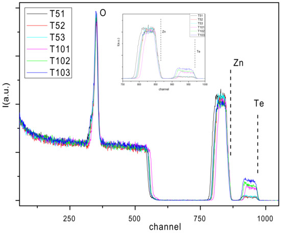
Figure 1.
Rutherford Backscattering Spectroscopy (RBS)-fitted spectra from all samples. Zoom inset shows the different Zn and Te concentration profiles more clearly.
Table 2.
RBS thicknesses; hp/h1: Profilometry/RBS thicknesses ratio; [Te]: Te Molar Fraction × 1015 Atoms/cm2; ECF: Empirical Chemical Formula and O/Zn: Oxygen/Zinc atomic composition ratio.
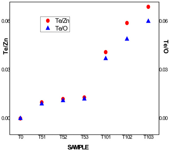
Figure 2.
Te/Zn and Te/O ratios behavior for both sample series.
While in series A, both ratios increased very slowly, tending to a saturation value around 0.013, in series B, both atomic ratios increased almost monotonically and inversely proportional to the distance between the Te cathode and the substrate. Evidently, in our experimental conditions for the lowest PTe applied on the Tellurium cathode, the parameter DTe-S did not have a significant role in the Te incorporation into the films, in contrast with sample series B which obtained with the highest PTe value. In this case, the following microscopic events could have happened:
- (a)
- Partial substitution of Zn by Te atoms in the ZnO crystalline structure is possible since it is higher in sample series B.
- (b)
- Considering the increasing Te content and oxygen excess, it is possible the Zn vacancies or interstitials were quenched by oxygen ionic species or oxygen substitution by Te atoms in different chemical ionization states.
- (c)
- Formation of other nonstoichiometric and probably amorphous Te-O compounds. Neither were discarded.
All the above phenomena could take place in one sample at the same time depending on multiple experimental parameters, on the chemical ionization states, and the concentrations of impurities. Additional in-depth studies to elucidate those extremes are needed.
3.2. Crystalline Structure
XRD spectra of the A and B sample series are shown in Figure 3a,b, respectively. In both figures, the spectra were displaced vertically for clarity. The reference spectrum from ZnO appears at the top of Figure 3 to facilitate comparison. The intensities and Full Width at Half Maximum (FWHM) from the main crystallographic orientations point to a low crystalline quality in this reference. Vertical black dot lines were drawn as a visible guide for identifying positions of the main Bragg reflections detected after Gaussian adjustment of the peaks identified in the ZnO diffractogram. The main crystallographic orientations denoting the formation of polycrystalline hexagonal phase [32] w-ZnO is more strongly manifested in the spectra of samples with the lowest Te content in both series. In sample series A (as illustrated in Figure 3a), for sample T51, the Bragg reflections observed in the w-ZnO reference are clearly identified. However, the peak associated with the <101> crystallographic orientation of w-ZnO becomes the most intense, instead of the one corresponding to <002> crystallographic orientation as is generally accepted for this ZnO phase. On the other hand, it is possible to identify a very weak Bragg reflection in this sample, around 2θ = 43.21°, which was attributed to the <220> crystallographic orientation of ZnTe cubic phase (b-ZnTe) [33,34]. In this series, for higher Te content, i.e., samples T52 and T53, the <002> crystallographic orientation becomes prominent. It is significant that in the T53 sample diffractogram with the highest Te content, the w-ZnO structure was noticeably weakened, with the presence of a unique broad peak along the <002> orientation. These observations can lead to the suspicion that important structural changes occurred in the samples with increasing Te content which will be more evident in the following analysis. Particularly, in the aforementioned fits, slight shifts were observed in the positions of the most pronounced diffraction peaks characterizing w-ZnO with the incorporation of Te atoms in its framework.
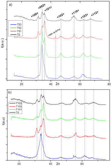
Figure 3.
X-Ray Diffraction (XRD) spectra of (a) sample series A and (b) sample series B. The XRD spectrum of ZnO appears at the top as reference. Vertical black dot lines aim to facilitate the identification of the main crystallographic orientations of reference. The spectra were displaced vertically for clarity.
This fact is displayed in Table 3. We found that the FWHM of the diffraction peaks increases considerably for all samples relative to their counterparts in the reference sample. Especially in sample T103, this parameter could achieve more than nine units of difference with respect to that estimated for the same Bragg reflection in the sample reference. The latest agree with the loss of w-ZnO crystalline quality when Te content increases as mentioned above.
Table 3.
2θ position variations of main crystallographic orientation from w-ZnO as Te content increases for all samples. NI stands for Not Identifiable.
The shift to smaller angles indicates an increase in the interplanar distances, which implies the possibility of Tellurium incorporation into the ZnO network, substituting either Zn or O atoms [10]. The diffractograms of sample series B are shown in Figure 3b. A weak although recognizable w-ZnO phase is present in all spectra. In this case, the <101> crystallographic orientation is predominant in samples T101 and T102, as it was in sample T51 from series A. However, here, sample T103 with the highest Te content in absolute terms shows only a very wide band centered at 2θ = 33.9, which could be also associated with the w-ZnO <002> crystallographic orientation as the best approximation. This band is broader than that observed in sample T53 at 2θ = 34.2 degrees. In this sample series, it is also possible to detect a slight drift to smaller 2θ angles of the peaks at the <002> and <101> crystallographic orientations (as illustrated in Table 3).
To go deeper into the structural changes of the grown samples, additional calculations of the received XRD spectra are displayed in Table 4. The following equations were used:
where β = FWHM of the peak at 2θ locations also identified and λ is the wavelength of the X-Ray radiation.
Φ: mean crystallite size = 0.9λ/βcos(θ) with λ = 0.1542 nm
Ɛ: Microstrain = β/4tan(θ)
δ: Dislocation density = 1/Φ2
According to Debey–Scherrer equations [35,36], the Unitary Cell Volume (UCV) is given by
UCV = (3/2)(5)1/2 (a2c)
Table 4.
Crystallite sizes, strains, and dislocation densities calculated for <002> crystalline orientation and UCV of the samples.
Table 4.
Crystallite sizes, strains, and dislocation densities calculated for <002> crystalline orientation and UCV of the samples.
| SAMPLE | 2θ | β (Degrees) | Φ (nm) | Ɛ (×10−4) | δ (nm−2) (10−4) | UCV (nm3) |
|---|---|---|---|---|---|---|
| T0 | 34.5 | 0.4 | 20.4 | 5.6 | 23.9 | 0.1929 |
| T51 | 34.02 | 1.5 | 5.44 | 20.7 | 337.6 | 0.1909 |
| T52 | 33.98 | 1.24 | 6.58 | 17.1 | 230.7 | 0.1952 |
| T53 | 34.2 | 1.92 | 4.25 | 26.6 | 552.5 | 0.1906 |
| T101 | 33.8 | 1.66 | 4.92 | 22.7 | 413.9 | 0.1955 |
| T102 | 33.8 | 2 | 4.08 | 27.4 | 600.8 | 0.1935 |
| T103 | 33.9 | 2.64 | 3.09 | 36.2 | 1046.3 | 0.1956 |
XRD analysis allows us to determine abrupt changes in the crystalline structures of the samples deposited at different powers as well as the different distances between the Te cathode and the substrate. Increasing the content of Te results in an irregular loss of crystalline quality of w-ZnO in both sample series with respect to the reference. Higher Te content corresponds to greater effects on the crystalline structure of ZnO. The great diminution of the particle size when Te content increases is presented in Table 4.
The most significant feature is the progressive increase in the dislocation density, which is associated with the presence of defects, impurities, atomic mismatches, and the stress with the nearest atoms produced by the possible Te incorporation into the w-ZnO network, etc. It was previously reported that the increase in dislocation density acts as an indicator for the increase in sample defects [37].
Considering the relationships between the ion radii, valences, and electronegativity of the three elements, it is possible that both the substitution of Zn and O by Te atoms could occur in the ZnO network for low Te content. Nonetheless, substitution of Zn atoms by Te atoms should be easier according to solid solutions theory [38]. Evidently, the FWHM of the Bragg reflection <002> increases from 0.4° for the reference sample (T0) up to 2.64° for the sample T103 (as illustrated in Table 4) with the highest content of Te. This fact is also indicative of the loss of crystalline quality of the matrix. This is further corroborated by the decrease of the mean crystallite sizes and the increase of the strain, although this is less significant than the behavior of the dislocation density. In addition, the mean value calculated for the UCV was around 0.19355 nm3; this parameter behaves differently in each series too. On the one hand, we were unable to identify a clear tendency in the A series. For example, while in sample T52 it is higher than that of ZnO, samples T51 and T53 show UCV values lower than those of the ZnO reference. On the other hand, the UCV behavior observed in B series shows an increase for all samples with respect to the ZnO reference reaching a maximum deviation of 0.0027 nm3 for sample T103, which was grown at PTe = 10 W with Te cathode located in the nearest position with respect to the substrate. In general, the values achieved by the UCV are close and, in some cases, coincide with those reported by other authors [10] in the range of the lowest concentrations of Te (series A), indicating the reduction of the lattice parameters particularly in samples T51 and T53. We think that in the series A there is a partial replacement of Zn by oxygen atoms in the ZnO network, while in series B, a replacement of Zn by Te atoms in the network occurs.
From XRD results, we conclude that it is possible to obtain Te doping ZnO for the Te concentrations used in this work or lower by using the DC cosputtering magnetron technique while maintaining control of the sample compositions. As previously reported [26,27], these results could have relevant consequences for the band structure of the obtained compounds.
3.3. Optical and Photoluminescence Properties
The interpretation of photoluminescent (PL) properties of ZnO and ZnO-based materials either in thin films form or in lower dimensionality is one of the most controversial topics in the field of semiconductors and materials in general. To date, there is no complete agreement about the origins of PL emissions from these materials in their different compositions, dimensions, and configurations. This is partially due to the large number of factors that influence these properties, among them: the starting sources and concentration of species participating in the growth processes, the growth techniques and procedures used, atmospheres, relative pressures, temperatures, etc. Detailed analysis of the PL response of ZnO reference is shown in Figure 4. Two very wide and intense bands are located in the UV and Visible ranges. The particularly asymmetric defect band (DB) is centered at about 2.25 eV.
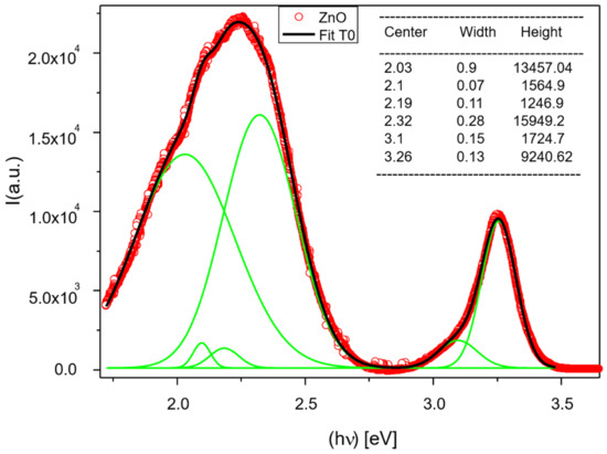
Figure 4.
UV-visible photoluminescent (PL) spectrum of sample T0. It shows experimental points, integral Gaussian fitting curve, and single curves (green) that compose this acceptable fitting.
In this figure, the existence of a large quantity of intrinsic defects in the reference sample is observed. The prominent emission at 3.26 eV with FWHM = 0.13 eV and high intensity achieving almost 104 a. u. are located just in the frontier between violet and ultraviolet regions of the electromagnetic spectrum (EMS). This emission is associated with the excitonic transition, around 100 meV smaller than the most accepted band gap energy (BG) value (3.36–3.37 eV) for this semiconductor. Nevertheless, the value 3.26 eV is well in line with those previously reported for the w- ZnO crystalline phase [39,40].
Other two intense bands are centered in the orange-red (2.03 eV) and in the green (2.32 eV) regions of the EMS. The first one could be associated with the zinc vacancies (VZn) or excess oxygen, as was previously reported [41,42]. The transition at 2.32 eV falls almost in the center of the green band (GB). The origin of this band is probably the one that has caused the most controversy among numerous authors. While some attributed it to oxygen vacancies (VO) [43], others attributed it to zinc vacancies (VZn) [44,45]. In this spectrum, it is also possible to identify a weak band centered at 3.1 eV of very low intensity in the violet region associated with the transition energy of zinc interstitial (Zni) to valence band according to the full potential linear muffin-tin orbital method reported by Zeng et al. [46].
Optical transmission measurements (not shown) were made in the 190–800 nm range. Both sample series reflected high transparency (>80%) in the 400–800 nm range. From Tauc Plot model [47], the direct BG of the samples were estimated (as shown in Table 5). It is well-accepted that all energy transitions observed in the interval from 2.9 to 3.19 eV correspond to near band edge emissions (NBE) (see Table 5), taking into account Zeng et al. results [46]. The origin of these emissions are electronic transitions from the conduction band (CB) to Zn vacancies (VZn) near to the upper edge of the valence band (VB). All those transitions are in the violet range of the EMS, although for some samples, they appeared in the frontier of the ultraviolet range.
Table 5.
Band gap energy (BG) values from transmittance measurements, and BG, Full Width at Half Maximum (FWHM), and NBE estimated from PL spectra.
Evidently, the BG values obtained from Tauc Plot calculations are slightly lower than that reported in the literature for ZnO. On the other hand, the values obtained from PL spectra are slightly above or below of the value obtained for ZnO reference in this work. This relatively low BG value could be due to different interactions of chemical species participating in the synthesis, particularly, oxygen, zinc and tellurium atoms during the growth processes, which could passivate or quench between them in an uncontrollable way from the macroscopic point of view. In fact, tellurium incorporation in ZnO framework could substitute either Zn or O atoms during the synthesis, since it is possible that Te atoms serve as anionic dopant acting as passivating agent substituting, in particular, oxygen vacancies (VO) [20].
The resultant convolution PL curves obtained from the Gaussian fitting of the rest of the sample spectra are displayed in Figure 5a,b.
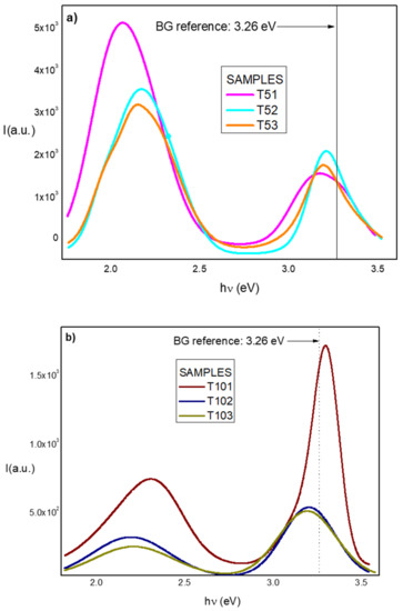
Figure 5.
PL spectra of the (a) samples series A and (b) sample series B in the UV-Visible range at room temperature. Fitting of curves were obtained with determination coefficient (R2) values higher than 99%.
In Figure 5a,b, the different shifts experienced in all spectra are illustrated. In sample series A, the BG shifts were between 60–20 meV for samples T51 and T52 respectively, i.e., towards ultraviolet range with respect to the value obtained for the ZnO reference. In sample T53, the shift was 30 meV towards the violet region. In sample series B, the BG shift of the samples T102 and T103 was towards the violet at approximately 60 meV. However, sample T101 had behaved very differently; its BG shift was towards ultraviolet reaching the value of 3.3 eV, equal to that obtained from the Tauc Plot for the reference sample, T0, and very near that of the BG standard value for ZnO at room temperature. The trend towards a decrease in the intensity of the transition from band to band (B-B) as well as the decrease in BG to around 3.2 eV and the increase in FWHM when the tellurium content increases is justified by the increase in sample defects with the increase of the dislocation density, as shown in Table 4. In addition, an overlapping of delocalized defect states with the upper part of the VB could cause a rise in the VB edge, and therefore, a decreasing BG, as was reported previously [48].
On the contrary, samples T51 and T101 show the smallest increase in their FWHM values (0.19 and 0.14 eV, respectively), being very close to the obtained value for the reference sample, T0, equal to 0.13 eV. In sample T51, this latest observation is associated with a better conservation of the ZnO crystalline quality for the lowest Te content in agreement with XRD results. With sample T101, besides the above observations, this sample reflects the highest intensity for the B-B transition comparable to the intensity of B-B transition observed in the ZnO reference, i.e., in the order of 103 arbitrary units. This means the B-B transition was more three times larger than the BG values obtained in the rest of the sample series B. Accordingly, we can consider whether, for certain average concentrations of Tellurium, it will be possible to improve the crystalline quality of the ZnOTe compound. It could be interesting to further investigate the possible size quantum effects contributing to PL emissions due to a significant diminution of the crystallite sizes in the samples with the highest Tellurium content, of which some reports already exist [49]. As an antecedent in our case, the crystallite size diminished from 20.4 nm in T0 sample to 4.9 nm in sample T101 (as illustrated in Table 4).
Different GB transitions were observed in both sample series. This band is due to the existence of local energy levels in the band gap, and the intensity variations of these transitions [50] are determined by the concentration of intrinsic defects in the ZnOTe structures. As mentioned, the GB center in the undoped sample (T0) is located about 2.32 eV, being a very intense emission (inset in Figure 4). However, in samples T52, T101, and T102, the center’s location occurs around 2.36 eV and their intensities are almost thirteen times less than that observed in sample T0. Those values are very close to 2.38 eV proposed for the center of GB [50]. B. Lin et. al. considered these emissions due to the transition from the bottom of the CB to antisite oxygen (OZn) in the BG. According to Y. M. Sun’s calculi [50], the transitions in the range from 2.19–2.23 eV can be attributed to interstitial oxygen (Oi) defects within the GB, which were observed in all samples except in T51 and T102. Nevertheless, different experiments to investigate the origin of PL bands in ZnO single crystals determined that zinc vacancies (Vzn) are responsible for maximum green emissions of samples grown in oxygen-rich atmospheres [51]. Despite the polycrystallinity of our samples, this fact is probably just as present in our results because they were grown in oxygen-rich atmosphere, and RBS results (as illustrated in Table 2) confirmed the excess of oxygen in both sample series. Other experiments are currently underway to confirm this hypothesis.
In all doped samples, it was possible to identify some transitions in the range of the lower energies, from 2.1–2.18 eV. This range encompasses the orange-yellow region of the E M S and were associated with interstitial oxygen (Oi) in the reported results on the growth of ZnO at different temperatures and enhanced in oxygen-rich atmosphere [52]. PL spectra in both sample series also show transitions corresponding to a red band (RB) in the range below 2 eV; however, these transitions are not frequently present in ZnO emissions [43] so they probably appear here as a small fraction of contaminants.
The shifts towards lower energies observed in the sample’s BG as well as the possible improvement of ZnOTe crystalline quality with Tellurium content can be very interesting sources for applications by using DC magnetron cosputtering from individual Zn and Te cathodes and improving the oxygen atmosphere control.
4. Conclusions
Two sample series of the ternary compound ZnOTe in thin films form were grown using DC magnetron cosputtering technique starting from highly pure independent zinc and tellurium targets in a controlled oxygen/argon atmosphere at room temperature. The technique used in conjunction with the experimental configuration for obtaining this type of compound and the detailed analysis of its structure and optical properties are part of this work’s novelty. The use of a constant power on the Zn cathode and two different powers on the Te cathode as well as the variation of the distance between the latter and the substrate allowed us to study the influence of these parameters on the structure, composition, and macroscopic properties of the samples. Under these conditions, the most important effect was the variable amount of Te incorporated into each sample. In that sense, different chemical compositions for each, including a homogeneous distribution of Te along their thicknesses and a variable amount of excess oxygen, were determined by RBS experiments. On the other hand, the formation of the ZnO hexagonal phase in all samples was identified by mean XRD spectra. ZnO band gap energy obtained from PL spectra was estimated at 3.26 eV, well in agreement with previously obtained values. Other highlighted results include the relative loss of ZnO crystalline quality due to the increasing Te content, and in general, a band gap energy shift towards the lowest energies, which may account for the incorporation of Te into the ZnOcrystalline network. Nevertheless, in the samples with the lowest Te content within each series (samples T51 and T101), the band gap energy values were 3.32 and 3.3 eV, respectively, almost coincident with the standard value reported (3.36 eV) for the w-ZnO phase at room temperature. This suggests the possibility of certain improvements in ZnOTe crystallinity when moderate quantities of Te are incorporated in the ZnO network. We expect there exists a critical value of the Te concentration that helps to obtain optimal effects in the formation of interbands in the BG that are of great interest for solar cell efficiency. It is a new challenge of basic research to obtain a better understanding of the physics-chemistry of ZnOTe compounds obtained through the DC magnetron cosputtering technique used here.
Author Contributions
Writing—original draft, O.S.; Writing—review & editing, M.H.-V. All authors have read and agreed to the published version of the manuscript.
Funding
This research received no external funding.
Institutional Review Board Statement
Not applicable.
Informed Consent Statement
Not applicable.
Data Availability Statement
The relevant data is contained within the article.
Acknowledgments
This work was supported by the Ministerio de Ciencia, Innovación y Universidades of Spain through the Project RTI2018-095137-B-I00. Authors acknowledge Ana Urbieta (UCM) for PL measurements, A. Climent Font for RBS measurements, and Nair López for her interesting suggestions.
Conflicts of Interest
The authors declare no conflict of interest.
References
- Lu, F.; Cai, W.; Zhang, Y. ZnO hierarchical micro/nanoarchitectures: Solvothermal synthesis and structurally enhanced photocatalytic performance. Adv. Funct. Mat. 2008, 18, 1047–1056. [Google Scholar] [CrossRef]
- Pietrzyk, M.A.; Wierzbick, A.; Zielony, E.; Pieniazek, A.; Szymon, R.; Placzek-Popko, E. Fundamental studies of ZnO nanowires with ZnCdO/ZnO multiple quantum wells grown for tunable light emitters. Sens. Actuators A 2020, 315, 112305. [Google Scholar] [CrossRef]
- Chou, H.-C.; Yang, K.-D.; Xiao, S.-H.; Patil, R.A.; Lai, C.-C.; Vincent, W.-C.; Ho, C.-H.; Liouc, Y.; Ma, Y.-R. Temperature-dependent ultraviolet photoluminescence in hierarchical Zn, ZnO and ZnO/Zn nanostructures. Nanoscale 2019, 11, 13385–13396. [Google Scholar] [CrossRef] [PubMed]
- Furuta, M.; Kamada, Y.; Kimura, M.; Shimakawa, S.-I.; Kawaharamura, T.; Wang, D.; Li, C.; Fujita, S.; Hirao, T. Photocurrent and persistent photoconductivity in zinc oxide thin-film transistors under ultraviolet-light irradiation. J. Appl. Phys. 2011, 50, 110204. [Google Scholar] [CrossRef]
- Tiginyanu, I.; Ghimpu, L.; Gröttrup, J.; Postolache, V.; Mecklenburg, M.; Stevens-Kalceff, M.A.; Ursaki, V.; Payami, N.; Feidenhansl, R.; Schulte, K.; et al. Strong light scattering and broadband (UV to IR) photoabsorption in stretchable 3D hybrid architectures based on aerographite decorated by ZnO nanocrystallites. Sci. Rep. 2016, 6, 1–11. [Google Scholar] [CrossRef]
- Postica, V.; Gröttrup, J.; Adelung, R.; Lupan, O.; Mishra, A.K.; de Leeuw, N.H.; Ababii, N.; Carreira, J.F.C.; Rodrigues, J.; Sedrine, N.B. Nanosensors: Multifunctional materials: A case study of the effects of metal doping on ZnO tetrapods with bismuth and tin oxides. Adv. Funct. Mater. 2017, 27, 1604676. [Google Scholar]
- Kim, H.; Gilmore, C.M.; Horwitz, J.S.; Piqué, A.; Murata, H.; Kushto, G.P.; Schlaf, R.; Kafafi, Z.H.; Chrisey, D.B. Transparent conducting aluminum-doped zinc oxide thin films for organic light-emitting devices. Appl. Phys. Lett. 2000, 76, 259. [Google Scholar] [CrossRef]
- Lee, S.-H.; Han, S.-H.; Jung, H.S.; Shin, H.; Lee, J.; Noh, J.-H.; Lee, S.; Cho, I.-S.; Lee, J.-K.; Kim, J.; et al. Al-doped ZnO thin film: A new transparent conducting layer for ZnO nanowire-based dye-sensitized solar cells. J. Phys. Chem. 2010, 114, 7185–7189. [Google Scholar] [CrossRef]
- Kaps, S.; Bhowmick, S.; Gröttrup, J.; Hrkac, V.; Stauffer, D.; Guo, H.; Warren, O.I.; Adam, J.; Kienle, I.; Minor, A.M.; et al. Piezoresistive response of quasi-one-dimensional ZnO nanowires using an in situ electromechanical device. ACS Omega 2017, 2, 2985–2993. [Google Scholar] [CrossRef]
- Shanmugan, N.; Suthakaran, S.; Kannadasan, N.; Kumar, K.S. Synthesis and characterization of Te doped ZnO nanosheets for photocatalytic application. J. Heterocycl. 2015, 1, 1–6. [Google Scholar]
- López, N.; Reichertz, L.A.; Yu, K.M.; Campman, K.; Walukiewicz, W. Engineering the electronic band structure for multiband solar cells. Phys. Rev. Lett. 2011, 106, 28701. [Google Scholar] [CrossRef]
- Park, S.H.; Minegishi, T.; Oh, D.C.; Chang, J.H.; Taishi, T.; Yonenaga, I.; Yao, T. P-type conductivity control of heteroepitaxially grown ZnO films by N and Te cooping and thermal annealing. J. Cryst. Growth 2013, 363, 190–194. [Google Scholar] [CrossRef]
- Tang, K.; Gu, S.L.; Wu, K.P.; Zhu, S.M.; Ye, J.D.; Zhang, R.; Zheng, Y.D. Temperature-dependent photoluminescence of ZnO films codoped with tellurium and nitrogen. J. Appl. Phys. 2012, 112, 103534. [Google Scholar] [CrossRef]
- Ozgür, Ü.; Hofstetter, D.; Morkoç, H. ZnO devices and applications: A review of current status and future prospects. Proc. IEEE 2010, 98, 1255–1268. [Google Scholar] [CrossRef]
- Walukiewicz, W.; Shan, W.; Yu, K.M.; Ager, J.W.; Haller, E.E.; Miotkowski, I.; Seong, M.J.; Alawadhi, H.; Ramdas, A.K. Interaction of localized electronic states with the conduction band: Band anticrossing in II-VI semiconductor ternaries. Phys. Rev. Lett. 2000, 85, 552. [Google Scholar] [CrossRef]
- Yu, K.M.; Walukiewicz, W.; Ager, J.W.; Bour, D.; Farshchi, R.; Dubon, D.O.; Li, S.X.; Sharp, I.D.; Haller, E.E. Multiband GaNAsP quaternary alloys. Appl. Phys. Lett. 2006, 88, 92110. [Google Scholar] [CrossRef]
- López, N.; Yu, K.M.; Tanaka, T.; Walukiewicz, W. Multicolor electroluminescence from intermediate band solar cell structures. Adv. Energy Mater. 2016, 6, 1501820. [Google Scholar] [CrossRef]
- Sonmezoglu, S.; Akman, E. Improvement of physical properties of ZnO thin films by tellurium doping. Appl. Surf. Sci. 2014, 318, 319–323. [Google Scholar] [CrossRef]
- Jamali-Sheini, F.; Yousefi, R.; Mahmoudian, M.R.; Ali, B.N.; Saaedi, A.; Huang, N.M. Facile synthesis of different morphologies of Te-doped ZnO nanostructures. Ceram. Int. 2014, 40, 7737–7743. [Google Scholar] [CrossRef]
- Sahu, R.; Dileep, K.; Negi, D.S.; Nagaraja, K.K.; Shetty, S.; Datta, R. Structural and optical property characterization of epitaxial ZnO: Te thin films grown by pulsed laser deposition. J. Cryst. Growth 2015, 410, 69–76. [Google Scholar] [CrossRef]
- Tapily, K.; Gu, D.; Boumgart, H.; Namkoong, G.; Stegall, D.; Elmustafa, A.A. Mechanical and structural characterization of atomic layer deposition-based ZnO films. Semicond. Sci. Tech. 2011, 26, 115005–115007. [Google Scholar] [CrossRef]
- Nagajurna, Y.; Hsiao, Y.-J. Au doping ZnO nanosheets sensing properties of ethanol gas prepared on MEMS device. Coatings 2020, 10, 945. [Google Scholar]
- Rana, A.H.S.; Kim, H.-S. NH4OH Treatment for an optimum morphological trade-off to hydrothermal Ga-doped n-ZnO/p-Si heterostructure characteristics. Materials 2018, 11, 37. [Google Scholar]
- Ting, M.; Yu, K.M.; Jaquez, M.; Sharp, I.D.; Ye, Y.; Sgercrantz, N.; Greif, R.; Mao, S.S.; Ping, L.C.; Walukiewicz, W. ZnO1−xTex highly mismatched alloys beyond the dilute alloy limit: Synthesis and electronic band structure. J. Appl. Phys. 2019, 125, 155702. [Google Scholar] [CrossRef]
- Singh, S.P.; Arya, S.K.; Pandey, P.; Malhotra, B.D.; Saha, S.; Sreenivas, K.; Gupta, V. Cholesterol biosensor based on rf sputtered zinc oxide nanoporous thin film. Appl. Phys. Lett. 2007, 91, 63901–63903. [Google Scholar] [CrossRef]
- Khosravi-Nejad, F.; Teimouri, M.; Jafari Marandi, S.; Shariati, M. The highly sensitive impedimetric biosensor in label free approach for hepatitis B virus DNA detection based on tellurium doped ZnO nanowires. Appl. Phys. A 2019, 125, 616. [Google Scholar] [CrossRef]
- Lee, D.U.; Kim, S.P.; Lee, K.S.; Pak, S.W.; Kim, E.K. Band gap modulation of ZnTe1-xOx alloy film by control of oxygen gas flow rate during reactive magnetron sputtering. App. Phys. Lett. 2013, 103, 263901. [Google Scholar]
- Liua, P.; Ho, C.Y.; Egbo, K.O.; Li, Z.H.; Xu, C.K.; Yu, K.M. Optoelectronic properties and doping of magnetron sputtered highly mismatched ZnO1-xTex alloy thin films. J. Alloy. Compd. 2021, 852, 156950. [Google Scholar] [CrossRef]
- Sánchez, O.; Climent, A.; Fernández Barcia, M.; Martínez Sacristán, O.; Hernández-Vélez, M. ZnO1-xTex thin films deposited by reactive magnetron co-sputtering: Composition, structure and optical properties. MRS Adv. 2017, 2, 3111–3116. [Google Scholar] [CrossRef]
- Huan-Sheng, C.; Jiayong, H.T.; Fujia, Y. Nuclear instruments and methods in physics research section B: Beam interactions with materials and atoms. Nucl. Instrum. Methods B 1993, 83, 449–453. [Google Scholar] [CrossRef]
- Mayer, M. SIMNRA User’s Guide; IPP 9/113; Max-Planck-Institut fur Plasmaphysik: Garching, Germany, 1997. [Google Scholar]
- ICDD. PCPDFWIN; 2.2 Version; International Centre for Diffraction Data: Newtown Square, PA, USA, 2001. [Google Scholar]
- Kamran, M.A. Novel low-temperature synthesis and optical properties of 1D-ZnTe nanowires. J. Sci. Adv. Mater. Dev. 2018, 3, 226–229. [Google Scholar] [CrossRef]
- Shaabana, E.R.; Kansal, I.; Mohamed, S.H.; Ferreira, J.M.F. Microstructural parameters and optical constants of ZnTe thin films with various thicknesses. Phys. B 2009, 404, 3571–3576. [Google Scholar] [CrossRef]
- Jalili, S.; Hajakbari, F.; Hojabri, A. Effect of silver thickness on structural, optical and morphological properties of nanocrystalline Ag/NiO thin films. J. Theor. Appl. Phys. 2018, 12, 15–22. [Google Scholar] [CrossRef]
- Hajakbari, F.; Shafieinejad, F. Structural, morphological, electrical, and optical properties of silver thin films of varying thickness deposited on cupric oxide. Jpn. J. Appl. Phys. 2016, 55, 35503. [Google Scholar] [CrossRef]
- Ilican, S.; Caglar, Y.; Caglar, M. Preparation and characterization of ZnO thin films deposited by sol-gel spin coating method. J. Optoelectron. Adv. Mater. 2008, 10, 2578–2583. [Google Scholar]
- Callister, W.D., Jr. Materials Science and Engineering, 4th ed.; John Wiley and Sons, Inc.: Hoboken, NJ, USA, 1997. [Google Scholar]
- Özgür, Ü.; Ya, I.A.; Liu, C.; Teke, A.; Reshchikov, M.A.; Doğan, S.; Avrutin, V.; Cho, S.-J.; Morkoç, H. A comprehensive review of ZnO materials and devices. J. Appl. Phys. 2005, 98, 41301. [Google Scholar] [CrossRef]
- Shan, F.K.; Liu, G.X.; Lee, W.J.; Lee, G.H.; Kim, I.S.; Shin, B.C. Aging effect and origin of deep-level emission in ZnO thin film deposited by pulsed laser deposition. Appl. Phys. Lett. 2005, 86, 221910. [Google Scholar] [CrossRef]
- Djurisic, A.B.; Leung, Y.H.; Tam, K.H.; Ding, L.; Ge, W.K.; Chen, H.Y.; Gwo, S. Green, yellow, and orange defect emission from ZnO nanostructures: Influence of excitation wavelength. Appl. Phys. Lett. 2006, 88, 103107. [Google Scholar] [CrossRef]
- García, P.F.; McLean, R.S.; Reilly, M.H.; Nunes, G. Transparent ZnO thin-film transistor fabricated by rf magnetron sputtering. Appl. Phys. Lett. 2003, 82, 1117. [Google Scholar]
- Mass, J.; Avella, M.; Jimenez, J.; Callahan, M.; Grant, E.; Rakes, K.; Bliss, D.; Wang, B. New Materials and Processes for Incoming Semiconductor Technologies; Dueñas, S., Castán, H., Eds.; Transworld Research Network: Kerala, India, 2006; p. 113. ISBN 81-7895-241-6. [Google Scholar]
- Kohan, A.F.; Ceder, G.; Morgan, D.; van de Walle, C.G. First-principles study of native point defects in ZnO. Phys. Rev. B 2000, 61, 15019–15022. [Google Scholar] [CrossRef]
- Chen, H.; Gu, S.; Tang, K.; Zhu, S.; Zhu, Z.; Ye, J.; Zhang, R.; Zheng, Y. Origins of green band emission in high-temperature annealed N-doped ZnO. J. Lumin. 2011, 131, 1189. [Google Scholar] [CrossRef]
- Zeng, H.; Li, Z.; Cai, W.; Liu, P. Strong localization effect in temperature dependence of violet-blue emission from ZnO nanoshells. J. Appl. Phys. 2007, 102, 104307. [Google Scholar] [CrossRef]
- Viezbicke, B.D.; Patel, S.; Davis, B.E.; Birnie, D.P. Evaluation of the Tauc method for optical absorption edge determination: ZnO thin films as a model system. Phys. Status Solidi B 2015, 252, 1700. [Google Scholar] [CrossRef]
- Wang, J.; Wang, Z.; Huang, B.; Ma, Y.; Liu, Y.; Qin, X.; Zhang, X.; Dai, Y. Oxygen vacancy induced band-gap narrowing and enhanced visible light photocatalytic activity of ZnO. ACS Appl. Mater. Interfaces 2012, 4, 4024–4030. [Google Scholar] [CrossRef]
- Studenikin, S.A.; Golego, N.; Cocivera, M. Fabrication of green and orange photoluminescent, undoped ZnO films using spray pyrolysis. J. Appl. Phys. 1998, 84, 2287. [Google Scholar] [CrossRef]
- Lin, B.; Fu, Z.; Jia, Y. Green luminescent center in undoped zinc oxide films deposited on silicon substrates. Appl. Phys. Lett. 2001, 79, 943–945. [Google Scholar] [CrossRef]
- Berseth, T.M.; Svenson, B.G.; Kusnetsov, A.Y.; Klason, P.; Zhao, Q.X.; Willander, M. Temperature-dependent photoluminescence of Li-doped ZnO. Appl. Phys. Lett. 2006, 89, 262112. [Google Scholar]
- Rodnyi, P.A.; Khodyuk, I.V. Optical and luminescence properties of zinc oxide (review). Opt. Spectrosc. 2011, 111, 776–785. [Google Scholar] [CrossRef]
Publisher’s Note: MDPI stays neutral with regard to jurisdictional claims in published maps and institutional affiliations. |
© 2021 by the authors. Licensee MDPI, Basel, Switzerland. This article is an open access article distributed under the terms and conditions of the Creative Commons Attribution (CC BY) license (https://creativecommons.org/licenses/by/4.0/).