
Effect of Ge Concentration on the On-Current Boosting of Logic P-Type MOSFET with Sigma-Shaped Source/Drain

Abstract
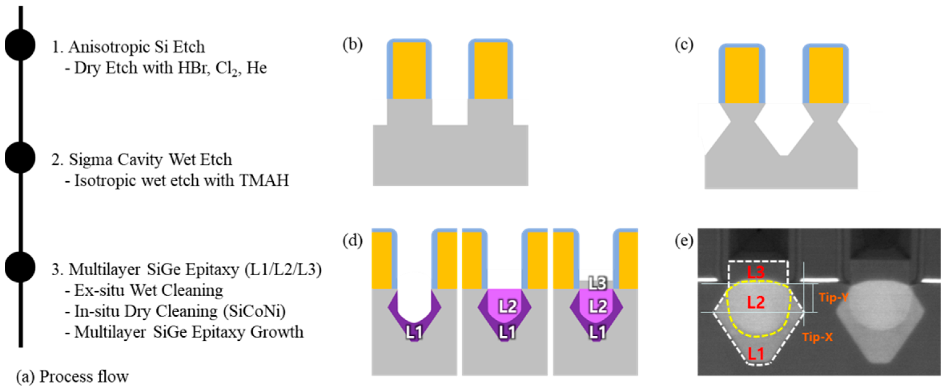
:1. Introduction
2. Materials and Methods
3. Results and Discussion
4. Conclusions
Author Contributions
Funding
Institutional Review Board Statement
Informed Consent Statement
Data Availability Statement
Conflicts of Interest
References
- Fischetti, M.V.; Laux, S.E. Band Structure, Deformation Potentials, and Carrier Mobility in Strained Si, Ge, and SiGe Alloys. J. Appl. Phys. 1996, 80, 2234–2252. [Google Scholar] [CrossRef]
- Thompson, S.E.; Armstrong, M.; Auth, C.; Alavi, M.; Buehler, M.; Chau, R.; Cea, S.; Ghani, T.; Glass, G.; Hoffman, T.; et al. A 90-Nm Logic Technology Featuring Strained-Silicon. IEEE Trans. Electron Dev. 2004, 51, 1790–1797. [Google Scholar] [CrossRef]
- Yeo, Y.-C. Enhancing CMOS Transistor Performance Using Lattice-Mismatched Materials in Source/Drain Regions. Semicond. Sci. Technol. 2007, 22, S177–S182. [Google Scholar] [CrossRef]
- Chu, M.; Sun, Y.; Aghoram, U.; Thompson, S.E. Strain: A Solution for Higher Carrier Mobility in Nanoscale MOSFETs. Annu. Rev. Mater. Res. 2009, 39, 203–229. [Google Scholar] [CrossRef]
- Bedell, S.W.; Khakifirooz, A.; Sadana, D.K. Strain Scaling for CMOS. Mrs Bull. 2014, 39, 131–137. [Google Scholar]
- Chidambaram, P.R.; Smith, B.A.; Hall, L.H.; Bu, H.; Chakravarthi, S.; Kim, Y.; Samoilov, A.V.; Kim, A.T.; Jones, P.J.; Irwin, R.B.; et al. 35% drive current improvement from recessed-SiGe drain extensions on 37 nm gate length PMOS. In Proceedings of the Digest of Technical Papers Symposium on VLSI Technology, Honolulu, HI, USA, 15–17 June 2004; p. 48. [Google Scholar]
- Ghani, T.; Armstrong, M.; Auth, C.; Bost, M.; Charvat, P.; Glass, G.; Hoffmann, T.; Johnson, K.; Kenyon, C.; Klaus, J.; et al. A 90 nm high volume manufacturing logic technology featuring novel 45 nm gate length strained silicon CMOS transistors. In Proceedings of the IEEE International Electron Devices Meeting, Washington, DC, USA, 8–10 December 2003; pp. 978–980. [Google Scholar]
- Sarangapani, P.; Weber, C.; Chang, J.; Cea, S.; Povolotskyi, M.; Klimeck, G.; Kubis, T. Atomistic Tight-Binding Study of Contact Resistivity in Si/SiGe PMOS Schottky Contacts. IEEE Trans. Nanotechnol. 2018, 17, 968–973. [Google Scholar] [CrossRef]
- Zhang, J.; Yu, H.; Schaekers, M.; Horiguchi, N.; Wang, L.-L.; Jiang, Y.-L. Observation of contact resistivity independence from schottky barrier height on heavily doped p-type SiGe. In Proceedings of the IEEE International Conference on Solid-State and Integrated Circuit Technology (ICSICT), Hangzhou, China, 25–28 October 2016. [Google Scholar]
- Sarangapani, P.; Weber, C.; Chang, J.; Cea, S.; Golizadeh-Mojarad, R.; Povolotskyi, M.; Klimeck, G.; Kubis, T. Assessment of Si/SiGe PMOS schottky contacts through atomistic tight binding simulations: Can we achieve the 10−9 Ω·cm target? In Proceedings of the 17th International Conference Nanotechnol, Pittsburgh, PA, USA, 25–28 July 2017. [Google Scholar]
- Ni, C.-N.; Rao, K.V.; Khaja, F.; Sharma, S.; Tang, S.; Chen, J.J.; Hollar, K.E.; Breil, N.; Li, X.; Jin, M.; et al. Ultra-low NMOS contact resistivity using a novel plasma-based DSS implant and laser anneal for post 7 nm nodes. In Proceedings of the 2016 IEEE Symposium on VLSI Technology, Honolulu, HI, USA, 14–16 June 2016. [Google Scholar]
- Kazi, Z.I.; Thilakan, P.; Egawa, T.; Umeno, M.; Jimbo, T. Realization of GaAs/AlGaAs Lasers on Si Substrates Using Epitaxial Lateral Overgrowth by Metalorganic Chemical Vapor Deposition. Jpn. J. Appl. Phys. 2001, 40, 4903–4906. [Google Scholar] [CrossRef]
- Hayafuji, N.; Miyashita, M.; Nishimura, T.; Kadoiwa, K.; Kumabe, H.; Murotani, T. Effect of Employing Positions of Thermal Cyclic Annealing and Strained-Layer Superlattice on Defect Reduction in GaAs-On-Si. Jpn. J. Appl. Phys. 1990, 29, 2371–2375. [Google Scholar] [CrossRef]
- Li, J.; Wang, W.; Li, Y.; Zhou, N.; Wang, G.; Kong, Z.; Fu, J.; Yin, X.; Li, C.; Wang, X.; et al. Study of Selective Isotropic Etching Si1−xGex in Process of Nanowire Transistors. J. Mater. Sci. Mater. Electron. 2020, 31, 134. [Google Scholar] [CrossRef]
- Kolahdouz, M.; Maresca, L.; Ostling, M.; Riley, D.; Wise, R.; Radamson, H.H. New Method to Calibrate the Pattern Dependency of Selective Epitaxy of SiGe Layers. Solid State Electron. 2009, 53, 858–861. [Google Scholar] [CrossRef]
- Schmidt, M.; Minamisawa, R.A.; Richter, S.; Luptak, R.; Hartmann, J.M.; Buca, D.; Zhao, Q.T.; Mantl, S. Impact of Strain and Ge Concentration on the Performance of Planar SiGe Band-to-Band-Tunneling Transistors. Ultim. Integr. Silicon 2011, 71, 42–47. [Google Scholar]
- Qin, C.; Yin, H.; Wang, G.; Hong, P.; Ma, X.; Cui, H.; Lu, Y.; Meng, L.; Yin, H.; Zhong, H.; et al. Study of Sigma-Shaped Source/Drain Recesses For Embedded-SiGe pMOSFETs. Microelectron. Eng. 2017, 181, 22–28. [Google Scholar] [CrossRef]
- Wang, G.; Luo, J.; Qin, C.; Liang, R.; Xu, Y.; Liu, J.; Li, J.; Yin, H.; Yan, J.; Zhu, H.; et al. Integration of Highly Strained SiGe in Source and Drain with HK and MG for 22 nm Bulk PMOS Transistors. Nanoscale Res. Lett. 2017, 12, 123. [Google Scholar] [CrossRef] [PubMed] [Green Version]
- Hållstedt, J.; Kolahdouz, M.; Ghandi, R.; Radamson, H.H.; Wise, R. Pattern Dependency in Selective Epitaxy of B-doped SiGe Layers for Advanced Metal Oxide Semiconductor Field Effect Transistors. J. Appl. Phys. 2008, 103, 054907. [Google Scholar] [CrossRef]
- Tokoro, K.; Uchikawa, D.; Shikida, M.; Sato, K. Anisotropic etching properties of silicon in KOH and TMAH solutions. In Proceedings of the MHA′ 98 Proceedings of the 1998 International Symposium on Micromechatronics and Human Science—Creation of New Industry, Nagoya, Japan, 25–28 November 1998; p. 65. [Google Scholar]
- Cheng, D.; Gosálvez, M.A.; Hori, T.; Sato, K.; Shikida, M. Improvement in Smoothness of Anisotropically Etched Silicon Surfaces: Effects of Surfactant and TMAH Concentrations. Sens. Actuators A 2006, 125, 415–421. [Google Scholar] [CrossRef]
- Lo, H.-C.; Peng, J.; Reis, E.; Zhu, B.; Ma, W.; Mun, S.Y.; Shintri, S.; Bazizi, E.M.; Gaire, C.; Qi, Y.; et al. A Novel Approach to Control Source/Drain Cavity Profile for Device Performance Improvement. IEEE Trans. Electron Devices 2018, 65, 3640–3645. [Google Scholar] [CrossRef]
- Loo, R.; Caymax, M.; Meunier-Beillard, P.; Peytier, I.; Holsteyns, F.; Kubicek, S.; Verheyen, P.; Lindsay, R.; Richard, O. A New Technique to Fabricate Ultra-Shallow-Junctions, Combining in Situ Vapour HCl Etching and in Situ Doped Epitaxial SiGe Re-Growth. Appl. Surf. Sci. 2004, 224, 63–67. [Google Scholar] [CrossRef]
- Kolahdouz, M.; Maresca, L.; Ghandi, R.; Khatibi, A.; Radamson, H.H. Kinetic Model of SiGe Selective Epitaxial Growth Using RPCVD Technique. J. Electrochem. Soc. 2011, 158, H457. [Google Scholar] [CrossRef]
- Radamson, H.H.; Kolahdouz, M. Selective Epitaxy Growth of Si1−xGex Layers for MOSFETs and FinFETs. J. Mater. Sci. Mater. Electron. 2015, 26, 4584. [Google Scholar] [CrossRef]
- Rosseel, E.; Profijt, H.B.; Hikavyy, A.Y.; Tolle, J.; Kubicek, S.; Mannaert, G.; L’abbe, C.; Wostyn, K.; Horiguchi, N.; Clarysse, T.; et al. Characterization of Epitaxial Si:C:P and Si:P Layers for Source/Drain Formation in Advanced Bulk FinFETs. ECS Trans. 2014, 64, 977–987. [Google Scholar] [CrossRef]
- Maeda, S.; Ko, Y.; Jeong, J.; Fukutome, H.; Kim, M.; Kim, S.; Choi, J.; Shin, D.; Oh, Y.; Lim, W.; et al. 3 Dimensional scaling extensibility on epitaxial source drain strain technology toward fin fet and beyond. In Proceedings of the 2013 Symposium on VLSI Technology, Kyoto, Japan, 11–13 June 2013. [Google Scholar]


Publisher’s Note: MDPI stays neutral with regard to jurisdictional claims in published maps and institutional affiliations. |
© 2021 by the authors. Licensee MDPI, Basel, Switzerland. This article is an open access article distributed under the terms and conditions of the Creative Commons Attribution (CC BY) license (https://creativecommons.org/licenses/by/4.0/).
Share and Cite
Ko, E.; Lee, J.; Ryu, S.-W.; Shin, H.; Park, S.; Ko, D.-H. Effect of Ge Concentration on the On-Current Boosting of Logic P-Type MOSFET with Sigma-Shaped Source/Drain. Coatings 2021, 11, 654. https://doi.org/10.3390/coatings11060654
Ko E, Lee J, Ryu S-W, Shin H, Park S, Ko D-H. Effect of Ge Concentration on the On-Current Boosting of Logic P-Type MOSFET with Sigma-Shaped Source/Drain. Coatings. 2021; 11(6):654. https://doi.org/10.3390/coatings11060654
Chicago/Turabian StyleKo, Eunjung, Juhee Lee, Seung-Wook Ryu, Hyunsu Shin, Seran Park, and Dae-Hong Ko. 2021. "Effect of Ge Concentration on the On-Current Boosting of Logic P-Type MOSFET with Sigma-Shaped Source/Drain" Coatings 11, no. 6: 654. https://doi.org/10.3390/coatings11060654