Article

The Effect of RF Sputtering Temperature Conditions on the Structural and Physical Properties of Grown SbGaN Thin Film

1
School of Engineering and Technology, Tra Vinh University, Tra Vinh 87000, Vietnam
2
Department of Materials Science and Engineering, National Taiwan University of Science and Technology, Taipei 10607, Taiwan
3
School of Basic Sciences, Tra Vinh University, Tra Vinh 87000, Vietnam
*
Authors to whom correspondence should be addressed.
Coatings 2021, 11(7), 752; https://doi.org/10.3390/coatings11070752
Submission received: 25 May 2021 / Revised: 20 June 2021 / Accepted: 21 June 2021 / Published: 23 June 2021
(This article belongs to the Special Issue Recent Advances in the Growth and Characterizations of Thin Films)

Abstract

:
By using a single ceramic SbGaN target containing a 14% Sb dopant, Sb0.14GaN films were successfully grown on n-Si(100), SiO2/Si(100), and quartz substrates by an RF reactive sputtering technology at different growth temperatures, ranging from 100 to 400 °C. As a result, the structural characteristics, and optical and electrical properties of the deposited Sb0.14GaN films were affected by the various substrate temperature conditions. By heating the temperature deposition differently, the sputtered Sb0.14GaN films had a wurtzite crystal structure with a preferential ( 10 1 ¯ 0 ) plane, and these Sb0.14GaN films experienced a structural distortion and exhibited p-type layers. At the highest depositing temperature of 400 °C, the Sb0.14GaN film had the smallest bandgap energy of 2.78 eV, and the highest hole concentration of 8.97 × 1016 cm−3, a conductivity of 2.1 Scm−1, and a high electrical mobility of 146 cm2V−1s−1. The p-Sb0.14GaN/n-Si heterojunction diode was tested at different temperatures, ranging from 25 to 150 °C. The testing data showed that the change of testing temperature affected the electrical characteristics of the diode.

Graphical Abstract

1. Introduction

It is believed that gallium nitride and its alloys are functional semiconductor materials with a crystal wurtzite structure, wide bandgap, good thermal conductivity, high carrier mobility, and a high breakdown voltage [1,2]. In the fabrication of electronics and photoelectronic components, they have been widely applied and designated as diodes and light-emitting diodes (LED), metal-oxide semiconductor field-effect transistor (MOSFET), and hetero junction field-effect transistor (HJ-FET) [3,4,5,6,7]. Overall, n- and p-type Gallium nitride films can be fabricated by many processes, such as metal organic chemical vapor deposition (MOCVD) [8,9], metal organic vapor phase epitaxy (MOVPE) [10,11], low energy electron beam irradiation (LEEBI) treatment [12], or a two flow metal organic chemical vapor deposition (TF- MOCVD) [13,14]. Besides, radio frequency (RF) sputtering technology has promising properties in application, as it is more inexpensive, uncomplicated to clean, and easy to use with various sputtering conditions. Using this technique, the target can be designed according to a wide range of compositions. It is reasonable to study the doping in III–nitride compound semiconductors, and a GaN film has been easily fabricated. Recently, our group has accomplished a deposited p-GaN and n-GaN film [15,16,17]. In a previous experiment, we had studied the effects of an Sb dopant on the semiconductor characteristics of Sb-x-GaN films sputtered by RF reactive sputtering technology using a single ceramic Sb-x-GaN target with an Sb dopant at x = 0.0, 0.07, 0.14, and 0.2. The results determined that these deposited Sb-x-GaN films converted to a p-semiconductor at x= 0.07, 0.14, and 0.2. The p-SbGaN/n-Si(100) heterojunction diodes performed successfully and their electrical characteristics at room temperature were thoroughly investigated [18] In 2019, our previous work was performed in conditions that affected the electrical, optical, and structural properties of the GeGaN thin films grown using RF reactive sputtering [19]. At the highest temperature of 400 °C, the Ge0.07GaN film acted as an n-semiconductor, had a smaller bandgap energy of 3.02 eV, and achieved a higher carrier concentration of 1.30 × 1018 cm−3, an electrical conductivity of 1.46 Scm−1, and an electron mobility of 7 cm2V−1s−1. However, the influences of the different heating substrate temperature conditions on the characteristics of Sb-GaN thin films have not been studied by many researchers until this work. In this work, we studied the influences of different deposition temperatures on the structural, optical, and electrical characteristics of the Sb0.14GaN films and the characteristics of the p-Sb0.14GaN/n-Si heterojunction diode at different testing temperatures. Firstly, Sb0.14GaN thin films were deposited at various substrate heating temperatures, of 100, 200, 300, and 400 °C. Secondly, a diode was fabricated by growing the p-Sb0.14GaN film on an n-Si substrate with the electrodes on the top using modeling by RF sputtering, then the electrical characteristics of the diode were thoroughly investigated at various working temperatures, from 25 to 150 °C.

2. Experimental Details

To thoroughly investigate the effects of different heating substrate temperature conditions on the deposited Sb doped GaN film, the SbGaN ceramic target was prepared with Sb/(Sb+Ga) at a molar ratio of 14 at% and named Sb0.14GaN target. Using a single Sb0.14GaN target for deposition, the Sb0.14GaN films were successfully fabricated on n-type Si(100), SiO2/Si(100), and quartz substrates by RF sputtering. The Sb0.14GaN films sputtered on the n-Si(100) substrates at different temperatures were used to study crystal structure properties, morphological and topographical surfaces, and analyzing the composition of the Sb0.14GaN films. To test the electrical properties of the films, the Sb0.14GaN films were deposited on an SiO2/Si(100) substrate using the RF technique at various temperature ranges, 100–400 °C. Additionally, the Sb0.14GaN films grown on quartz substrates at different heating substrate temperatures were used to investigate the optical properties of Sb0.14GaN films. The n-Si(100) substrates used in this work possessed an electrical mobility of ~200 cm2V−1s−1, an electron concentration of ~1015cm−3, an electrical resistivity of ~1–10 Ωcm, a diameter of 2 inches, and a thickness of ~550. In order to study the effects of deposition temperature on the SbGaN film properties, the Sb0.14GaN films were sputtered at substrate temperature conditions of 100, 200, 300, and 400 °C, output RF sputtering power was constant, at 120 W, and deposition time was kept at 30 min. Before depositing, the pressure of the working chamber was lowered to 1 × 10⁻⁶ Torr by the mechanical and diffusion pumps. For depositing, the reactive RF sputtering was fixed at a working pressure of 9 × 10⁻³ Torr and a gas mixture of Ar and N2 flowed at rates of 5 sccm and 15 sccm, respectively. In this experiment, the target was located opposite the substrate at a distanced of 5 cm in the working chamber. The heterojunction diode successfully performed the reactive RF sputtering technology, and the heterojunction diode created a sputtered p-type Sb-0.14-GaN film on the n-Si substrate [18]. The heterojunction p-Sb0.14GaN/n-Si(100) diode was made by sputtering an Sb0.14GaN film on an n-Si(100) substrate. The diode structure was designed in a top-top electrode model fabricated by depositing Sb0.14GaN film on the n-Si substrate. It is known that metals with a high work function (such as Pt, Mo, Ni, etc.) have often been applied to form Schottky contacts with an n-type semiconductor, and ohmic contacts with a p-type semiconductor in the modeling of metal-oxide-semiconductor MOS, metal-semiconductor MS, homo-, or heterojunction diodes. Besides, metals with a low work-function (such as Al, Ag, etc.) have often been employed to fabricate ohmic contacts with n-type semiconductors, and Schottky contacts with a p-type semiconductor. In this work, the modeling of Pt/p-Sb0.14GaN/n-Si/Al was applied to Al to make an ohmic contact with n-Si and Pt to perform an ohmic contact with p-Sb-GaN. The commercially purchased Al and Pt targets (99.999%) were applied to the electrodes at a sputtering temperature of 200 °C for 30 min, on the top of the film. The physical methods for designing and operating the diodes with our sputtered III-nitride thin films are particularly described in our previous works [7,15,18,20,21,22]. To study the influence of the testing conditions on the diode, the p-Sb0.14GaN/n-Si(100) diode was deployed in current–voltage tests at various testing temperatures, ranging from 25 to 150 °C.
The crystalline structure of the Sb0.14GaN films was studied by X–ray diffractometry (XRD, D8 Discover, Bruker, Billerica, MA, USA). Scanning electron microscopy (SEM, JSM–6500F, JEOL, Tokyo, Japan) was applied to investigate the morphological surface and cross-section images of the Sb0.14GaN films. The topographical surface and the film roughness formed by the root-mean-square (rms) value were computed by atomic force microscopy (AFM, Dimension Icon, Bruker, MA, USA). Compositional analyses of the Sb0.14GaN films were performed by the energy dispersive spectrometer (EDS, JSM–6500F, JEOL, Tokyo, Japan) supported on SEM. The absorption spectra of the Sb0.14GaN films were tested using an ultraviolet-visible (UV–Vis) spectrometer (V-670, Jasco, Tokyo, Japan), and a Hall measurement system (HMS–2000, Ecopia, Tokyo, Japan) was used to determine the electrical properties of the Sb0.14GaN films, consisting of hole concentration, electrical mobility, and conductivity with a maximum magnetic field of 0.51 T. A semiconductor device analyzer (Agilent, B1500A, Santa Clara, CA, USA) was used to study the electrical characteristics of the p-Sb0.14GaN/n-Si(100) heterojunction diode at a temperature range of 25 to 150 °C.

3. Results and Discussion

3.1. Effects of Growth Temperature on the Deposited SbGaN Film Properties

The compositional films of these sputtered Sb0.14GaN films, grown at different temperatures in the range of 100–400 °C, were studied by the energy dispersive spectrometer supported by a SEM. Table 1 presents the EDS compositional data of the Sb0.14GaN films deposited at heating substrate ranges of 100–400 °C. As Ga concentration in the Sb0.14GaN films grown at different heating substrate temperatures, from 100 to 400 °C, was a decreasing trend, the concentration of Sb in these films increased. There was a slight reduction in Ga concentration in the Sb0.14GaN films, listed as 46.48, 46.31, 45.89, and 45.64 at% corresponding to substrate temperature conditions of 100, 200, 300, and 400 °C, respectively. Sb concentration in the Sb0.14GaN films deposited at 100–400 °C increased by 3.24, 3.91, 4.92, and 5.23 at%, respectively. Thus, the [Sb]/([Ga]+[Sb) molar ratios were 0.065, 0.078, 0.097 and 0.103 for the Sb0.14GaN films at 100, 200, 300 and 400 °C, respectively. The Sb molar ratio of the sputtered Sb0.14GaN films increased significantly as the temperature of the heating substrate increased. As the [N]/([Ga]+[Sb]) ratio of the Sb0.14GaN film at 100 °C was 1.011, the [N]/([Ga]+[Sb]) ratio of the Sb0.14GaN films deposited at 200, 300 and 400 °C were 0.991, 0.968 and 0.966, which indicated that these Sb0.14GaN films had a slight nitrogen vacancy and their electrical properties could be determined by film’s deficient nitrogen state. It is expected that the different temperatures of the heating substrates can explain the changes in the film properties. The morphological surfaces and cross-section patterns of Sb0.14GaN films grown by an RF reactive sputtering system at deposition temperatures ranging from 100 to 400 °C were figured by scanning electron microscopy. Figure 1 displays images of the SEM surface and cross sectional patterns of the Sb0.14GaN films deposited at a sputtering temperature in the range of 100–400 °C, with power maintained at 120 W. The surface SEM images showed that the Sb0.14GaN films at different heating-substrate temperatures had a continuous microstructure, film smoothness, and medium grain size in the nanometer. From the inserted cross-sectioning SEM figures in Figure 1, it can be seen that these Sb0.14GaN films adhered well and had good interfaces, without cracks and voids between the Sb0.14GaN layers and n-Si substrate. As shown in Table 2, these Sb0.14GaN films exhibited thicknesses of 1.0, 1.13, 1.17, and 1.24 µm as the heating substrate temperatures of the sputtering process were maintained at 100, 200, 300, and 400 °C, respectively. As a result, there was an incremental growth rate of 33.33, 37.67, 39.00, and 41.33 nm/min, corresponding to each sputtering temperature of the deposition system. The physical phenomenon could indicate that more Ar hit the Sb0.14GaN target; a higher heating substrate temperature condition corresponds to a faster sputtering rate. Additionally, Table 3 displays the sizes of wurtzite crystalline, computed by the Scherer equation from the investigated XRD data. They were found to be 24, 24, 22, and 18 nm for the Sb-014-GaN films deposited at temperatures of 100, 200, 300, and 400 °C, respectively.
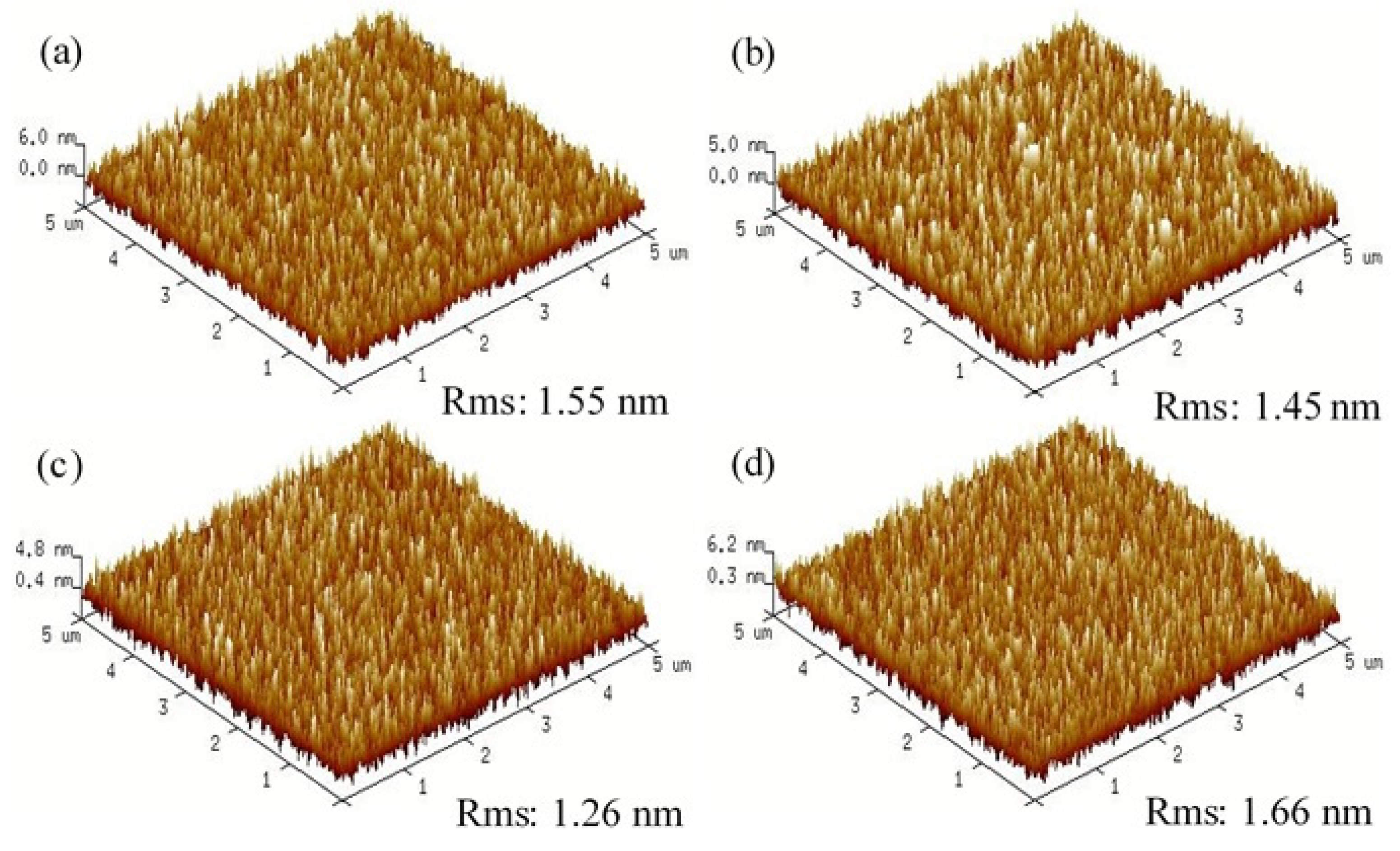
The topographical surface and the root mean square (rms) roughness values of the Sb0.14GaN films deposited at 100, 200, 300, and 400 °C were studied by atomic force microscopy (AFM). Figure 2 presents the AFM morphologies of the Sb0.14GaN films after scanning dimensions of 5 × 5 µm2. The roughness values of the Sb0.14GaN films were 1.55, 1.45, 1.26, and 1.66 nm, of the Sb0.14GaN films deposited at heating substrate temperatures of 100, 200, 300, and 400 °C, respectively. The GaN film sputtered using a radio frequency (RF) sputtering technique had a film roughness ranging from 0.7 to 20 nm [23], while the GaN films made with a MOCVD system had various degrees of film roughness, ranging from 0.5 to 3 nm [24]. Regarding the morphological and topographical surfaces and EDS compositional analyses of the grown Sb0.14GaN films, each exhibited a smooth surface and an increase in the growth rate from 33.33 to 41.33 nm/min, as the heating temperature substrate rose. It is reasonable to infer that the faster depositing of the sputtering system was formed by the strong bombardment of argon onto the Sb0.14GaN target at a higher RF sputtering temperature.
Figure 3 presents the XRD spectra of the Sb0.14GaN films deposited by RF reactive sputtering at various deposition temperatures, from 100 to 400 °C, and fixed at 120 W under an Ar/N2 gas atmosphere. From the XRD, all the Sb0.14GaN films grown on the n-Si(100) substrates, whether heating substrate temperature conditions applied for the sputtering processes were 100, 200, 300, and 400 °C, had a wurtzite structure and were polycrystalline. The ( 10 1 ¯ 0 ), ( 10 1 ¯ 1 ), ( 11 2 ¯ 0 ), and ( 11 2 ¯ 2 ) peaks of diffraction were determined from those Sb0.14GaN films containing a growth plane with a ( 10 1 ¯ 0 ) dominating peak; another second peak was not identified from the XRD images. At the higher sputtering temperature conditions, there was a slight shift in the position of the dominatant ( 10 1 ¯ 0 ) peak, to a higher 2θ angle. From the tested XRD data at a 2θ angle, the positions of diffraction ( 10 1 ¯ 0 ) peaks were discovered at 32.15°, 32.15°, 32.20°, and 32.26° on the Sb0.14GaN films grown at the substrate temperature conditions of 100, 200, 300, and 400 °C, respectively. Table 2 presents the statistics from the XRD analysis. The lattice constants of a, c, and the volume of the unit cell of the Sb0.14GaN films grown at various growth temperatures from 100 to 400 °C are shown in Table 2. The data displays that there was a slight decrease in the lattice constant of c from 5.23, 5.23, 5.22 to 5.21 Å and a from 3.212, 3.212, 3.21 to 3.20 Å for the Sb0.14GaN films fabricated at heating growth temperatures of 100, 200, 300 and 400 °C, respectively. Besides, the Sb0.14GaN films grown at 100, 200, 300, and 400 °C had cell volumes listed as 46.70, 46.69, 46.58, and 46.23 Å3, respectively. As the Sb0.14GaN films were made at different RF sputtering temperatures, ranging from 100 to 400 °C, the full width at half maxima (FWHM) values of the ( 10 1 ¯ 0 ) peaks experienced a slight increment of 0.37, 0.38, 0.42, and 0.51°, respectively. By using the Scherer equation for computing crystalline size and the XRD parameters presented in Table 2, the size of the crystallites was substantially smaller at higher heating temperatures, estimated to be 24, 24, 22, and 18 nm for the Sb0.14GaN films grown at 100, 200, 300, and 400 °C, respectively. It was determined that the different depositing temperatures possibly affected the crystalline structure, as the Sb0.14GaN films were grown at deposition temperatures of 100, 200, 300, and 400 °C. In sputtering conditions at a higher heating temperature, there was an increase in the Sb content in the as-sputtered Sb0.14GaN films that exhibited a smaller crystallite size and distortion in the crystal structure.
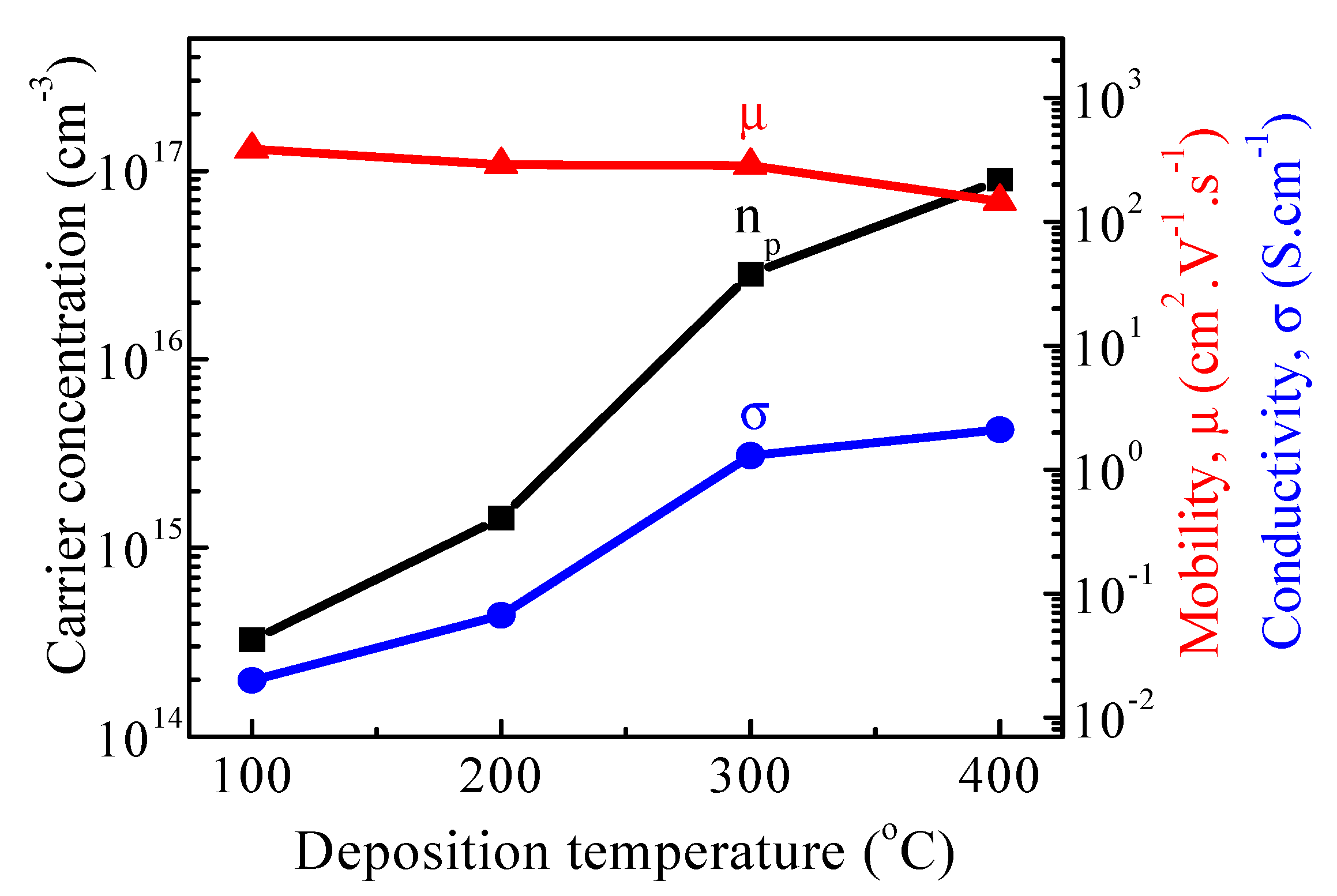
The Hall measurement system was used to measure the electrical characteristics of the RF sputtered Sb0.14GaN films at various temperature depositions, from 100 to 400 °C. All of these Sb0.14GaN films retained p-semiconductor layers, and the electrical parameters, named bulk concentration, mobility, and conductivity, of the Sb0.14GaN films are detailed in Figure 4. The hole concentration and electrical mobility of the Sb0.14GaN films grown at various heating substrate temperatures of 100, 200, 300, and 400 °C shown in Table 4 showed a significant increase, from 3.25 × 1014 cm−3 and 385 cm2V−1s−1, 1.44 × 1015 cm−3 and 289 cm2V−1s−1, 2.83 × 1016 cm−3 and 287 cm2V−1s−1, to 8.97 × 1016 cm−3 and 146 cm2V−1s−1, respectively. This is explained by the fact that the highest Sb content of 10.3 at % appeared in the composition of the Sb0.14GaN film grown at the highest sputtering temperature of 400 °C, correlating to the highest film hole concentration. From the experimental data in Table 4, it is supposed that the hole conductivity of a film could be calculated using hole concentration and mobility, as the Sb0.14GaN grown at the different deposition temperatures of 100, 200, 300 and 400 °C achieved an increment of electrical conductivity, from 0.02, 0.067, and 1.3 to 2.1 Scm−1, respectively. This indicates that the electrical properties of these sputtered Sb0.14GaN films were affected by the different depositing temperature conditions.
The optical properties of the Sb0.14GaN films grown at different temperature depositions, from 100 to 400 °C, were measured using a UV–Vis system at room temperature. From the UV—Vis analysis data, the coefficient of optical absorption and bandgap energy, Eg, of the Sb0.14GaN films could be estimated by employing the Tauc equation expressed following Equation (1):
( αhν ) 2 = A ( h ν E g )
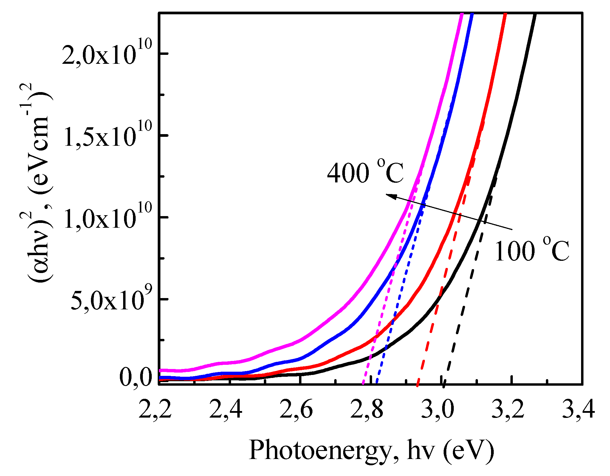
where α is physical quantity as a coefficient of optical absorption, A is a constant, hv is the energy value of the incident photon, and Eg is the bandgap energy of the Sb0.14GaN films deposited at the different growth temperatures. The plots of the (αhν)2-hν curves and the bandgap energy of the Sb0.14GaN films grown at different heating substrate temperatures are shown in Figure 5. The bandgap, Eg, from the extrapolated curves were 3.01, 2.93, 2.81, and 2.78 eV for the Sb0.14GaN films deposited at different temperature depositions from 100 to 400 °C, respectively. In the experiment, the Sb content of the Sb0.14GaN films increased from 3.24 at% at a depositing temperature of 100 °C, to the highest Sb content value of 5.23% at the substrate temperature of 400 °C; thus, their bandgap Eg decreased from 3.01 to 2.78 eV. K. M. Yu et al. presented that GaN1−xSbx alloys could modify the site of absorption from 3.4 eV (GaN) to close to 1 eV for alloys composed of higher than 30 at% Sb [25]. Neugebauer et al. illustrated that the smallest formation of energy remained in p-GaN in the state of vacancy-nitrogen (a donor), and in the n-GaN of an vacancy-gallium state (an acceptor) [26]. Mattila clearly confirmed a sophisticated formation between donors of positively charged and negatively charged cation vacancies [27]. As the Sb0.14GaN thin films were sputtered at different temperature depositions, from 100 to 400 °C, there was smaller absorption energy and lower defect levels caused by presenting the solid Sb solution into the GaN, and Sb formed as an acceptor in the GaN.

3.2. The p-Sb0.14GaN/n-Si heterojunction Diode

In our previous work, we have successfully tested the I–V characteristics of the p-Sb0.14GaN/n-Si(100) heterojunction diode at room temperature by using the RF sputtering technique [18]. In this experiment, the p-Sb0.14GaN/n-Si(100) diode was investigated at various testing temperatures, ranging from 25 to 150 °C. Figure 6 presents the current density and voltage characteristic of the p-Sb0.14GaN/n-Si diode tested at the different temperature ranges of 25–150 °C. The p-Sb0.14GaN/n-Si(100) diode was tested at a range of voltages from −20 to +20 V, and applied at the different working temperatures of 25, 75, 100, 125, and 150 °C. As listed in Table 5, the leakage currents of this diode were 5.13 × 10⁻⁵, 1.26 × 10⁻⁴, 5.98 × 10⁻⁴, 1.53 × 10⁻², and 2.96 × 10⁻² Acm−2 at the reverse bias of −5 V, respectively. The J–V curves in Figure 6 present that the p-Sb0.14GaN/n-Si diode at a working temperature range 25–150 °C had the same turnon voltages at 1.25 V, while the diode experienced breakdown voltages at 20 V. There was a relationship between the current density of the diode and testing temperature. As the testing temperature rose from 25, 75, 100, 125 to 150 °C at the forward bias of 20 V, the current density of the p-Sb0.14GaN/n-Si diode increased from 0.139, 0.461, 0.663, 0.886 to 1.34 A/cm2, respectively. It is supposed that the electrical properties of the sputtered p-type Sb0.14GaN at different heating substrate temperatures presented in Figure 4 applied to the changes in leakage current density and forward current density values of the diode in Figure 6 and Figure 7.
By applying a standard thermionic-emission (TE) model displayed in the below Equation (2), the electrical properties of the diode can be calculated as qV > 3 kT [6,11,28]:
I = I 0 exp [ q nKT ( V IR s ) ]
where q is the carrier charge (1.60 × 10⁻¹⁹ C), V is the applied voltage, I0 is the value of the saturation current, n is the ideality factor, I0 the saturation current, the series resistance is named Rs, K displays the Boltzmann constant (1.38 × 10⁻²³ JK−1), and T is the investigating temperature in Kelvin. With the loop of lnI versus V figured by using Equation (2), the intersection of the interpolated straight line from the linear region of the semilog chart determined that the saturation current (I0) of the diode can be given by the intersection of the interpolated straight line from the linear region of the semilog chart. The Io values were 7.60 × 10⁻⁵, 1.7 × 10⁻⁴, 3.3 × 10⁻⁴, 5.6 × 10⁻⁴, and 1.3 × 10⁻³ A for the p-Sb0.14GaN/n-Si diode at a testing temperature ranging from 25 to 150 °C. Additionally, ϕB, the barrier height, and n, the ideality factor, can be calculated from the retrieved I0 data by applying Equations (3) and (4) [15,17,28].
Figure 6 also determined the electrical characteristics of the p-Sb0.14GaN/n-Si diode tested at different working temperatures. From the data for various investigating temperatures of 25, 75, 100, 125, and 150 °C in Table 5, the ideality factor n can be figured to be 5.6, 4.0, 4.76, 5.31, and 5.71. In addition, by testing within the temperature range of 25–150 °C, ϕB the barrier height can be computed to be greater than the values estimated in Figure 7, e.g., 0.45, 0.58, 0.56, 0.54, and 0.52 eV, respectively.
ϕ B = KT q ln ( AA * T 2 I o )
n = ( q KT ) × ( dV d ( lnI ) )
By using Cheungs’ method presented in Equation (5), the Rs series resistance and n, ideality factor, were calculated for the p-Sb0.14GaN/n-Si diode worked at the different temperatures and shown in Figure 8 [17,28,29,30]. The n ideality factors were found to be 5.59, 3.93, 4.78, 5.36, and 5.74. The RS series resistances were 7.51, 6.72, 1.37, 0.53, and 0.38 kΩ for the testing temperatures of 25, 75, 100, 125, and 150 °C, respectively (Table 5).
( dV d ( lnI ) ) = nKT q + IR s
From the surveyed data, it can be seen that as the heating substrate temperature of the sputtering process increases, the Sb0.14GaN film possessed more electrical conductivity (σ) and carrier concentration (ne), as shown in Table 4. This means that the Sb0.14GaN device had a higher leakage current density and forward current density at higher testing temperatures.
At this time, there is no report on the SbGaN/Si heterojunction device. Our diode showed an excellent breakdown voltage of 20 V compared with some devices based on GaN and its alloys, which often display breakdown voltages of ~ 13V [30,31,32,33,34]. Similar results were also determined in the investigation of heterojunction diodes with different approaches. Mohd Yusoff et al. studied the pn junction diode based on GaN grown on Si(111) substrate at room temperature (RT). Their ideality factors (n) decreased from 15.14 to 19.68, with an increase in the testing temperature within the range of 30–104 °C [35]. Chirakkara et al. fabricated a n–ZnO/p–Si(100) hetero diode by pulsed laser deposition. Their barrier heights increased from 0.6 eV (at 300 K) to 0.76 eV (at 390 K) when testing at various temperatures, ranging from 300 to 390 K [36]. Lin et al. reported leakage current densities of 6.65×10⁻⁷ A/cm2 at a reverse voltage of 5 V and a large turn-on voltage of 9.2 V, which was measured for I–V curves in the sputtered-n-Al0.05In 0.075GaN/p-Si heterodiode. In another work, they also identified a turnon voltage of 2.70 V in the sputtered n-Al0.075In0.25GaN/p-Si diode when testing at RT [37,38].
In addition, although the reported III–V diodes made by MOCVD displayed the epitaxial growth of their semiconductors, their deposition was conducted at high temperatures of 900 °C for GaN [9,10,28]. The p-Sb0.14GaN/n-Si diodes had shown the special properties shown in the IV measurements, which could be attributed to the low temperature process only at 400 °C. Our diode with stable electrical properties up to test temperatures of 150 °C has great potential for application in power diodes and electronic devices.

4. Conclusions

Sb0.14GaN films were successfully fabricated on n-type Si(100) substrates by applying radio frequency (RF) reactive sputtering technology at various heating substrate temperatures, from 100 to 400 °C. The investigated data indicated that all the Sb0.14GaN films retained the structure of the polycrystalline and electrical conductivity at the different depositing temperature conditions. At the various sputtering temperatures of the deposition process, the Sb0.14GaN films were affected by the film properties and experienced a significant structural distortion. At the highest heating substrate temperature of 400 °C, the Sb0.14GaN film behaved as a p-semiconductor layer and had the highest bulk hole concentration and electrical conductivity, of 8.97 × 1016 cm−3, and 2.1 Scm−1, respectively. The electrical characteristics of the p-Sb0.14GaN layer/n-Si substrate diode were measured and computed at the different testing temperature ranges of 25–150 °C using semiconductor device analyzer. These results proved that the testing temperature conditions affected the electrical characteristics of the p-Sb0.14GaN/n-Si device. Forward bias analysis at 20 V revealed the highest current density of 1.34 A/cm2 to be for the diode operating at 150 °C and it is believed that there is a relationship between a working temperature decrement of 125, 100, 75, and 25 °C and a significant current density decrease from 0.886, 0.663, 0.461 to 0.139 A/cm2, respectively.

Author Contributions

Data curation: C.P.T. and T.T.A.T.; methodology: C.P.T. and T.T.A.T.; writing—original draft and investigation: C.P.T. and T.T.A.T.; formal analysis, funding acquisition and writing—review & editing: C.P.T., T.T.A.T.; supervision: D.-H.K. All authors have read and agreed to the published version of the manuscript.

Funding

This research received no external funding.

Institutional Review Board Statement

Not Applicable.

Informed Consent Statement

Not Applicable.

Data Availability Statement

Data is contained within the article or supplementary material.

Acknowledgments

This work was supported by the Ministry of Science and Technology of the Republic of China under grant numbers 109-2222-E-011-006.

Conflicts of Interest

The authors declare no conflict of interest.

References

  1. Akasaki, I.; Amano, H. Crystal Growth and Conductivity Control of Group III Nitride Semiconductors and Their Application to Short Wavelength Light Emitters. Jpn. J. Appl. Phys. 1997, 36, 5393–5408. [Google Scholar] [CrossRef]
  2. Jain, S.C.; Willander, M.; Narayan, J.; Overstraeten, R.V. III-nitrides-Growth, characterization, and properties. J. Appl. Phys. 2000, 87, 965–1006. [Google Scholar] [CrossRef] [Green Version]
  3. Fujii, T.; Gao, Y.; Sharma, R.; Hu, E.L.; DenBaars, S.P.; Nakamura, S. Increase in the extraction efficiency of GaN-based light-emitting diodes via surface roughening. Appl. Phys. Lett. 2004, 84, 855–857. [Google Scholar] [CrossRef]
  4. Pearton, S.J.; Ren, F.; Zhang, A.P.; Lee, K.P. Fabrication and performance of GaN electronic devices. Mater. Sci. Eng. R Rep. 2000, 30, 205–212. [Google Scholar] [CrossRef]
  5. Rajan, S.; Chini, A.; Wong, M.H.; Speck, J.S.; Mishra, U.K. N-polar GaN/AlGaN/GaN high electron mobility transistors. J.Appl. Phys. 2007, 102, 044501. [Google Scholar] [CrossRef] [Green Version]
  6. Tuan, T.T.A.; Kuo, D.-H.; Li, C.C.; Yen, W.-C. Schottky barrier characteristics of Pt contacts to all sputtering-made n-type GaN and MOS diodes. J. Mater. Sci. Mater. Electron. 2014, 25, 3264–3270. [Google Scholar] [CrossRef]
  7. Tuan, T.T.A.; Kuo, D.-H.; Saragih, A.D.; Li, G.-Z. Electrical properties of RF-sputtered Zn-doped GaN films and p-Zn-GaN/n-Si hetero junction diode with low leakage current of 10−9A and a high rectification ratio above 105. Mater. Sci. Eng. B 2017, 222, 18–25. [Google Scholar] [CrossRef]
  8. Shuji, N. GaN Growth Using GaN Buffer Layer. Jpn. J. Appl. Phys. 1991, 30, L1705. [Google Scholar]
  9. Guarneros, C.; Sánchez, V. Magnesium doped GaN grown by MOCVD. Mater. Sci. Eng. B. 2010, 174, 263–265. [Google Scholar] [CrossRef]
  10. Akasaki, I.; Amano, H.; Koide, Y.; Hiramatsu, K.; Sawaki, N. Effects of ain buffer layer on crystallographic structure and on electrical and optical properties of GaN and Ga1-xAlxN (0 < x < 0.4) films grown on sapphire substrate by MOVPE. J. Crystal. Growth. 1989, 98, 209–219. [Google Scholar]
  11. Shota, K.; Kazumasa, H.; Nobuhiko, S. Fabrication of GaN Hexagonal Pyramids on Dot-Patterned GaN/Sapphire Substrates via Selective Metalorganic Vapor Phase Epitaxy. Jpn. J. Appl. Phys. 1995, 34, L1184. [Google Scholar]
  12. Hiroshi, A.; Masahiro, K.; Kazumasa, H.; Isamu, A. P-type Conduction in Mg-Doped GaN Treated with Low-Energy Electron Beam Irradiation (LEEBI). Japan. J. Appl. Phys. 1989, 28, L2112. [Google Scholar]
  13. Nakamura, S.; Harada, Y.; Seno, M. Novel metalorganic chemical vapor deposition system for GaN growth. Appl. Phys. Lett. 1991, 58, 2021–2023. [Google Scholar] [CrossRef]
  14. Shuji, N.; Takashi, M.; Masayuki, S.; Naruhito, I. Thermal Annealing Effects on P-Type Mg-Doped GaN Films. Jpn. J. Appl. Phys. 1992, 31, L139. [Google Scholar]
  15. Li, C.-C.; Kuo, D.-H. Material and technology developments of the totally sputtering-made p/n GaN diodes for cost-effective power electronics. J. Mater. Sci. Mater. Electron. 2014, 25, 1942–1948. [Google Scholar] [CrossRef]
  16. Thao, C.P.; Kuo, D.H. Electrical and structural characteristics of Ge-doped GaN thin films and its hetero-junction diode made all by RF reactive sputtering. Mater. Sci. Semicond. Process 2018, 74, 336–341. [Google Scholar] [CrossRef]
  17. Kuo, D.H.; Tuan, T.T.A.; Li, C.C.; Yen, W.C. Electrical and structural properties of Mg-doped InxGa1−xN (x ≤ 0.1) and p-InGaN/n-GaN junction diode made all by RF reactive sputtering. Mater. Sci. Eng. B 2015, 193, 18–25. [Google Scholar] [CrossRef]
  18. Thao, C.P.; Tuan, T.T.A.; Kuo, D.H.; Ke, W.C. Reactively Sputtered Sb-GaN Films and its Hetero-Junction Diode: The Exploration of the n-to-p Transition. Coatings 2020, 10, 210. [Google Scholar] [CrossRef] [Green Version]
  19. Thao, C.P.; Kuo, D.H.; Tuan, T.T.A.; Tuan, K.A.; Vu, N.H.; Via Sa Na, T.T.; Nhut, K.V.; Sau, N.V. The Effect of RF Sputtering Conditions on the Physical Characteristics of Deposited GeGaN Thin Film. Coatings 2019, 9, 645. [Google Scholar] [CrossRef] [Green Version]
  20. Li, C.C.; Kuo, D.H. Effects of growth temperature on electrical and structural properties of sputtered GaN films with a cermet target. J. Matter. Sci Mater. Electron. 2014, 25, 1404–1409. [Google Scholar] [CrossRef]
  21. Tuan, T.T.A.; Kuo, D.H. Characteristics of RF reactive sputter-deposited Pt/SiO2/n-InGaN MOS Schottky diodes. Mater. Sci. Semicond Process 2015, 30, 314–320. [Google Scholar] [CrossRef]
  22. Li, C.C.; Kuo, D.H.; Hsieh, P.W.; Huang, Y.S. Thick InxGa1−x N Films Prepared by Reactive Sputtering with Single Cermet Targets. J. Electron. Mater. 2013, 42, 2445–2449. [Google Scholar] [CrossRef]
  23. Kim, H.W.; Kim, N.H. Preparation of GaN films on ZnO buffer layers by RF magnetron sputtering. Appl. Sur. Sci. 2004, 236, 192–197. [Google Scholar] [CrossRef]
  24. Chyr, I.; Lee, B.; Chao, L.C.; Steckl, A.J. Damage generation and removal in the Ga+ focused ion beam micromachining of GaN for photonic applications. J. Vacuum. Sci. Tech. B 1999, 17, 3063–3067. [Google Scholar] [CrossRef]
  25. Yu, K.M.; Sarney, W.L.; Novikov, S.V.; Segercrantz, N.; Ting, M.; Shaw, M.; Svensson, S.P.; Martin, R.W.; Walukiewicz, W.; Foxon, C.T. Highly mismatched GaN1-xSbx alloys: Synthesis, structure and electronic properties. Semicond. Sci. Tech. 2016, 31, 083001. [Google Scholar] [CrossRef] [Green Version]
  26. Neugebauer, J.; Van de Walle, C.G. Atomic geometry and electronic structure of native defects in GaN. Phys. Rev. B 1994, 50, 8067–8070. [Google Scholar] [CrossRef] [PubMed]
  27. Mattila, T.; Nieminen, R.M. Point-defect complexes and broadband luminescence in GaN and AlN. Phys. Rev. B 1997, 55, 9571–9576. [Google Scholar] [CrossRef] [Green Version]
  28. Reddy, V.R.; Prasanna, B.P.; Padma, R. Electrical Properties of Rapidly Annealed Ir and Ir/Au Schottky Contacts on n-Type InGaN. J. Metall. 2012, 1, 1–9. [Google Scholar] [CrossRef] [Green Version]
  29. Cheung, S.K.; Cheung, N.W. Extraction of Schottky diode parameters from forward current-voltage characteristics. Appl. Phys. Lett. 1986, 49, 85–87. [Google Scholar] [CrossRef]
  30. Padma, R.; Reddy, V.R. Electrical Properties of Ir/n-InGaN/Ti/Al Schottky Barrier Diode in a Wide Temperature Range. Adv. Mater. Lett. 2014, 5, 31–38. [Google Scholar] [CrossRef]
  31. Lee, S.Y.; Kim, T.H.; Suh, D.I.; Park, J.E. An electrical characterization of a hetero-junction nanowire (NW) PN diode (n-GaN NW/pSi) formed by dielectrophoresis alignment. Phys. E 2007, 36, 194–198. [Google Scholar] [CrossRef]
  32. Cao, X.A.; Lachode, J.R.; Ren, F. Implanted p–n junction in GaN. Solid State Electron. 1999, 43, 1235–1238. [Google Scholar] [CrossRef]
  33. Hickman, R.; Vanhove, J.M.; Chow, P.P.; Klaassen, J.J. GaN PN junction issues and developments. Solid. State Electron. 2000, 44, 377–381. [Google Scholar] [CrossRef]
  34. Baik, K.H.; Irokawa, Y.; Ren, F.; Pearton, S.J.; Park, S.S.; Park, S.J. Temperature dependence of forward current characteristics of GaN junction and Schottky rectifiers. Solid State Electron. 2003, 47, 1533–1538. [Google Scholar] [CrossRef]
  35. Mohd, M.Z.; Baharin, A.; Hassan, Z.; Abu, H.; Abdullah, M.J. MBE growth of GaN pn-junction photodetector on AlN/Si substrate with Ni/Ag as Ohmic contact. Superlattices Microstruct. 2013, 56, 35–44. [Google Scholar] [CrossRef]
  36. Chirakkara, S.; Krupanidhi, S.B. Study of n-ZnO/p-Si(100) thin film heterojunctions by pulsed laser deposition without buffer layer. Thin Solid Films 2012, 520, 5894–5899. [Google Scholar] [CrossRef]
  37. Lin, K.; Kuo, D.H. Characteristics and electrical properties of reactively sputtered AlInGaN films from three different Al0.05InxGa0.95−xN targets with x = 0.075, 0.15, and 0.25. Mater. Sci. Semicond. Process. 2017, 57, 63–69. [Google Scholar] [CrossRef]
  38. Lin, K.; Kuo, D.H. Characterization of quaternary AlInGaN films obtained by incorporating Al into InGaN film with the RF reactive magnetron sputtering technology. J. Matter. Sci. Mater. Electron. 2017, 28, 43–51. [Google Scholar] [CrossRef]
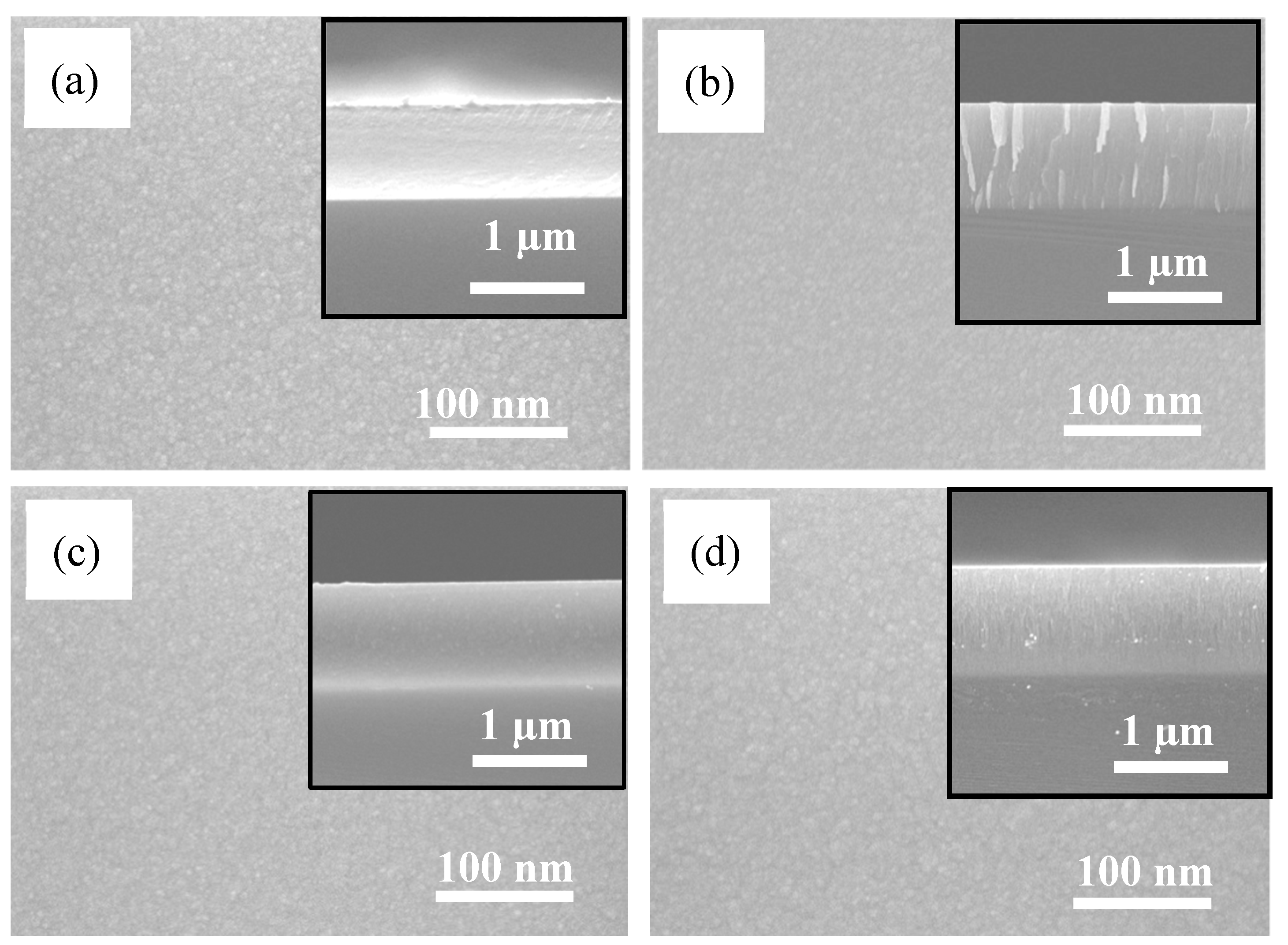
Figure 1. SEM images of Sb-0.14-GaN films sputtered at different heating substrate temperatures: (a) 100 °C, (b) 200 °C, (c) 300 °C and (d) 400 °C.
Coatings 11 00752 g001
Figure 2. 3D AFM of SbGaN films at different sputtering temperatures of (a) 100 °C, (b) 200 °C, (c) 300 °C, and (d) 400 °C.
Coatings 11 00752 g002
Figure 3. XRD patterns of SbGaN films deposited at heating substrate temperatures ranging from 100 to 400 °C.
Coatings 11 00752 g003
Figure 4. Electrical properties of Sb0.14GaN films deposited at different substrate temperature ranges of 100–400 °C.
Coatings 11 00752 g004
Figure 5. Plots of (αhν)2 vs. photon energy (hν) for the optical band gap determination of the Sb0.14GaN films sputtered at different substrate temperatures.
Coatings 11 00752 g005
Figure 6. The current density–voltage characteristic of the p-Sb0.14GaN/n-Si heterojunction diode investigated (a) at room temperature and (b) at the different temperature ranges from 25 °C to 150 °C.
Coatings 11 00752 g006
Figure 7. The reverse and forward current density–voltage (I–V) plots of the p-Sb0.14GaN/n-Si heterojunction diodes measured at the different temperatures, ranging from 25 °C to 150 °C.
Coatings 11 00752 g007
Figure 8. Plots of dV/dln(I) versus current density for p-Sb0.14GaN/n-Si diodes measured at the different temperature.
Coatings 11 00752 g008
Table 1. The Composition of EDS Analyzing Data of the Deposited Sb0.14GaN Films at Heating Substrate Temperatures of 100, 200, 300, and 400 °C.
Temperature Deposition (°C)Ga (at. %)Sb (at. %)N (at. %)[Sb] /([Ga]+[Sb])[N] /([Ga]+[Sb])
10046.483.2450.280.0651.011
20046.313.9149.780.0780.991
30045.894.9249.190.0970.968
40045.645.2349.130.1030.966
Table 2. The effects of Sputtering Temperature on the Structural Properties of Sb0.14GaN Film.
Temperature Deposition (°C)Film Thickness
(µm)
Deposition Rate
(nm/min)
Roughness
(nm)
1001.0033.331.55
2001.1337.671.45
3001.1739.001.26
4001.2441.331.66
Table 3. Structural Properties of Sb0.14GaN Thin Films Deposited at Temperatures Ranging from 100 to 400 °C from the X-ray Diffraction Analyses.
Temperature Deposition (°C)
( 10 1 ¯ 0 )   Peak
a (Å)c (Å)Volume (Å3) FWHM   ( 10 1 ¯ 0 )
(Degree)
Crystallite
Size (nm)
10032.153.2125.2346.700.3724
20032.153.2125.2346.690.3824
30032.203.215.2246.600.4222
40032.263.205.2146.230.5118
Table 4. The Electrical Properties of Sb0.14GaN Films Deposited at the Different Substrate Temperatures.
Deposition Temperature
(°C)
TypeConcentration Np
cm−3
Mobility µ
cm2V−1s−1
Conductivity σ
Scm−1
100p3.25 × 10143850.020
200p1.44 × 10152890.067
300p2.83 × 10162871.300
400p8.97 × 10161462.100
Table 5. The Parameters and the Electrical Characteristics of the p-Sb0.14GaN/n-Si Diode Tested at Different Temperatures.
SamplesLeakage Current Density (A/cm2) at −5 VBarrier
Height (eV)
I-VCheungs’ dV/dlnI Versus I
nRS (kΩ)n
25 °C5.13 × 10−50.455.607.515.59
75 °C1.26 × 10−40.584.006.723.93
100 °C5.98 × 10−40.564.761.374.78
125 °C1.53 × 10−20.545.310.535.36
150 °C2.96 × 10−20.525.710.385.74
Publisher’s Note: MDPI stays neutral with regard to jurisdictional claims in published maps and institutional affiliations.