
Physical Properties of Fe3Si Films Coated through Facing Targets Sputtering after Microwave Plasma Treatment

 ,
,
Abstract
:
1. Introduction
2. Materials and Methods
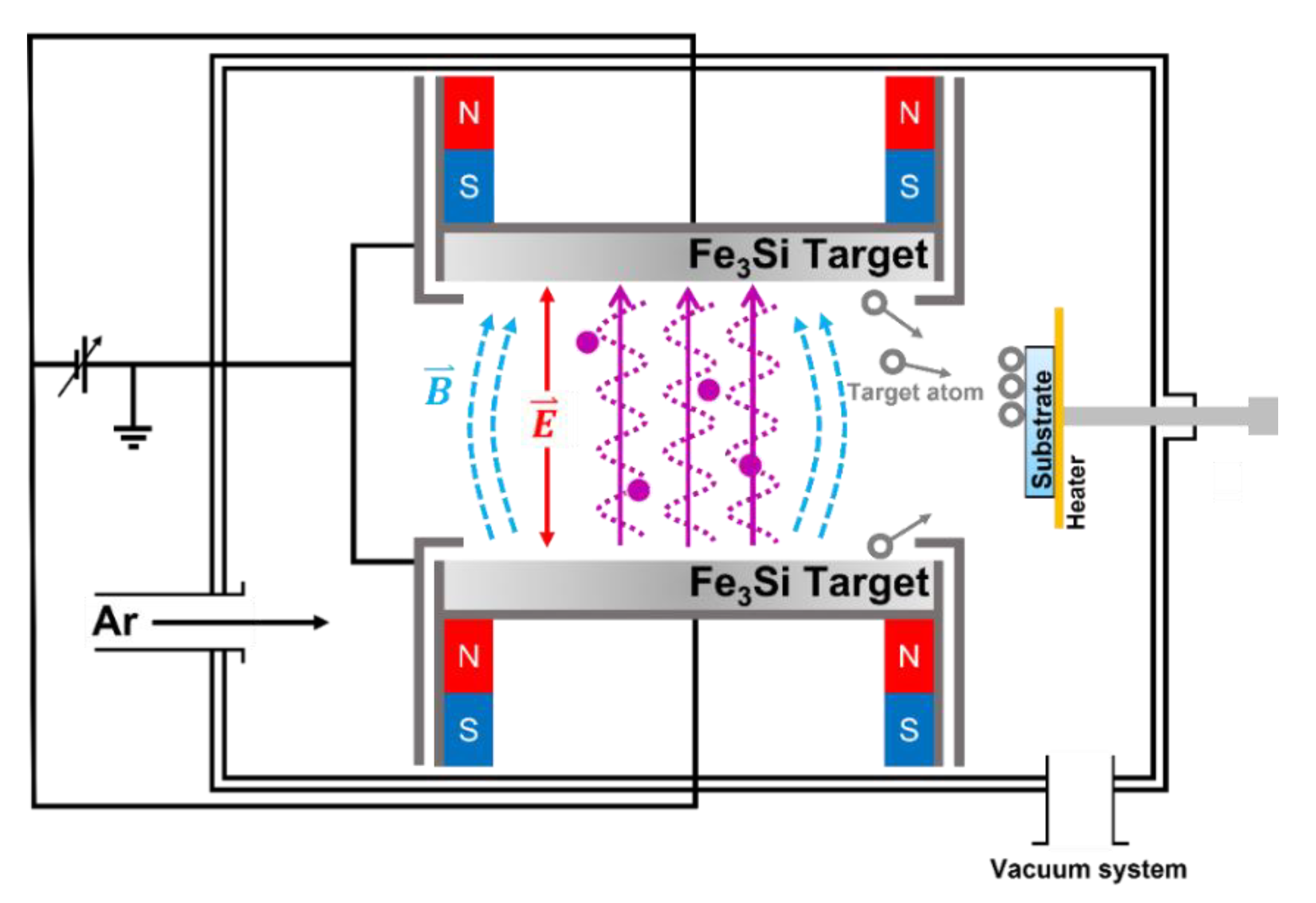
2.1. Epitaxial Creation of Fe3Si Films
2.2. Surface Modification of Fe3Si Films
2.3. Investigation of the Properties of Fe3Si Films
3. Results and Discussion
3.1. Structural Properties of Fe3Si Films
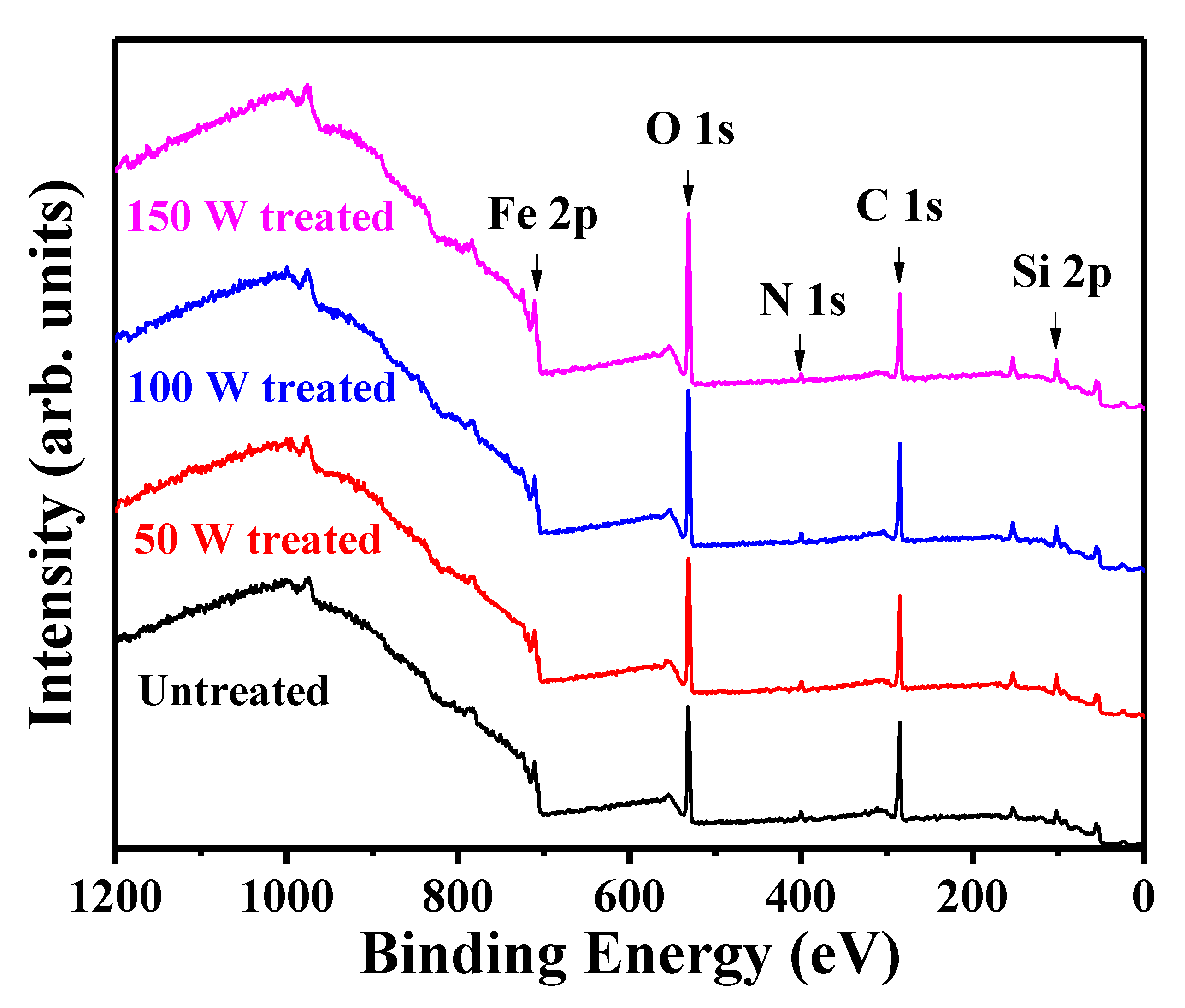
3.2. Chemical Properties of Fe3Si Films
3.3. Surface Morphologies of Fe3Si Films
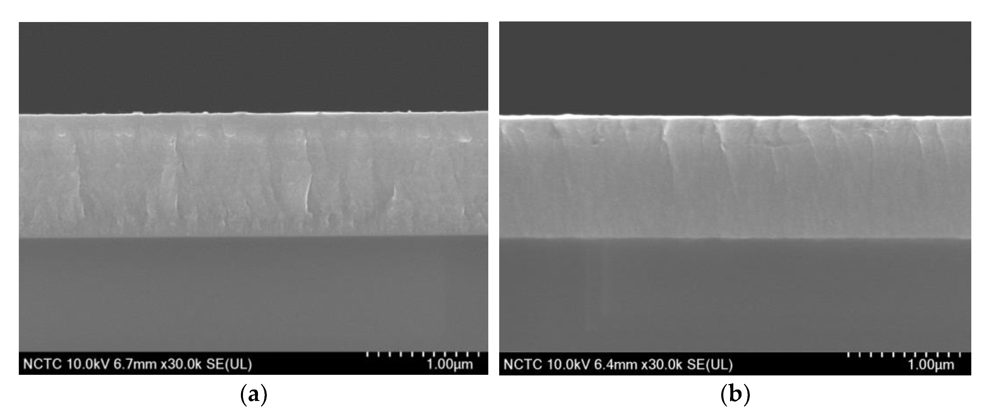
3.3.1. FESEM Images
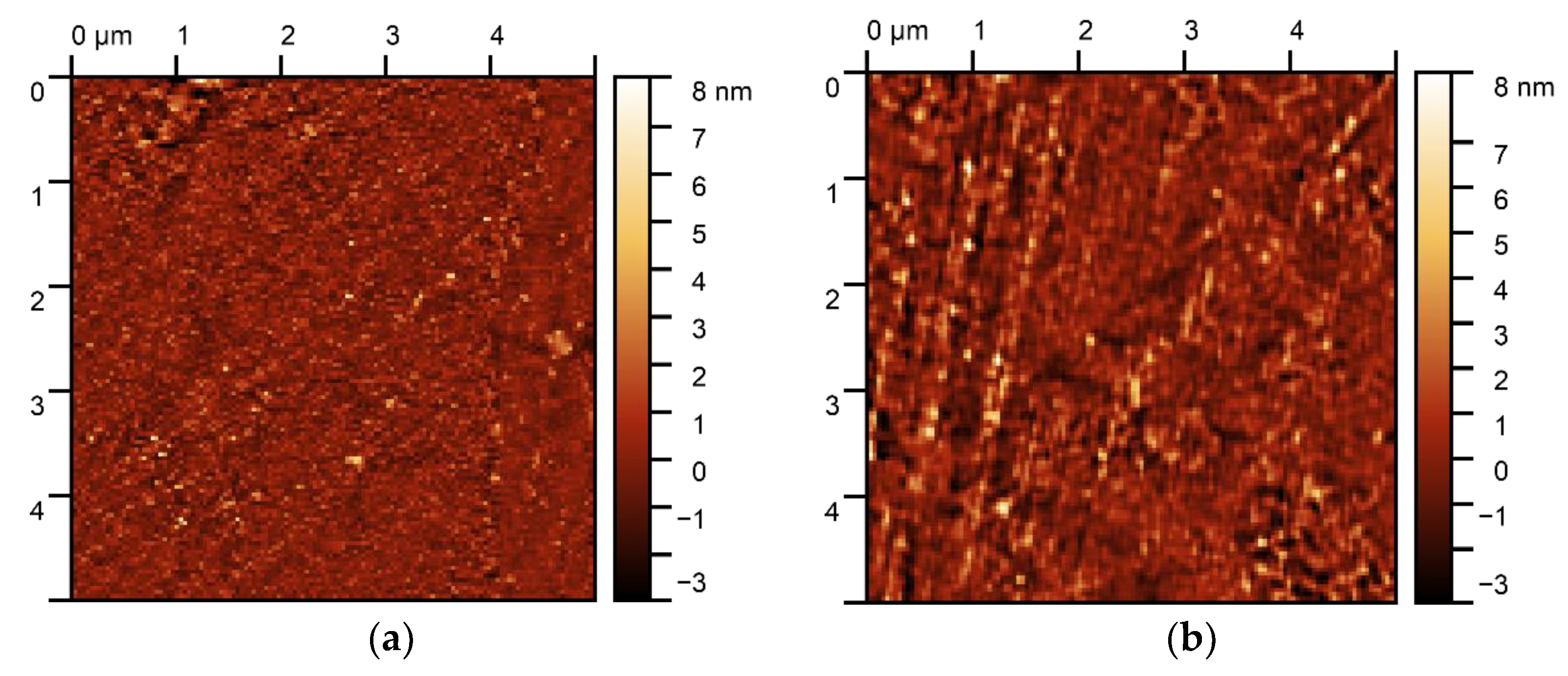
3.3.2. AFM Images
3.4. Wetting Properties of Fe3Si Films
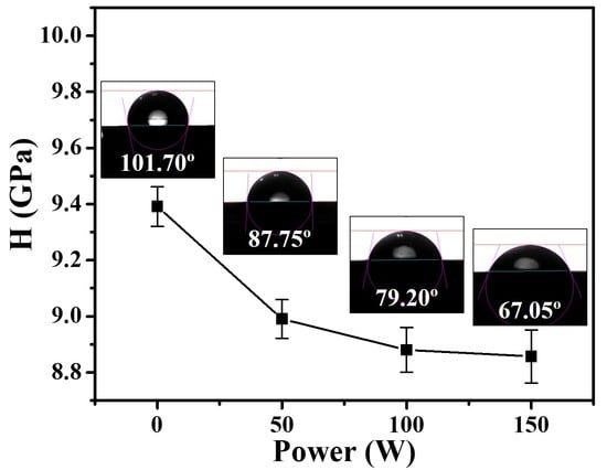
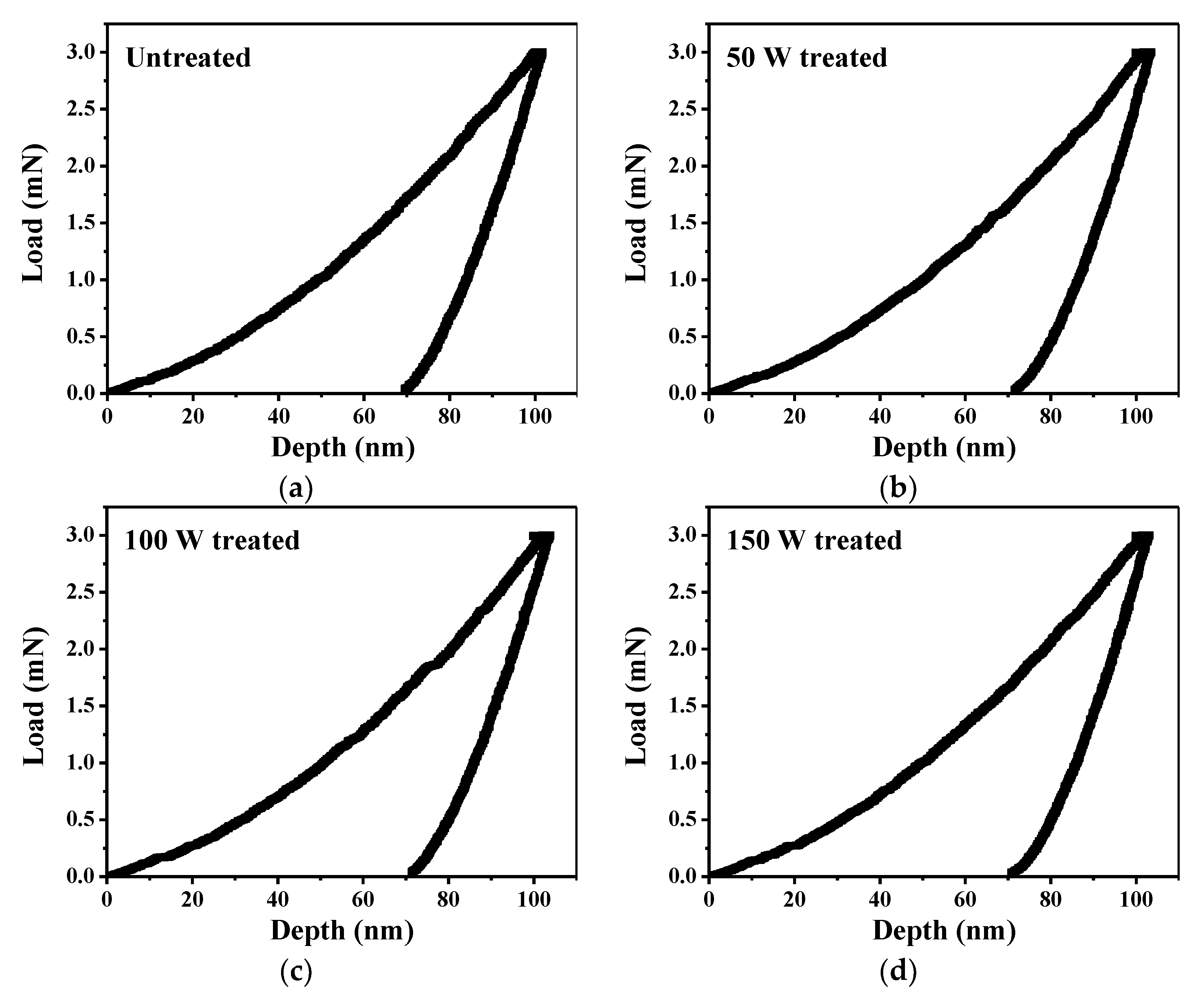
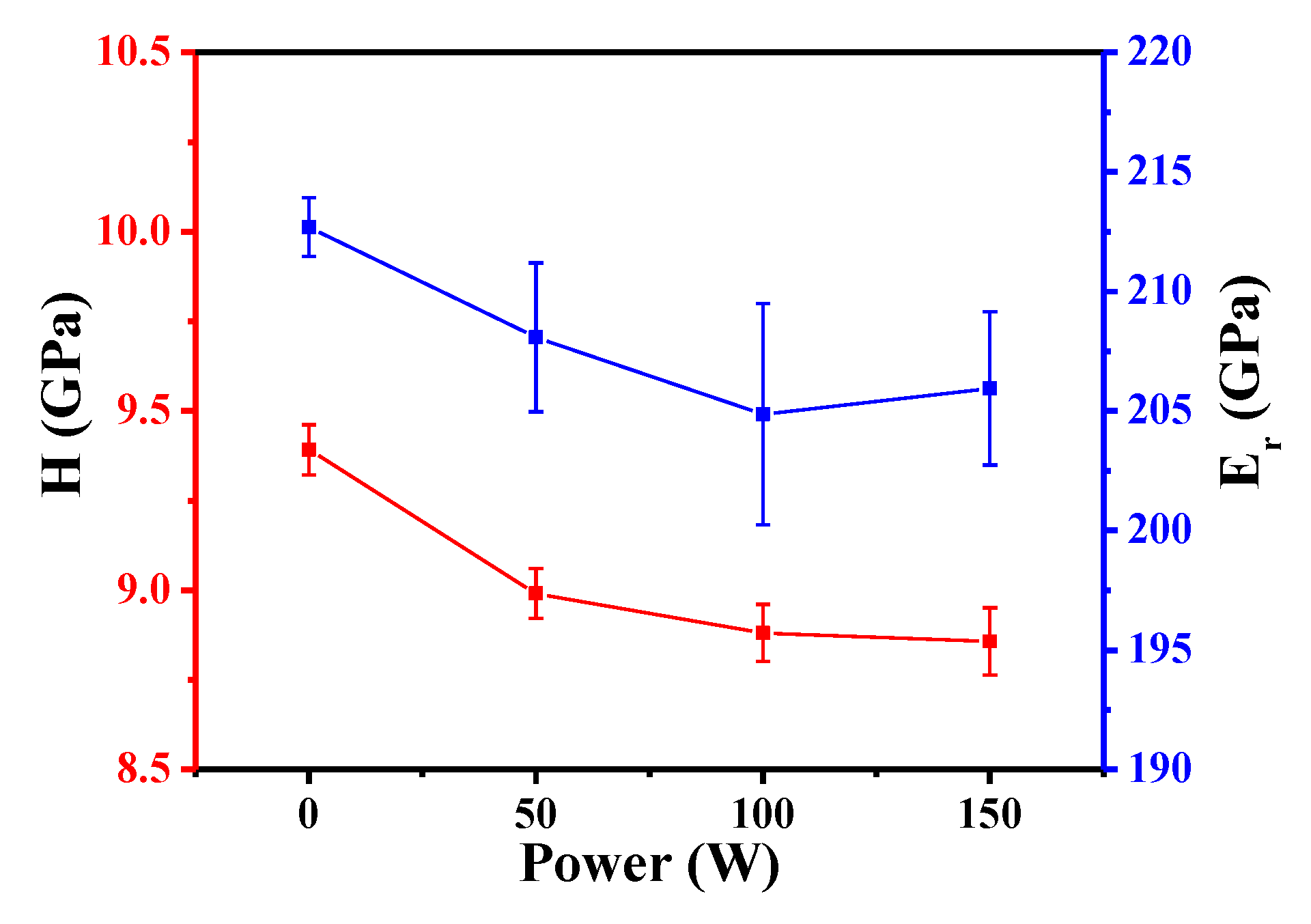
3.5. Mechanical Properties of Fe3Si Films
4. Conclusions
Author Contributions
Funding
Institutional Review Board Statement
Informed Consent Statement
Data Availability Statement
Acknowledgments
Conflicts of Interest
References
- Tam, P.L.; Cao, Y.; Nyborg, L. XRD and XPS characterisation of transition metal silicide thin films. Surf. Sci. 2012, 606, 329–336. [Google Scholar] [CrossRef]
- Promros, N.; Yamashita, K.; Iwasaki, R.; Yoshitake, T. Effects of hydrogen passivation on near-infrared photodetection of n-type β-FeSi2/p-type Si heterojunction photodiodes. Jpn. J. Appl. Phys. 2012, 51, 108006. [Google Scholar] [CrossRef]
- Shaban, M.; Nakashima, K.; Yokoyama, W.; Yoshitake, T. Photovoltaic properties of n-type β-FeSi2/p-type Si heterojunctions. Jpn. J. Appl. Phys. 2007, 46, L667. [Google Scholar] [CrossRef]
- Nakagauchi, D.; Yoshitake, T.; Nagayama, K. Fabrication of ferromagnetic Fe3Si thin films by pulsed laser deposition using an Fe3Si target. Vacuum 2004, 74, 653–657. [Google Scholar] [CrossRef]
- Yoshitake, T.; Nakagauchi, D.; Ogawa, T.; Itakura, M.; Kuwano, N.; Tomokiyo, Y.; Kajiwara, T.; Nagayama, K. Room-Temperature epitaxial growth of ferromagnetic Fe3Si films on Si(111) by facing target direct-current sputtering. Appl. Phys. Lett. 2005, 86, 262505. [Google Scholar] [CrossRef]
- Sittimart, P.; Duangrawa, A.; Onsee, P.; Teakchaicum, S.; Nopparuchikun, A.; Promros, N. Interface state density and series resistance of n-type nanocrystalline FeSi2/p-Type Si heterojunctions formed by utilizing facing-target direct-current sputtering. J. Nanosci. Nanotechnol. 2018, 18, 1841–1846. [Google Scholar] [CrossRef]
- Charoenyuenyao, P.; Promros, N.; Chaleawpong, R.; Saekow, B.; Porntheeraphat, S.; Yoshitake, T. Effect of annealing on surface morphology and wettability of NC-FeSi2 films produced via facing-target direct-current sputtering. J. Nanosci. Nanotechnol. 2019, 19, 6834–6840. [Google Scholar] [CrossRef]
- Mazurenko, V.V.; Shorikov, A.O.; Lukoyanov, A.V.; Kharlov, K.; Gorelov, E.; Lichtenstein, A.I.; Anisimov, V.I. Metal-insulator transitions and magnetism in correlated band insulators: FeSi and Fe1−xCoxSi. Phys. Rev. B 2010, 81, 125131. [Google Scholar] [CrossRef] [Green Version]
- Sadoh, T.; Takeuchi, H.; Ueda, K.; Kenjo, A.; Miyao, M. Epitaxial growth of ferromagnetic silicide Fe3Si on Si(111) substrate. Jpn. J. Appl. Phys. 2006, 45, 3598. [Google Scholar] [CrossRef]
- Hamaya, K.; Ueda, K.; Kishi, Y.; Ando, Y.; Sadoh, T.; Miyao, M. Epitaxial ferromagnetic Fe3Si/Si(111) structures with high-quality heterointerfaces. Appl. Phys. Lett. 2008, 93, 132117. [Google Scholar] [CrossRef] [Green Version]
- Herfort, J.; Schönherr, H.P.; Ploog, K.H. Epitaxial growth of Fe3Si/GaAs(001) hybrid structures. Appl. Phys. Lett. 2003, 83, 3912–3914. [Google Scholar] [CrossRef]
- Lin, F.; Jiang, D.; Ma, X.; Shi, W. Structural order and magnetic properties of Fe3Si/Si(100) heterostructures grown by pulsed-laser deposition. Thin Solid Films 2007, 515, 5353–5356. [Google Scholar] [CrossRef]
- Schneeweiss, O.; Pizurova, N.; Jiraskova, Y.; Žák, T.; Cornut, B. Fe3Si Surface coating on SiFe Steel. J. Magn. Magn. Mater. 2000, 215, 115–117. [Google Scholar] [CrossRef]
- Hirakawa, S.I.; Sonoda, T.; Sakai, K.I.; Takeda, K.; Yoshitake, T. Temperature-dependent current-induced magnetization switching in Fe3Si/FeSi2/Fe3Si trilayered films. Jpn. J. Appl. Phys. 2011, 50, 08JD06. [Google Scholar] [CrossRef]
- Takeda, K.; Yoshitake, T.; Nakagauchi, D.; Ogawa, T.; Hara, D.; Itakura, M.; Kuwano, N.; Tomokiyo, Y.; Kajiwara, T.; Nagayama, K. Epitaxy in Fe3Si/FeSi2 superlattices prepared by facing target direct-current sputtering at room temperture. Jpn. J. Appl. Phys. 2007, 46, 7846. [Google Scholar] [CrossRef]
- Sakai, K.I.; Noda, Y.; Daio, T.; Tsumagari, D.; Tominaga, A.; Takeda, K.; Yoshitake, T. Current-induced magnetization switching at low current densities in current-perpendicular-to-plane structural Fe3Si/FeSi2 artificial lattices. Jpn. J. Appl. Phys. 2014, 53, 02BC15. [Google Scholar] [CrossRef]
- Pransilp, P.; Kiatkamjornwong, S.; Bhanthumnavin, W.; Paosawatyanyong, B. Plasma Nano-modification of poly (ethylene terephthalate) fabric for pigment adhesion enhancement. J. Nanosci. Nanotechnol. 2012, 12, 481–488. [Google Scholar] [CrossRef]
- Taweesub, K.; Visuttipitukul, P.; Tungkasmita, S.; Paosawatyanyong, B. Nitridation of Al–6%Cu alloy by rf plasma process. Surf. Coat. Technol. 2010, 204, 3091–3095. [Google Scholar] [CrossRef]
- Berman, D.; Krim, J. Impact of oxygen and argon plasma exposure on the roughness of gold film surfaces. Thin Solid Films 2012, 520, 6201–6206. [Google Scholar] [CrossRef]
- Surdu-Bob, C.C.; Sullivan, J.L.; Saied, S.O.; Layberry, R.; Aflori, M. Surface compositional changes in gaas subjected to argon plasma treatment. Appl. Surf. Sci. 2012, 202, 183–198. [Google Scholar] [CrossRef]
- Prysiazhnyi, V.; Slavicek, P.; Mikmekova, E.; Klima, M. Influence of chemical precleaning on the plasma treatment efficiency of aluminum by rf plasma pencil. Plasma Sci. Technol. 2016, 18, 430–437. [Google Scholar] [CrossRef]
- Ujino, D.; Nishizaki, H.; Higuchi, S.; Komasa, S.; Okazaki, J. Effect of plasma treatment of titanium surface on biocompatibility. Appl. Sci. 2019, 9, 2257. [Google Scholar] [CrossRef] [Green Version]
- Ruand, L.; Jie-Rong, C. Studies on wettability of medical Poly (Vinyl Chloride) by remote argon plasma. Appl. Surf. Sci. 2006, 252, 5076–5082. [Google Scholar]
- Lin, C.; Sun, D.C.; Ming, S.L.; Jiang, E.Y.; Liu, Y.G. Magnetron facing target sputtering system for fabricating single-crystal films. Thin Solid Films 1996, 279, 49–52. [Google Scholar] [CrossRef]
- Odrobina, I.; Kúdela, J.; Kando, M. Characteristics of the planar plasma source sustained by microwave power. Plasma Sources Sci. Technol. 1998, 7, 238. [Google Scholar] [CrossRef]
- Tang, C.B.; Wen, F.R.; Chen, H.X.; Liu, J.J.; Tao, G.Y.; Xu, N.J.; Xue, J.Q. Corrosion characteristics of Fe3Si intermetallic coatings prepared by molten salt infiltration in sulfuric acid solution. J. Alloys Compd. 2019, 778, 972–981. [Google Scholar] [CrossRef]
- Chang-Bin, T.; Hong-Xia, C.; Fu-Rong, W.; Ni-Jun, X.; Wei, H.; Juan-Qin, X. Facile preparation and tribological property of alloyed Fe3Si coatings on stainless steels surface by molten-salt infiltration method. Surf. Coat. Technol. 2020, 397, 126049. [Google Scholar] [CrossRef]
- Sattar, H.; Jielin, S.; Ran, H.; Imran, M.; Ding, W.; Gupta, P.D.; Ding, H. Impact of microstructural properties on hardness of tungsten heavy alloy evaluated by stand-off LIBS after PSI plasma irradiation. J. Nucl. Mater. 2020, 540, 152389. [Google Scholar] [CrossRef]
- Lin, W.T.; Chen, S.H.; Chan, S.H.; Hu, S.C.; Peng, W.X.; Lu, Y.T. Crystallization phase transition in the precursors of CIGS films by Ar-ion plasma etching process. Vacuum 2014, 99, 1–6. [Google Scholar] [CrossRef]
- Fernández, S.; Santos, J.D.; Munuera, C.; García-Hernández, M.; Naranjo, F.B. Effect of Argon Plasma-treated polyethylene terepthalate on ZnO:Al properties for flexible thin film silicon solar cells applications. Sol. Energy Mater. Sol. Cells 2015, 133, 170–179. [Google Scholar] [CrossRef]
- Madera, R.G.B.; Martinez, M.M.; Vasquez, M.R. Effects of rf plasma treatment on spray-pyrolyzed copper oxide films on silicon substrates. Jpn. J. Appl. Phys. 2017, 57, 01AB05. [Google Scholar] [CrossRef]
- Douglas, E.A.; Sheng, J.J.; Verley, J.C.; Carroll, M.S. Argon-Germane In Situ Plasma Clean for Reduced Temperature Ge on Si Epitaxy by High Density Plasma Chemical Vapor Deposition. J. Vac. Sci. Technol. 2015, 33, 41202. [Google Scholar] [CrossRef]
- Chen, G.L.; Peng, J.H.; Xu, W.X. Surface reaction of polycrystalline Fe3Si alloys with oxygen and water vapor. Intermetallics 1998, 6, 315–322. [Google Scholar] [CrossRef]
- Calaway, M.J.; Fries, M.D. Adventitious Carbon on Primary Sample Containment Metal Surfaces. In Proceedings of the 46th Lunar and Planetary Science Conference, The Woodlands Waterway Marriott Hotel and Convention Center, The Woodlands, TX, USA, 16–20 March 2015; p. 1517. [Google Scholar]
- Yoshitake, T.; Inokuchi, Y.; Yuri, A.; Nagayama, K. Direct epitaxial growth of semiconducting β-FeSi2 thin films on Si(111) by facing targets direct-current sputtering. Appl. Phys. Lett. 2006, 88, 182104. [Google Scholar] [CrossRef]
- Shaban, M.; Nomoto, K.; Izumi, S.; Yoshitake, T. n-type β-FeSi2/intrinsic-si/p-type si heterojunction photodiodes for near-infrared light detection at room temperature. Appl. Phys. Lett. 2009, 94, 222113. [Google Scholar] [CrossRef]
- Promros, N.; Baba, R.; Takahara, M.; Mostafa, T.M.; Sittimart, P.; Shaban, M.; Yoshitake, T. Epitaxial growth of β-FeSi2 thin films on Si(111) substrates by radio frequency magnetron sputtering and their application to near-infrared photodetection. Jpn. J. Appl. Phys. 2016, 55, 06HC03. [Google Scholar] [CrossRef]
- Abd Jelil, R. A Review of low-temperature plasma treatment of textile materials. J. Mater. Sci. 2015, 50, 5913–5943. [Google Scholar] [CrossRef]
- He, L.P.; Cai, Z.B.; Peng, J.F.; Deng, W.L.; Li, Y.; Yang, L.Y.; Zhu, M.H. Effects of oxidation layer and roughness on the fretting wear behavior of copper under electrical contact. Mater. Res. Express 2020, 6, 1265e3. [Google Scholar] [CrossRef]
- Junior, C.F.L.; de Assis Machado, G.S.; Mendes, P.S.N.; Huguenin, J.A.O.; Ferreira, E.A.; da Silva, L. Analysis of copper and zinc alloy surface by exposure to alcohol aqueous solutions and sugarcane liquor. J. Mater. Res. Technol. 2020, 9, 2545–2556. [Google Scholar] [CrossRef]
- Lavieja, C.; Oriol, L.; Peña, J.I. Creation of superhydrophobic and superhydrophilic surfaces on ABS employing a nanosecond laser. Materials 2018, 11, 2547. [Google Scholar] [CrossRef] [Green Version]
- Charoenyuenyao, P.; Promros, N.; Chaleawpong, R.; Borwornpornmetee, N.; Sittisart, P.; Tanaka, Y.; Yoshitake, T. Impact of annealing temperature and carbon doping on the wetting and surface morphology of semiconducting iron disilicide formed via radio frequency magnetron sputtering. Thin Solid Films 2020, 709, 138248. [Google Scholar] [CrossRef]
- Quéré, D. wetting and roughness. Annu. Rev. Mater. Res. 2018, 38, 71–99. [Google Scholar] [CrossRef]
- Wenzel, R.N. surface roughness and contact angle. J. Phys. Chem. 1949, 53, 1466–1467. [Google Scholar] [CrossRef]
- Cassie, A.B.D.; Baxter, S. Wettability of porous surfaces. J. Chem. Soc. Faraday Trans. 1944, 40, 546–551. [Google Scholar] [CrossRef]
- Fischer-Cripps, A.C. A review of analysis methods for sub-micron indentation testing. Vacuum 2000, 58, 569–585. [Google Scholar] [CrossRef]
- Lu, C.J.; Bogy, D.B. The Effect of tip radius on nano-indentation hardness tests. Int. J. Solids Struct. 1995, 32, 1759–1770. [Google Scholar] [CrossRef]
- Oliver, W.C.; Pharr, G.M. An improved technique for determining hardness and elastic modulus using load and displacement sensing indentation experiments. J. Mater. Res. 1992, 7, 1564–1583. [Google Scholar] [CrossRef]
- Beegan, D.; Chowdhury, S.; Laugier, M.T. Comparison between nanoindentation and scratch test hardness (scratch hardness) values of copper thin films on oxidised silicon substrates. Surf. Coat. Technol. 2007, 201, 5804–5808. [Google Scholar] [CrossRef]
- Murakami, T.; Hibi, Y.; Mano, H.; Matsuzaki, K.; Inui, H. Friction and wear properties of fe-si intermetallic compounds in ethyl alcohol. Intermetallics 2012, 20, 68–75. [Google Scholar] [CrossRef]
- Chen, L.; Ahadi, A.; Zhou, J.; Ståhl, J.-E. Modeling effect of surface roughness on nanoindentation tests. Procedia CIRP 2013, 8, 334–339. [Google Scholar] [CrossRef] [Green Version]


| Sample | Surface Atomic Concentration (at.%) | ||||
|---|---|---|---|---|---|
| Fe 2p | O 1s | N 1s | C 1s | Si 2p | |
| Untreated | 10.30 | 47.19 | 3.28 | 35.68 | 3.55 |
| Ar treated (50 W; 10 min) | 12.78 | 53.07 | 2.87 | 26.47 | 4.81 |
| Ar treated (100 W; 10 min) | 13.61 | 56.15 | 2.00 | 23.48 | 4.76 |
| Ar treated (150 W; 10 min) | 15.49 | 56.23 | 2.02 | 20.35 | 5.92 |
| Sample | H (GPa) | Er (GPa) |
|---|---|---|
| Untreated | 9.392 ± 0.070 | 204.862 ± 1.226 |
| Ar treated (50 W; 10 min) | 8.991 ± 0.069 | 205.943 ± 4.633 |
| Ar treated (100 W; 10 min) | 8.881 ± 0.080 | 208.085 ± 3.113 |
| Ar treated (150 W; 10 min) | 8.857 ± 0.094 | 212.693 ± 3.211 |
Publisher’s Note: MDPI stays neutral with regard to jurisdictional claims in published maps and institutional affiliations. |
© 2021 by the authors. Licensee MDPI, Basel, Switzerland. This article is an open access article distributed under the terms and conditions of the Creative Commons Attribution (CC BY) license (https://creativecommons.org/licenses/by/4.0/).
Share and Cite
Borwornpornmetee, N.; Charoenyuenyao, P.; Chaleawpong, R.; Paosawatyanyong, B.; Phatthanakun, R.; Sittimart, P.; Aramaki, K.; Hamasaki, T.; Yoshitake, T.; Promros, N. Physical Properties of Fe3Si Films Coated through Facing Targets Sputtering after Microwave Plasma Treatment. Coatings 2021, 11, 923. https://doi.org/10.3390/coatings11080923
Borwornpornmetee N, Charoenyuenyao P, Chaleawpong R, Paosawatyanyong B, Phatthanakun R, Sittimart P, Aramaki K, Hamasaki T, Yoshitake T, Promros N. Physical Properties of Fe3Si Films Coated through Facing Targets Sputtering after Microwave Plasma Treatment. Coatings. 2021; 11(8):923. https://doi.org/10.3390/coatings11080923
Chicago/Turabian StyleBorwornpornmetee, Nattakorn, Peerasil Charoenyuenyao, Rawiwan Chaleawpong, Boonchoat Paosawatyanyong, Rungrueang Phatthanakun, Phongsaphak Sittimart, Kazuki Aramaki, Takeru Hamasaki, Tsuyoshi Yoshitake, and Nathaporn Promros. 2021. "Physical Properties of Fe3Si Films Coated through Facing Targets Sputtering after Microwave Plasma Treatment" Coatings 11, no. 8: 923. https://doi.org/10.3390/coatings11080923
APA StyleBorwornpornmetee, N., Charoenyuenyao, P., Chaleawpong, R., Paosawatyanyong, B., Phatthanakun, R., Sittimart, P., Aramaki, K., Hamasaki, T., Yoshitake, T., & Promros, N. (2021). Physical Properties of Fe3Si Films Coated through Facing Targets Sputtering after Microwave Plasma Treatment. Coatings, 11(8), 923. https://doi.org/10.3390/coatings11080923