Abstract
We unveiled the effect of doping on the morpho-structural and opto/electrical properties of Ca-doped ZnO:Al thin films obtained by RF magnetron sputtering. Scanning electron microscopy (SEM) was performed to reveal the surface morphology, while the composition and crystal structure were investigated by energy dispersive X-ray spectroscopy (EDX) and X-ray diffraction (XRD). The correlation between the microstructure and the electrical conductivity identifies an increase in electrical conductivity up to 145 × 10−3 Ω−1·m−1 at 5 wt.% Ca doping level with the decrease in the grain size. Furthermore, the presence of Ca dopant triggers the occurrence of the emission peak at 430 nm and an increase of the green emission peak in PL spectra. Corroborating the electrical measurements with X-ray diffraction and optical measurements, one can infer that the electrical conductivity is dominated by intrinsic defects developed during deposition and by the existence of dopants.
1. Introduction
Zinc oxide (ZnO) thin films prepared by physical methods such as radio frequency magnetron sputtering continue to be of high interest due to their low cost and low absorption of visible light, triggering an enhanced UV photoresponse of the photodetector, transparent conductive electrodes in solar cells, and fluorescence imaging performance [1,2,3].
In addition to good absorptivity, high conductivity is the prerequisite for their applications in electro-optic devices. An effective method to achieve these properties is doping with metals, especially elements of group III (Al, Ga), which have been shown to substitute Zn or O in the ZnO structure to enable n-type doping [4,5,6,7,8,9,10]. Employing a physical deposition approach, Sun et al. [11] studied (Al, Co)–ZnO films cosputtered on glass substrate to reveal that (Co, Al) doping affects the carrier mobility due to the reduce crystallinity in the deposited films. Wang et al. [12] investigated Al and F co-doped zinc oxide (AFZO) thin films on glass substrates by radio frequency magnetron sputtering, when the co-doping induces a significant decrease of the film resistivity in comparison with either Al or F doping, revealing the effectiveness of Al and F co-doping on electrical properties of ZnO thin films.
Besides these intensively investigated ZnO-based alloys, II–VI compounds with a rock salt structure and a band-gap above 7 eV (7.2 eV in the case of calcium oxide and 7.8 in the case of MgO) are known for enhancing the transmittance of the ZnO film [13]. Doped/co-doped ZnO films proved to be suitable materials for both gas sensing and as the constituent of a layered transparent conductive oxide electrode for organic electronics. An efficient transparent conductive gas diffusion barrier, with improved optical, electrical, and moisture/oxygen barrier properties, was developed when periodical dopant layers (Mg- and Al-) were inserted in the ZnO film [14].
Thus, codoping with Al and Ca is an effective way to widen the application field of ZnO-based transparent conductive oxides (TCO) materials [15]. From this perspective, several studies on ZnO:(Ca, Al) co-doped films prepared by sol-gel methods, have shown their potential as sensitive material for CO2 sensors [16], whereas discrete photoluminescence (PL) emission certified the great potential for optical devices applications [17].
Therefore, exploring the physical nature behind, it may provide some effective strategies for optimizing optical and electrical performance of ZnO-based TCO material. Studies on ZnO thin film prepared by atomic layer deposition [18], sol-gel [19], spray pyrolysis [20], chemical vapor deposition [21] and sputtering [22] strongly support the relationship between the deposition technique and the quality of the film. Amongst them, sputtering is the most efficient method of producing high quality and low cost ZnO-based thin films. However, the majority of researchers that have developed ZnO thin films by sputtering have used expensive ceramic targets, which are very fragile, causing cracking problems when raising the temperature. While RF magnetron sputtering is a technology that can provide optimum coating uniformity, and high deposition rate at large scale [23], 99.9% of the CaO sputtering target is a material that quickly breaks down and returns to powder. To circumvent aforesaid issues, an alternative could be represented by the chemical diffusion which is a relatively simply, low-cost and reproducible process. The chemical diffusion is generally involved in the growth of materials to control the shape of particles [24].
In this paper, we synthesized thin Ca doped ZnO: Al 2 wt.% films with Ca concentrations that varies between 1 wt.%, 3 wt.% and 5 wt.%, to show the doping effect to the morpho-structural and opto/electrical properties of the ZnO: Al thin films synthesized by RF magnetron sputtering.
2. Materials and Methods
2.1. Ca-Doped ZnO:Al Thin Film Synthesis
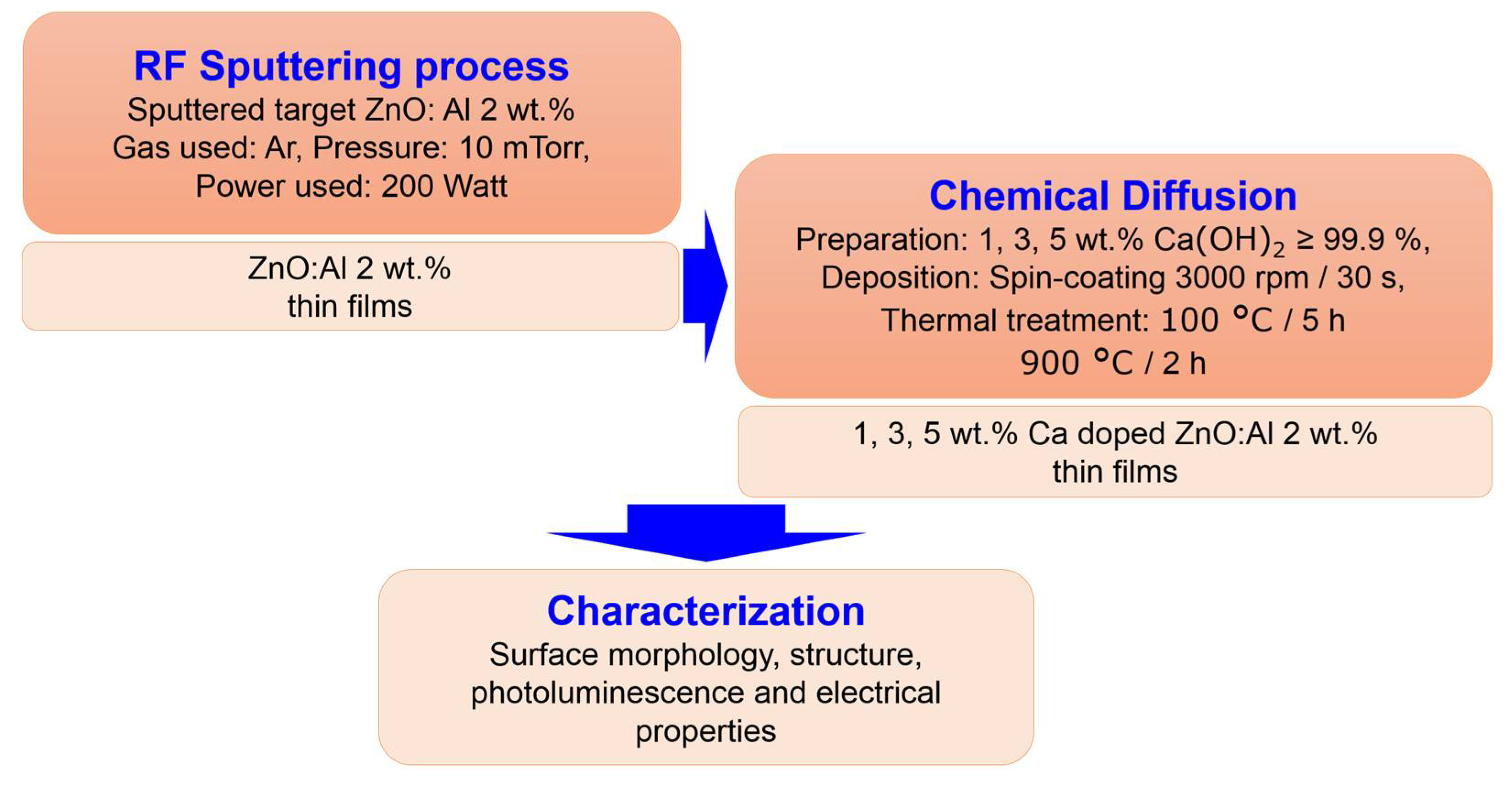
The substrates used for deposition were silicon substrates with (100) crystallographic orientation, 1–10 Ωcm resistivity and 100 nm thermally grown SiO2. Before deposition, the substrates were cleaned in an ultrasound bath with Extran (Merck KGaA, Darmstadt, Germany) and after that in a piranha solution (H2SO4:H2O = 3:1). The flowchart of Ca doped ZnO:Al thin film preparation is presented in Figure 1. Calcium-doped ZnO:Al thin films were prepared in two steps: (1) RF Sputtering process. In order to deposit 2 wt.% Al:ZnO thin films on SiO2/Si substrates, ZnO:Al-2 wt.% target with a 154 mm diameter and 99.99% purity (Tesbourne Ltd.) was used, with a balanced magnetron. In order to deposit stoichiometric films, it is necessary to optimize sufficient amount of oxygen with argon in the sputtering system. Accordingly, the obtained films were deposited with argon (Ar) at a flow rate of 30 sccm and oxygen (O2) at 99.999 purity and 0.5 sccm as sputtering and reactive gases to suppress the oxygen vacancies that act as annihilators of holes during film deposition according to Otieno et al. [25]. The RF power used was 200 W. The depositions were performed with a RF magnetron sputtering PlasmalabSystem400 (Oxford Instruments, Abingdon, UK). The thickness of the 2 wt.% Al:ZnO thin films was 130 nm. (2) Chemical Diffusion. Calcium hydroxide, (99.995% trace metals basis, Sigma-Aldrich, Saint Louis, MO, USA) used as the Ca source, was ultrasonicated in deionized water for 2 h at 40 °C in order to achieve different concentrations of calcium in the solution: 1, 3 and 5 wt.%. The obtained solutions were deposited in a single layer at 3000 rpm/30 s on the ZnO:Al 2% thin films followed by a first thermal treatment at 100 °C = 5 h in order to obtain a partial dehydration and a second thermal treatment at 900 °C = 2 h in air for decomposition of Ca(OH)2.
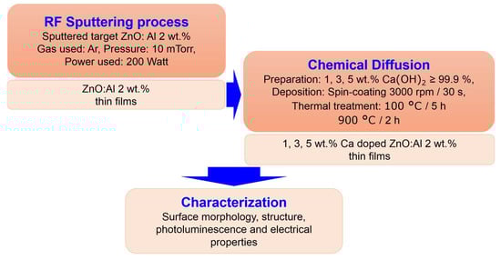
Figure 1.
Flowchart of Ca-doped ZnO:Al 2% thin film preparation.
2.2. Characterization of the Thin Films
The films’ morphology and the thickness were explored by Nova NanoSEM 630 Scanning Electron Microscope (FEI Company, Hillsboro, OR, USA) employing an ultra-high resolution detector at an acceleration voltage of 10 kV. The recognition of Ca concentration and its assigning within the ZnO:Al 2% films surface were achieved with the element energy dispersive spectroscopy (EDS) system (Smart Insight AMETEK, Mahwah, NJ),USA. The energy dispersive X-ray spectroscopy (EDX) was acquired at an acceleration voltage of 10 kV, with a working distance of 5 mm and 30k × magnification. XRD analyses were performed on a Rigaku SmartLab X Ray Diffractometer (Rigaku Corporation, Tokyo, Japan) using CuKα radiation (λ = 1.5406 Å) in grazing incident (GI-XRD) mode with an incident angle of 0.5°. A sampling step of 0.01° and a speed of 4°/min were used. The phase recognition was made using the International Center for Diffraction Data (ICDD) database. The photoluminescence (PL) emission spectra of the films were recorded with an Edinburgh FL920 fluorimeter, at 300 nm excitation wavelength. An EP6/Suss MicroTec microprober and a 4200-SCS/C/Keithley system (Keithley Instruments, Cleveland, OH, USA; Suss MicroTec, Garching bei München, Germany) were used to measure the electrical characteristics of the films. For this purpose, the bottom electrode was defined using e-beam by deposition of a thin film of 10/100 nm Ti/Pt on the SiO2/Si substrate before the Ca dopedZnO:Al layers. Then, a mask (pad size = 0.64 mm2) was used to deposit the Ti/Au (10/100 nm) upper electrodes using the DC Sputtering system—AUTO 500 (BOC Edwards, West Sussex, UK) on the film surface. The sputtering was carried out in a 3 sccm Ar atmosphere, using a power of 45 W and an ultimate vacuum of 1.26 × 10⁻³ mbar.
3. Results and Discussions
3.1. The Morphology Features and Chemical Composition
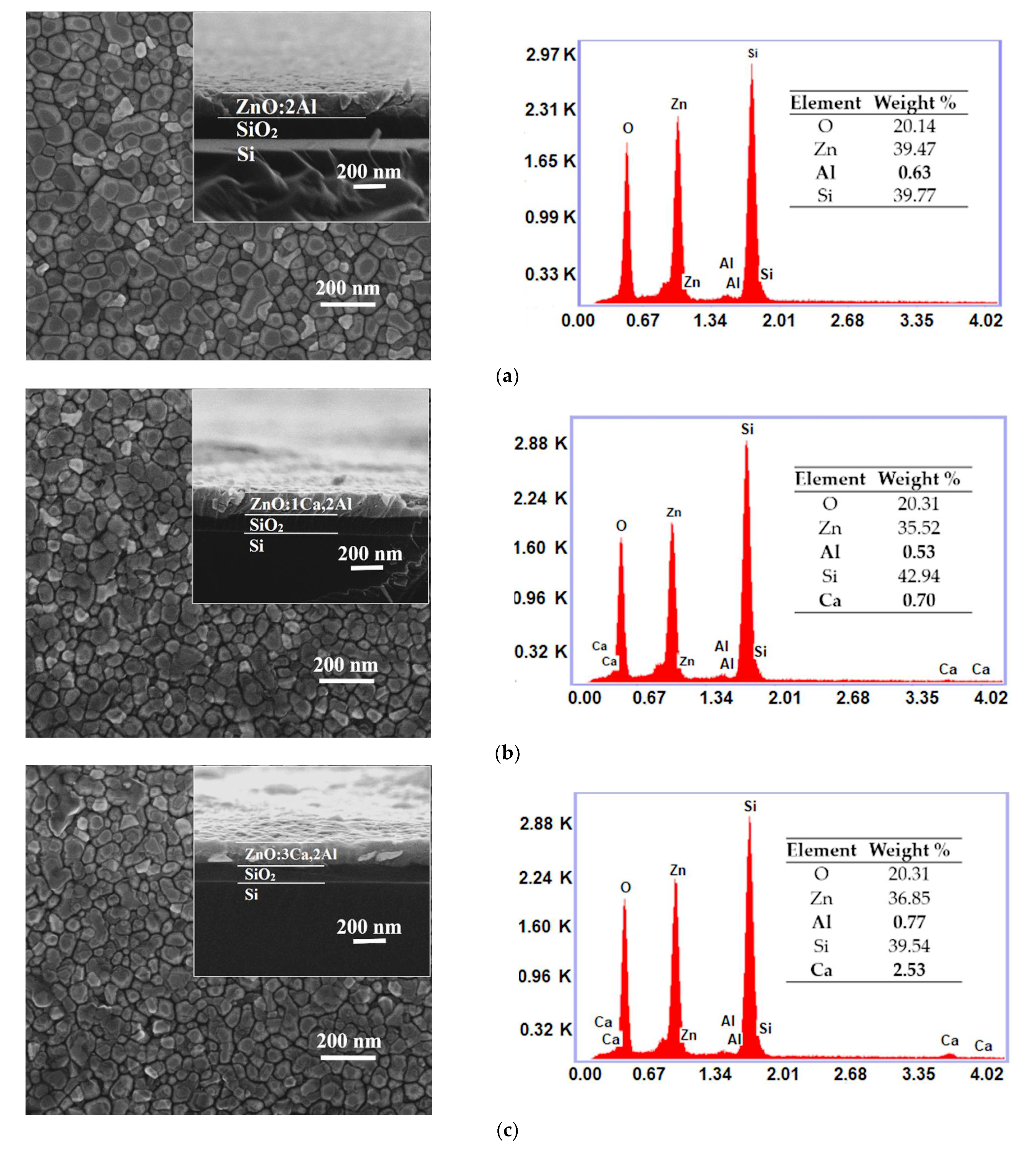
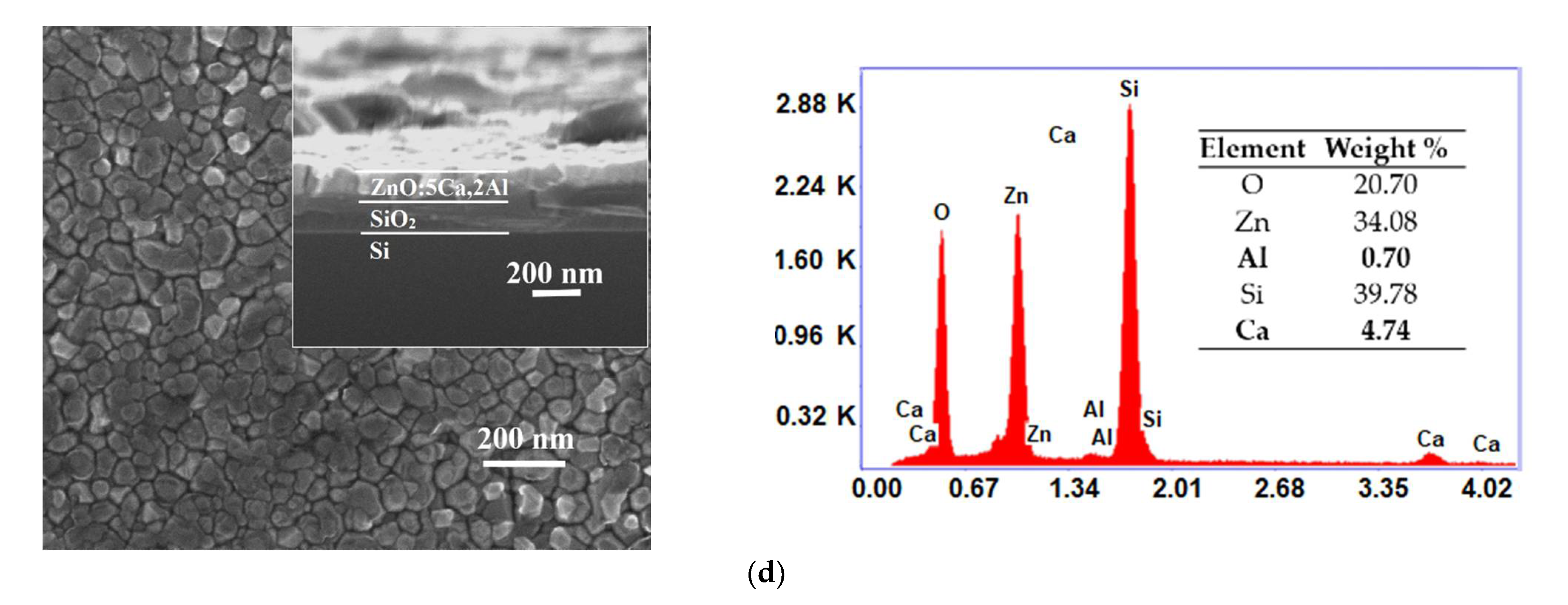
One can observe from top-view SEM micrographs, the surface of the synthesized ZnO:Al films consists from grains uniformly distributed with dimensions raging between 30 and 60 nm. As the Ca content increased, the grain size became smaller, as shown in Figure 2a–d. At the same time, the cross-sectional SEM (inset in Figure 2a–d) indicates that the thickness increased from 130 nm (ZnO:Al 2%) to 160 nm as the doping level reached 5 wt.%. As can be seen, the film shows an obvious vertical columnar microstructure. From the EDX spectra one can identify the presence of Zn, O, Al and Ca, which are the dominant elements in all samples. The determination of the elemental concentration was achieved with EDX analysis of the surface. The weight percentages of these elements for our thin films are presented in the inset table of each EDX spectra.
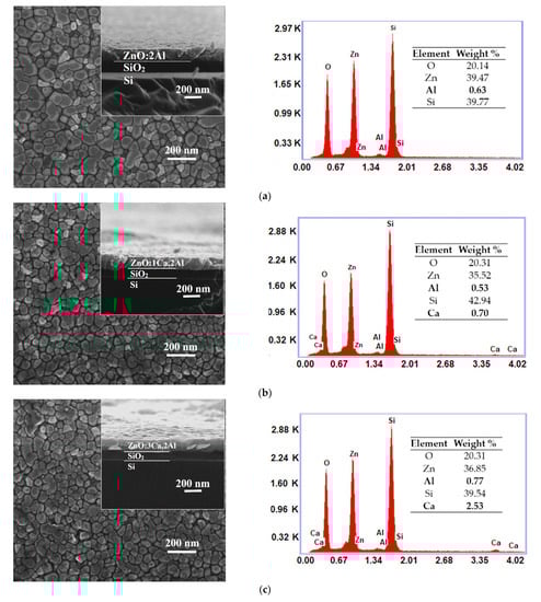
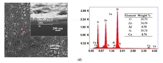
Figure 2.
Surface morphology (inset: cross-sectional image) and EDX spectra of ZnO:Al 2% (a) and Ca-doped ZnO:Al 2% thin films with: 1, 3 and 5% Ca: (b–d).
3.2. Structural Analysis
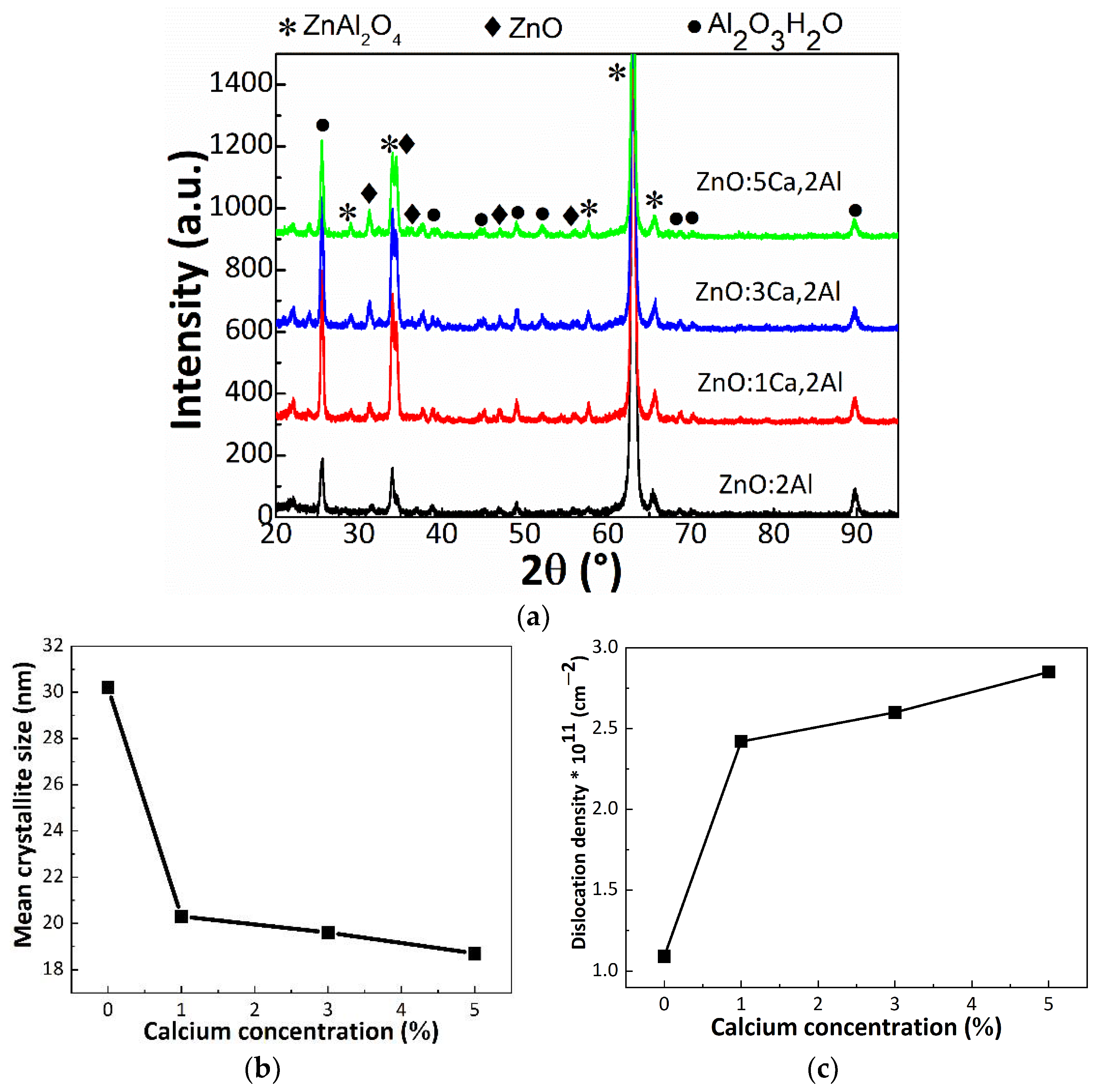
Grazing incidence XRD (GI-XRD) was used to identify the constituent phases. In Figure 3a are presented the GI-XRD patterns recorded for our four samples.
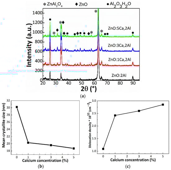
Figure 3.
(a) GI-XRD patterns of ZnO:Al 2% and Ca-doped ZnO:Al 2% thin films with: 1, 3 and 5% Ca, (b) the mean crystallite size and (c) dislocation density of investigated thin films as a function of calcium concentration of the doped ZnO:Al thin films.
Each pattern presents multiple diffraction peaks, further assigned according to the International Crystallography for Diffraction Data (ICDD) database. Accordingly, we identified a phase combination between cubic ZnAl2O4 (gahnite phase), pure wurtzite ZnO and Al2O3H2O (diaspore phase). It could be observed that the calcium incorporation did not lead to additional phases based on calcium oxide. After a careful investigation of the diffraction peaks, one can remark a slight shift to smaller 2θ of ZnO, up to 0.4°. According to the Bragg’s law, a shift of the diffraction peaks to smaller angles reflects an increase of the interplanar distance. Moreover, the shift could be due to the difference in the atomic radius between zinc (1.42 Å) and calcium (1.94 Å), leading to a local distortion of the wurtzite lattice due to some residual stress inside the thin films. In order to attest the crystal quality, the Scherrer equation was used [26]. This gives the correlation between the width of the diffraction peak to the size of the crystalline domains in this way:
where k is a shape factor taken usually equal as 0.9, θ is the peak angular position, λ is the wavelength and β is the full width at half maximum. We found that the mean crystallite sizes decreased from 30.2 nm (ZnO:Al) to 20.1 nm (ZnO:1Ca,2Al) and 19.1 nm (ZnO:3Ca,2Al), reaching 18.7 nm for the last sample with increasing calcium loading varying in the range 30.2–18.7 nm. Meanwhile, the unit cell parameters of ZnO lattice increases. For instance, a increased from 3.24 to 3.28 Å, while c from 5.20 to 5.25 Å. The values of the mean crystallite size for ZnAl2O4 and its lattice constant, as well as the lattice parameters of ZnO are tabulated in Table 1.
τ = kλ/(βcosθ)

Table 1.
Mean crystallite size (nm)—ZnAl2O4, the lattice constant (Å)—ZnAl2O4 and the lattice constant (Å) ZnO.
The unit cell parameters were calculated from the interplanar distances, was calculated using the Bragg’s law, , where is the angular position of the diffraction peak. Further, standard relations for cubic and hexagonal lattice were used to get the unit cell parameters [27]. For cubic crystals, the interplanar distance is related to the unit cell parameter thus:
The and lattice parameters of the hexagonal crystal were calculated thus:
The out-of-plane lattice parameter was determined from the symmetric ( = = 0) reflection, and used further to obtain the in-plane lattice parameter , which is determined from the asymmetric reflection.
It is clear that the doping affects the lattice parameter of ZnO, giving rise to a tensile strain of 1.2% and 0.9% on the a- and c-axis, respectively. At the same time, the lattice constant of cubic ZnAl2O4 remains constant during Ca doping. Moreover, the doping is related to a worse crystal quality, since the mean crystallite size decreased. In this view, the results suggest that the Ca dopant has different effects. One the one hand, in the case of ZnO, where the lattice constant is subjected to an expansion, it seems that the Ca dopant acts as an interstitial defect [28]. Moreover, the crystal quality is not altered at different Ca doping stages. On the other hand, in the case of ZnAl2O4, the dopant has another effect. Although the lattice constant remains unmodified, the mean crystallite size decreases. In this regard, the Ca dopant most probably substituted an atom from ZnAl2O4 host lattice. Further, the dislocation density was estimated as the inverse of the mean crystallite size square: 1/τ2. Accordingly, the dislocation density increases from 1.1 × 1011 cm−2 to 28.2 × 1011 cm−2 for 5% Ca. Our structural findings clearly indicate that the Ca dopant affects the mean crystallite size and therefore the dislocation density in ZnAl2O4 lattice.
3.3. Photoluminescence Emission Studies
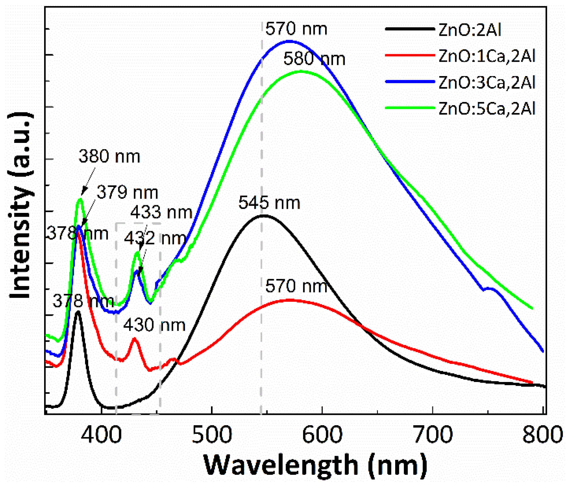
Photoluminescence spectroscopy was performed to measure and analyze the optical properties of Ca-doped ZnO:Al films, and the characteristic PL spectra are reported in Figure 4. The spectrum of ZnO:Al thin film has two main components: a narrow ultraviolet (UV) emission band (around 378 nm) and a broad visible emission band (at 545 nm) both obtained for 300 nm excitation wavelength, tabulated in Table 2. The first PL peak, situated in the UV range, corresponds to near-band-edge emission of ZnO and can be considered as excitonic emission, whereas the broad green emission indicates the presence of defects such as oxygen interstitial defects. Interestingly, the Ca-doped films display a modified green emission band compared to the reference (ZnO:Al 2%). In fact, the intensity of the green emission band is increased up to almost two times and the excitonic peak is increased also, which is another indicator for the modification of the crystal quality. In the present study, the green emission peak shifted from 545 nm (ZnO:Al 2%) to 580 nm (5% Ca-doped ZnO:Al 2%) which can be attributed to the influence of many factors such as addition of 1–5% concentration of Ca dopant and thermal treatment at 900 °C used for complete decomposition of Ca(OH)2. The broad and green PL emission band of the Ca doped films reveals that besides the direct band-to-band excitation, another emissive process takes place which is related to the localized states in the energy bandgap induced by Ca incorporation. A possible mechanism for this emission could be donor-acceptor recombination at the localized Ca-induced states [29]. Thus, certain energy states emerge during films deposition when the Ca content is increased. This increase in the electron concentration may be due to donor-like states, such as the [Zni] and [Vo+] states in the films [30]. Additionally, a new band appears around 430 nm for 1% Ca, 432 nm for 3% Ca and 433 for 5%. These results could be related to surface defects into the ZnO lattices. A new band group, centered at about 437 nm has been reported by Dhahri et al. [16] for the case of codoped ZnO:(Ca,Al) with 1 at.% of Al and different Ca (1–5 at.%) content synthesized by the sol-gel method and annealed at 400 °C for 2 h in air.
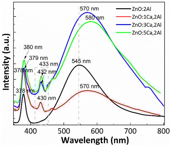
Figure 4.
PL Emission spectra of ZnO:Al 2% and Ca-doped ZnO:Al 2% thin films with: 1, 3 and 5% Ca.
Table 2.
PL Emission peaks and the excitonic energy (E0) of ZnO:Al 2% and Ca-doped ZnO:Al 2% thin films with: 1, 3 and 5% Ca.
3.4. Electrical Characterization
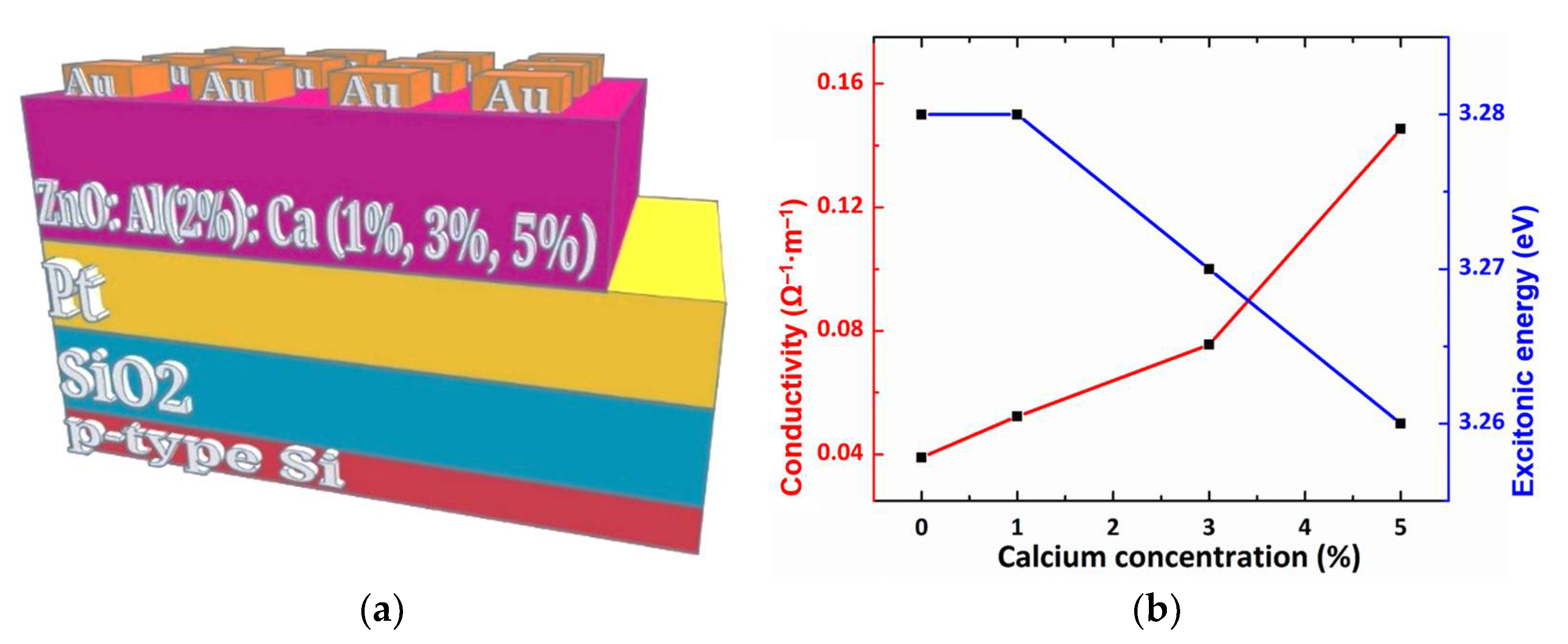
The effect of Ca doping on the electrical properties of ZnO:Al films, was studied by the electrical characterization of pure and doped ZnO:Al thin films at room temperature with a setup depicted in Figure 5a. The electrical conductivity (Figure 5b) was determined from I–V characteristic using the formula:
where σ is conductivity, R is electrical resistance, A is top electrode area and l is the thickness of thin film.
1\σ = R × (A\l)
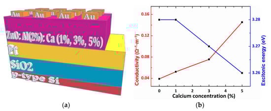
Figure 5.
(a) The set-up for the I–V measurements; (b) electrical conductivity and excitonic energy values as a function of calcium concentration of Ca doped ZnO: Althin films.
We obtained a value of electrical conductivity of 52 × 10−3 Ω−1·m−1 for the Ca-doped ZnO:Al sample with a concentration of 1% Ca, that is slightly increased compared to the value of electrical conductivity for the undoped ZnO: Al sample (39 × 10−3 Ω−1·m−1). An electrical conductivity value of 75 × 10−3 Ω−1·m−1 cm was obtained for 3% Ca concentration and 145 × 10−3 Ω−1·m−1 for 5% Ca concentration. In general, the electrical conductivity of ZnO at room temperature is due to the presence of intrinsic defects produced by oxygen vacancies. The electrical conductivity is determined by two factors: mobility and carrier concentration. The same electrical conductivity can come from the many electrons with a lower mobility or fewer electrons with a high level of mobility. On the other hand, a low level of doping concentration can lead to a reduction in mobility by the presence of defects which are responsible for the scattering [31]. In the case of doped ZnO systems it can be said that electrical conductivity is dominated by the presence of dopants and by the intrinsic defects induced during deposition. In this study, the doping concentration is low (≤5% Ca), and doping with Ca increases the density of defects, which can lead to a decrease in electrical conductivity. On the other hand, the presence of Al in a proportion of 2%, induces an increase in the number of free electrons in the system. In conclusion, it can be said that the electrical conductivity in the (Ca, Al) doped ZnO system is dependent on the proportion between the two dopants, Al and Ca.
4. Conclusions
Doped ZnO thin films with Al concentration fixed at 2 wt.% and varying Ca (1%, 3% and 5 wt.%) were successfully synthesized using RF magnetron sputtering followed by chemical diffusion. According to morpho-structural and optical investigations of our doped ZnO:Al thin films it was pointed that the concentration of Ca is a pivotal aspect in the determination of the main structural parameters and optical properties. For instance, different Ca concentration induces different dislocation density. Further, an increasing of the Ca concentration led to different PL emission spectra, affecting the broad green emission. At the same time, electrical properties are related to the doping and the microstructural parameters. Corroborating the electrical measurements with X-ray diffraction and optical measurements, one can infer that the electrical conductivity is dominated by intrinsic defects developed during deposition and by the existence of dopants. The possibility to tune the opto-electrical properties from doping/co-doping opens new pathways for designing of various optoelectronic devices.
Author Contributions
Conceptualization, A.-I.I., S.V., F.N. and L.M.V.; validation, F.N. and L.M.V.; formal analysis, I.M., C.R., O.T., and A.-I.I.; investigation, I.M., C.R., O.T. and A.-I.I.; resources, L.M.V.; data curation, A.-I.I.; writing—original draft preparation, A.-I.I.; writing—review and editing, A.-I.I., I.M., C.R., O.T., S.V., F.N. and L.M.V.; visualization, A.-I.I., I.M., C.R. and O.T.; supervision, F.N. and L.M.V.; project administration, L.M.V.; funding acquisition, L.M.V. All authors have read and agreed to the published version of the manuscript.
Funding
This work was supported by a grant of the Ministry of Research, Innovation and Digitization, CNCS/CCCDI – UEFISCDI, project number PN-III-P2-2.1-PED-2019-0841, within PNCDI III and by the National Core Programme-MICRO-NANO-SIS PLUS, 2019-2022, Cod: 1916.
Institutional Review Board Statement
Not applicable.
Informed Consent Statement
Not applicable.
Data Availability Statement
Data is contained within the article.
Conflicts of Interest
The authors declare no conflict of interest.
References
- Wang, Y.; Song, J.; Zhang, J.; Zheng, G.; Duan, X.; Xie, X.; Han, B.; Meng, X.; Yang, F.; Wang, G.; et al. Effect of substrate temperature on F and Al co-doped ZnO films deposited by radio frequency magnetron sputtering. Sol. Energy 2019, 194, 471–477. [Google Scholar] [CrossRef]
- Miyata, T.; Tokunaga, H.; Watanabe, K.; Ikenaga, N.; Minami, T. Photovoltaic properties of low-damage magnetron-sputtered n-type ZnO thin film/p-type Cu2O sheet heterojunction solar cells. Thin Solid Film. 2020, 697, 137825. [Google Scholar] [CrossRef]
- Carcia, P.F.; McLean, R.S.; Reilly, M.H.; Nunes, G. Transparent ZnO thin-film transistor fabricated by rf magnetron sputtering. Appl. Phys. Lett. 2003, 82, 1117–1119. [Google Scholar] [CrossRef]
- Liu, Y.; Zhu, S. Preparation and characterization of Mg, Al and Ga co-doped ZnO transparent conductive films deposited by magnetron sputtering. Results Phys. 2019, 14, 1–6. [Google Scholar] [CrossRef]
- Ebrahimifard, R.; Golobostanfard, M.R.; Abdizadeh, H. Sol-gel derived Al and Ga codoped ZnO thin films: An optoelectronic study. Appl. Surf. Sci. 2014, 290, 252–259. [Google Scholar] [CrossRef]
- Wietler, T.F.; Min, B.; Reiter, S.; Larionova, Y.; Reineke-Koch, R.; Heinemeyer, F.; Brendel, R.; Feldhoff, A.; Krugener, J.; Tetzlaff, D.; et al. High Temperature Annealing of ZnO:Al on Passivating POLO Junctions: Impact on Transparency, Conductivity, Junction Passivation, and Interface, Stability. IEEE J. Photovolt. 2019, 9, 89–96. [Google Scholar] [CrossRef] [Green Version]
- Mahdhi, H.; Ben Ayadi, Z.; Djessas, K. Physical properties of metal-doped ZnO thin films prepared by RF magnetron sputtering at room temperature. J. Solid State Electrochem. 2019, 23, 3217–3224. [Google Scholar] [CrossRef]
- Lee, W.; Shin, S.; Jung, D.R.; Kim, J.; Nahm, C.; Moon, T.; Park, B. Investigation of electronic and optical properties in Al-Ga codoped ZnO thin films. Curr. Appl. Phys. 2012, 12, 628–631. [Google Scholar] [CrossRef]
- Tsay, C.-Y.; Pai, K.-C. Properties of Al-Ga co-doped ZnO semiconductor thin films deposited on polyethylene terephthalate substrates by radio frequency magnetron sputtering. Thin Solid Film. 2018, 654, 11–15. [Google Scholar] [CrossRef]
- Correia, F.C.; Ribeiro, J.M.; Kuzmin, A.; Pudza, I.; Kalinko, A.; Welter, E.; Mendes, A.; Rodrigues, J.; Ben Sedrine, N.; Monteiro, T.; et al. The role of Ga and Bi doping on the local structure of transparent zinc oxide thin films. J. Alloy. Compd. 2021, 870, 159489. [Google Scholar] [CrossRef]
- Sun, H.; Chen, S.-C.; Wang, C.-H.; Lin, Y.-W.; Wen, C.-K.; Chuang, T.-H.; Wang, X.; Lin, S.-S.; Dai, M.-J. Electrical and magnetic properties of (Al, Co) co-doped ZnO films deposited by RF magnetron sputtering. Surf. Coat. Technol. 2019, 359, 390–395. [Google Scholar] [CrossRef]
- Wang, F.-H.; Chang, C.-L. Effect of substrate temperature on transparent conducting Al and F co-doped ZnO thin films prepared by rf magnetron sputtering. Appl. Surf. Sci. 2016, 370, 83–91. [Google Scholar] [CrossRef]
- Zhu, Y.Z.; Chen, G.D.; Ye, H.G.; Walsh, A.; Moon, C.Y.; Wei, S.H. Electronic structure and phase stability of MgO, ZnO, CdO, and related ternary alloys. Phys. Rev. B 2008, 77, 245209-1–245209-7. [Google Scholar] [CrossRef] [Green Version]
- Kwon, J.H.; Jeon, Y.; Choi, K.C. Robust transparent and conductive gas diffusion multibarrier based on Mg- and Al-doped ZnO as Indium tin oxide-free electrodes for organic electronics. ACS Appl. Mater. Inter. 2018, 10, 32387–32396. [Google Scholar] [CrossRef] [PubMed]
- Zhang, H.; Li, W.; Qin, G.; Ruan, H.; Huang, Z.; Wu, F.; Kong, C.; Fang, L. Role of zinc interstitial defects in indium and magnesium codoped ZnO transparent conducting films. Appl. Surf. Sci. 2019, 492, 392–398. [Google Scholar] [CrossRef]
- Dhahri, R.; Leonardi, S.G.; Hjiri, M.; El Mir, L.; Bonavita, A.; Donato, N.; Iannazzo, D.; Neri, G. Enhanced performance of novel calcium/aluminum co-doped zinc oxide for CO2 sensors. Sens. Actuators B Chem. 2017, 239, 36–44. [Google Scholar] [CrossRef]
- Visali, P.; Bhuvaneswari, R. Photoluminescence and enhanced photocatalytic activity of ZnO nanoparticles through incorporation of metal dopants Al and Ca. Optik 2020, 202, 1–7. [Google Scholar] [CrossRef]
- Kaźmierczak-Bałata, A.; Bodzenta, J.; Guziewicz, M. Microscopic investigations of morphology and thermal properties of ZnO thin films grown by atomic layer deposition method. Ultramicroscopy 2020, 210, 1–7. [Google Scholar] [CrossRef] [PubMed]
- Ivanova, T.; Harizanova, A.; Koutzarova, T.; Vertruyen, B.; Closset, R. Structural and optical characterization of nitrogen and gallium co-doped ZnO thin films, deposited by sol-gel method. J. Mol. Struct. 2020, 1206, 1–11. [Google Scholar] [CrossRef]
- Ravichandran, K.; Jansi Santhosam, A.; Sridharan, M. Effect of tungsten doping on the ammonia vapour sensing ability of ZnO thin films prepared by a cost effective simplified spray technique. Surf. Interfaces 2020, 18, 1–11. [Google Scholar] [CrossRef]
- Drewelow, G.; Song, H.W.; Jiang, Z.-T.; Lee, S. Factors controlling conductivity of PEDOT deposited using oxidative chemical vapor deposition. Appl. Surf. Sci. 2020, 501, 1–8. [Google Scholar] [CrossRef]
- Vasin, A.V.; Rusavsky, A.V.; Bortchagovsky, E.G.; Gomeniuk, Y.V.; Nikolenko, A.S.; Strelchuk, V.V.; Yatskiv, R.; Tiagulskyi, S.; Prucnal, S.; Skorupa, W.; et al. Methane as a novel doping precursor for deposition of highly conductive ZnO thin films by magnetron sputtering. Vacuum 2020, 174, 1–6. [Google Scholar] [CrossRef]
- Andolsi, Y.; Chaabouni, F. Optoelectronic properties of Cr doped ZnO thin films deposited by RF magnetron sputtering using a powder target. J. Alloy. Compd. 2020, 818, 1–8. [Google Scholar] [CrossRef]
- Han, Y.; Yang, T.; Chen, Y. A perspective on morphology controlled synthesis of powder by tuning chemical diffusion and reaction. Adv. Powder Technol. 2019, 31, 922–925. [Google Scholar] [CrossRef]
- Otieno, F.; Airo, M.; Ganetsos, T.; Erasmus, R.M.; Billing, D.G.; Quandt, A.; Wamwangi, D. Role of oxygen concentrations on structural and optical properties of RF magnetron sputtered ZnO thin films. Opt. Quant. Electron. 2019, 51, 359. [Google Scholar] [CrossRef]
- Patterson, A.L. The Scherrer Formula for X-Ray Particle Size Determination. Phys. Rev. 1939, 56, 978–982. [Google Scholar] [CrossRef]
- Waseda, K.; Matsubara, Y.; Shinoda, E. X-ray Diffraction Crystallography, 1st ed.; Springer: Berlin, Germany, 2011. [Google Scholar] [CrossRef]
- Lee, J.K.; Park, S.; Ryu, B.; Lee, H.S.; Park, J.; Park, S. Effect of defect interactions with interstitial Ag in the lattice of BixSb2−xTe3 alloys and their thermoelectric properties. Appl. Phys. Lett. 2021, 118, 052102. [Google Scholar] [CrossRef]
- Wu, P.; Zhong, J.; Emanetoglu, N.W.; Chen, Y.; Muthukumar, S.; Lu, Y. Diffusion in epitaxial (1120) ZnO thin films. J. Electron. Mater. 2004, 33, 596–599. [Google Scholar] [CrossRef]
- Lu, Y.-F.; Lan, W.-H.; Wang, M.-C.; Shih, M.-C.; Kuo, H.-H.; Feng, D.J.-Y.; Chiu, Y.-J.; Hung, Y., Jr.; Yang, C.-F. Carrier concentration of calcium zinc oxide with different calcium contents deposited through spray pyrolysis. Microsyst. Technol. 2018, 24, 4267–4272. [Google Scholar] [CrossRef]
- Simimol, A.; Anappara Aji, A.; Barshilia, H.C. Influence of defects on electrical properties of electrodeposited co-doped ZnO nanocoatings. Mater. Res. Express 2017, 4, 1–11. [Google Scholar] [CrossRef]
Publisher’s Note: MDPI stays neutral with regard to jurisdictional claims in published maps and institutional affiliations. |
© 2021 by the authors. Licensee MDPI, Basel, Switzerland. This article is an open access article distributed under the terms and conditions of the Creative Commons Attribution (CC BY) license (https://creativecommons.org/licenses/by/4.0/).