Article

Hetero-Epitaxial Growth of AlN Deposited by DC Magnetron Sputtering on Si(111) Using a AlN Buffer Layer

1
Laboratoire Microstructures et Défauts dans les Matériaux, Université Frères Mentouri Constantine 1, Route Ain El Bey, Constantine 25017, Algeria
2
Institut des Matériaux Jean Rouxel IMN UMR 6502, Université de Nantes, 2 rue de La Houssinière BP 32229, CEDEX, 44322 Nantes, France
3
Département de Pharmacie, Faculté de Médecine, Université Constantine 3, Nouvelle ville Ali Mendjeli 25016, Algeria
*
Authors to whom correspondence should be addressed.
Coatings 2021, 11(9), 1063; https://doi.org/10.3390/coatings11091063
Submission received: 13 July 2021 / Revised: 20 August 2021 / Accepted: 23 August 2021 / Published: 3 September 2021
(This article belongs to the Section Thin Films)

Abstract

:
This paper reports the effect of Silicon substrate orientation and Aluminum nitride buffer layer deposited by molecular beam epitaxy on the growth of aluminum nitride thin films deposited by a DC magnetron sputtering technique at low temperatures. The structural analysis has revealed a strong (0001) fiber texture for both Si(100) and (111) substrates, and a hetero-epitaxial growth on a AlN buffer layer, which is only a few nanometers in size, grown by MBE onthe Si(111) substrate. SEM images and XRD characterization have shown an enhancement in AlN crystallinity. Raman spectroscopy indicated that the AlN film was relaxed when it deposited on Si(111), in compression on Si(100) and under tension on a AlN buffer layer grown by MBE/Si(111) substrates, respectively. The interface between Si(111) and AlN grown by MBE is abrupt and well defined, contrary to the interface between AlN deposited using PVD and AlN grown by MBE. Nevertheless, AlN hetero-epitaxial growth was obtained at a low temperature (<250 °C).

1. Introduction

Aluminum nitride (AlN) thin films can be a promising candidate in optical, mechanical, and electronic applications. It can serve as a semiconductor when doped [1] and also as a passivation layer for semiconductors [2]. Besides, AlN thin films are integrated in surface acoustic wave (SAW) devices, where they insure high frequency ranges, a large electromechanical coupling factor ( K s 2 ), and temperature stability of the respective device. Nevertheless, the quality of these integrated films has a strong impact on the performance of the SAW devices [3,4]. The film properties depend not only on the crystal structure of AlN, but alsoon its preferential orientation [5], the c-axis of the wurtzite AlN structure in our case. The films can be composed of multiple crystal orientations scored (002), (100) etc. AlN thin films are grown using physical vapor deposition (PVD) on several substrates such as silicon (Si) [6], sapphire [7], and indium phosphide (InP) [8].
To realize an epitaxial growth of AlN thin films, the Si substrates have been extensively regarded because of their large scale and easiness to carry out industrial mass production [9]. Nevertheless, it is very difficult to achieve the epitaxial growth of AlN thin films deposited on Si substrates by PVD methods, in particular at low temperatures, owing to the lattice mismatch and different coefficient of thermal expansion between AlN film and Si substrates, which will lead to a high density of defects to AlN thin films layers [10,11]. Furthermore, depositing AlN layers on Si simplify the process and the device structure for a low cost [12].
Currently, a lot of research works have been proposed in the domain of AlN epitaxial films synthesized on both (100) and (111) Si substrates to reach the high quality of AlN films. Liegen Huang et al. [13] reported the epitaxial growth of AlN films grown on Si substrates by metal organic chemical vapor deposition (MOCVD) by enhancing the Si substrate surface by changing the concentration of HF solutions. Holger Fiedler et al. [14] investigated the effect of long-term stability on the interface between AlN films and silicon for microwave frequency electronic devices [14]. The effect of substrate temperature, ammonia (NH3), flow rate, and layer thickness on the characteristics of AlN layers was reported [15,16]. In the literature, most investigators concentrate on the optimization of the growth parameters. On the other hand, the optimization of the Si substrate is rarely investigated.
In fact, the Si substrate surface has an impact on the epitaxial growth of AlN, as the chemical contaminants and particulate impurities on the Si surface influence the characteristic of AlN films, and also the device performance and the yield [13,17,18]. For that, the Si surface condition is very important. Generally, the wet etching method is used to clean the Si substrate surface [19,20,21]. The impact of the Si substrate surface on the epitaxial growth of AlN was studied [13], but, unfortunately, the mechanism is still not clear. K. Ait Aissa et al. [22] showed that the interface between the AlN film and the Si(100) substrate is abrupt, which indicates a local epitaxial growth of AlN on Si(100) deposited by high-power impulse magnetron sputtering (HiPIMS), However, an amorphous intermediate layer was seen in the case of the AlN film grown on Si(100) by direct current magnetron sputtering (DCMS).
In this study, the quality of AlN thin films deposited by DCMS was investigated. We report on the growth of AlN films deposited at low temperatures on Si(100), Si(111), and on a 1-nm composite substrate of AlN buffer layer deposited by molecular beam epitaxy (MBE) on Si(111). Special attention was given to the effect of the AlN buffer layer on the epitaxial growth and quality of AlN films deposited by DCMS.

2. Materials and Methods

AlN films, with ~600 nm thickness, were deposited on different substrates using a DCMS technique with the AV01 reactor. Before the deposition, the silicon (100) and (111) substrates were ultrasonically cleaned in both acetone and ethanol solvents, and then dried under nitrogen gas flow. An 8″ target was used, consisting of 99.99 pure aluminum (Al) water-cooled magnetron cathode. The sputtering system used to deposit AlN films was a Pinnacle Plus + 5kW® DC power supply, with a power of 1800 W DC power supply. The system was pumped to a base pressure of 3 × 10⁻⁵ Pa using a turbo molecular pump prior to introducing argon (Ar) and nitrogen (N2) gases. The distance between the target and substrate holder was 37 mm. The temperature during the deposition was <250 °C. The target was cleaned before deposition using Ar gas discharge followed by a pre-sputtering step using the same conditions as the subsequent film deposition with a shutter shielding the sample in order to remove surface oxidation of the target. The sputtering pressure was fixed at 0.3 Pa. The reactive N2 gas was fixed at 55%. The silicon substrate temperature was about 150 °C during the growth, as measured by the thermal couple, which was fixed to the substrate holder.
In order, to realize the epitaxial growth of AlN, we proposed to cover the substrate by a 1-nm-thick AlN deposited by molecular beam epitaxy MBE on HF-cleaned 2-in.-diameter Si(111) substrates. After hydrogen desorption at 700 °C under high vacuum (~10−8 mbar), the nucleation process was initiated at 600–650 °C before grading the substrate temperature for growing the rest of the film at 920 °C. The buffer layer’s thickness was measured by the reflection high-energy electron diffraction (RHEED) method [23,24,25].
The crystal structures of AlN films were investigated by X-ray diffraction (XRD) using a PANanalytical Empyrean® X-ray diffractometer (Malvern Panalytical, Malvern, UK), with Cu Kα radiation (λ = 0.154 nm), voltage and current (40 kV-40 mA), respectively, as described early by B. Riah et al. [26]. In addition, The reflection spectra of the respective molecular structure for the prepared AlN films were identified, studied and presented using Raman spectrometer (Horiba Jobin-Yvon lab-RamT64000®, Horiba, Kyoto, Japan), in backscattering z(x, unpolarised)z, configuration, with z orthogonal to the substrate surface and utilizing the 514 nm lines of a (Cd-He) green laser as the excitation source at room temperature. Furthermore, Raman spectroscopy was used in order to obtain the quality of the deposited films and calculate the residual stress which was developed after deposition. Moreover, scanning electron microscopy (SEM) (Jeol, Tokyo, Japan) and the high-resolution transmission electron microscopy (HRTEM) (Hitachi, Marunouchi, Tokyo, Japan) were used in order to thoroughly study the films of the micro-structure, the morphology, and the interfaces between the layers. The HRTEM is used only in the case of the AlN deposited on AlN MBE/Si(111).
A DEKTAK VEECO 8 profilometer was used to estimate the thickness and residual stresses of the films by measuring the substrate curvature before and after deposition [27].
σ = E 6   ( 1 υ ) t s 2 t f ( 1 r c 1 r u )
where:
  • σ is the stress on GPa.
  • E is the Young’s module of the substrate in GPa.
  • υ is the Poisson’s ration for the silicon substrate.
  • ts is the silicon thickness in m.
  • tf is the film thickness in m.
  • rc the radius of curvature of the substrates before AlN deposition in m.
  • ru are the radius of curvature of the substrates after AlN deposition in m.
However, the measurement of substrates radius curvature was very significant in order to estimate the internal stress of the film. The thickness was derived from the difference in height between a first area coated with the deposited film and a second which was previously hidden during deposition. Moreover, the residual stress data were coupled with Raman shifts. The variation of the stress as function of the ( E 2 H ) band shift was linear, as represented in Figure 1 [28]. For a given position of E2 band, the residual stress was easily deduced.

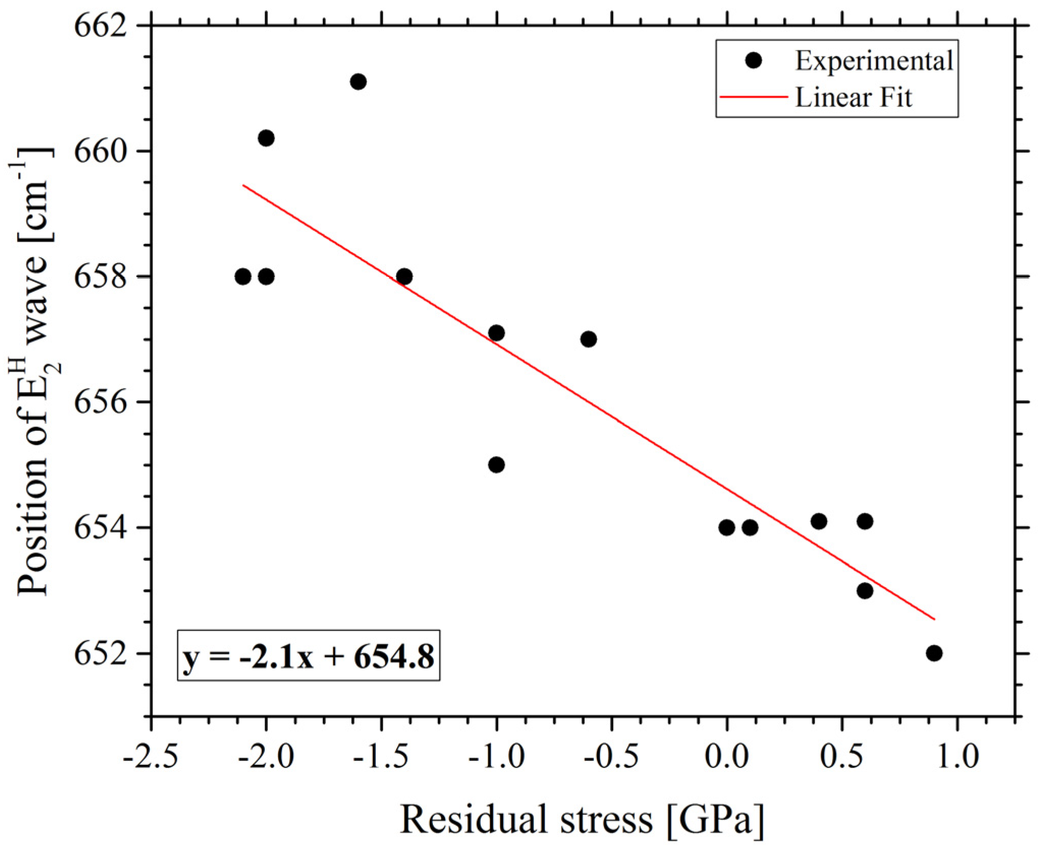
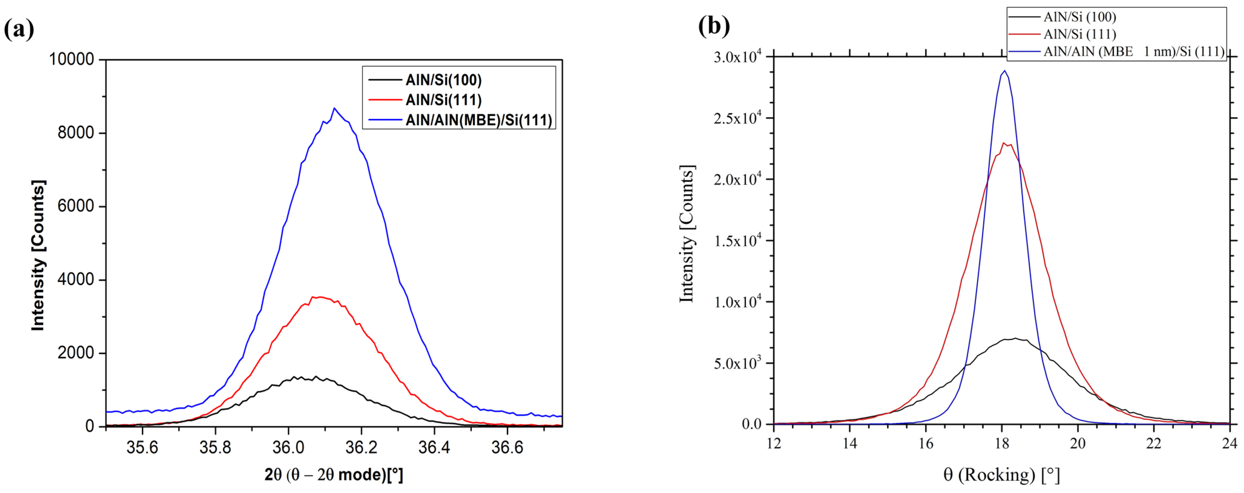
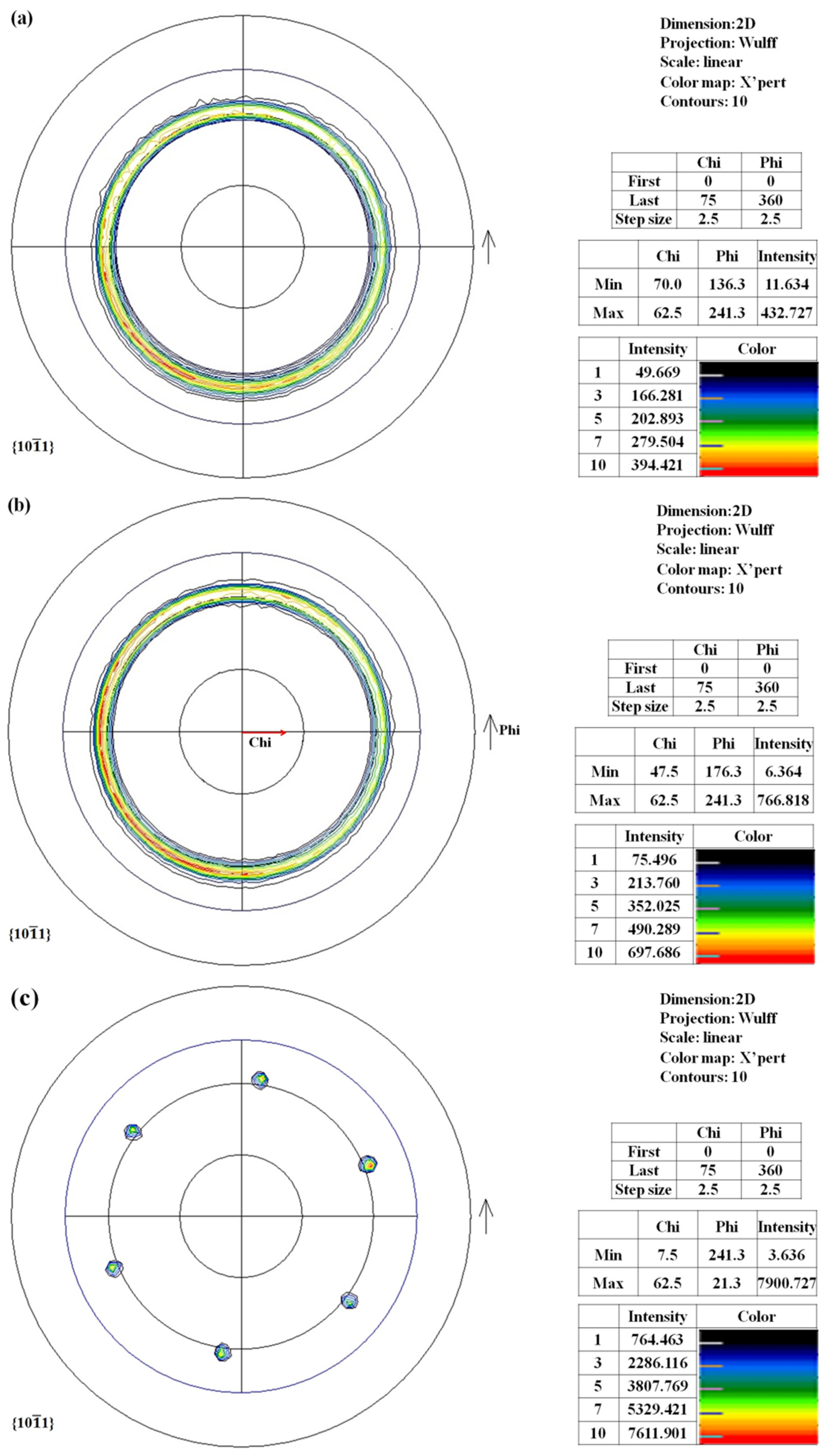
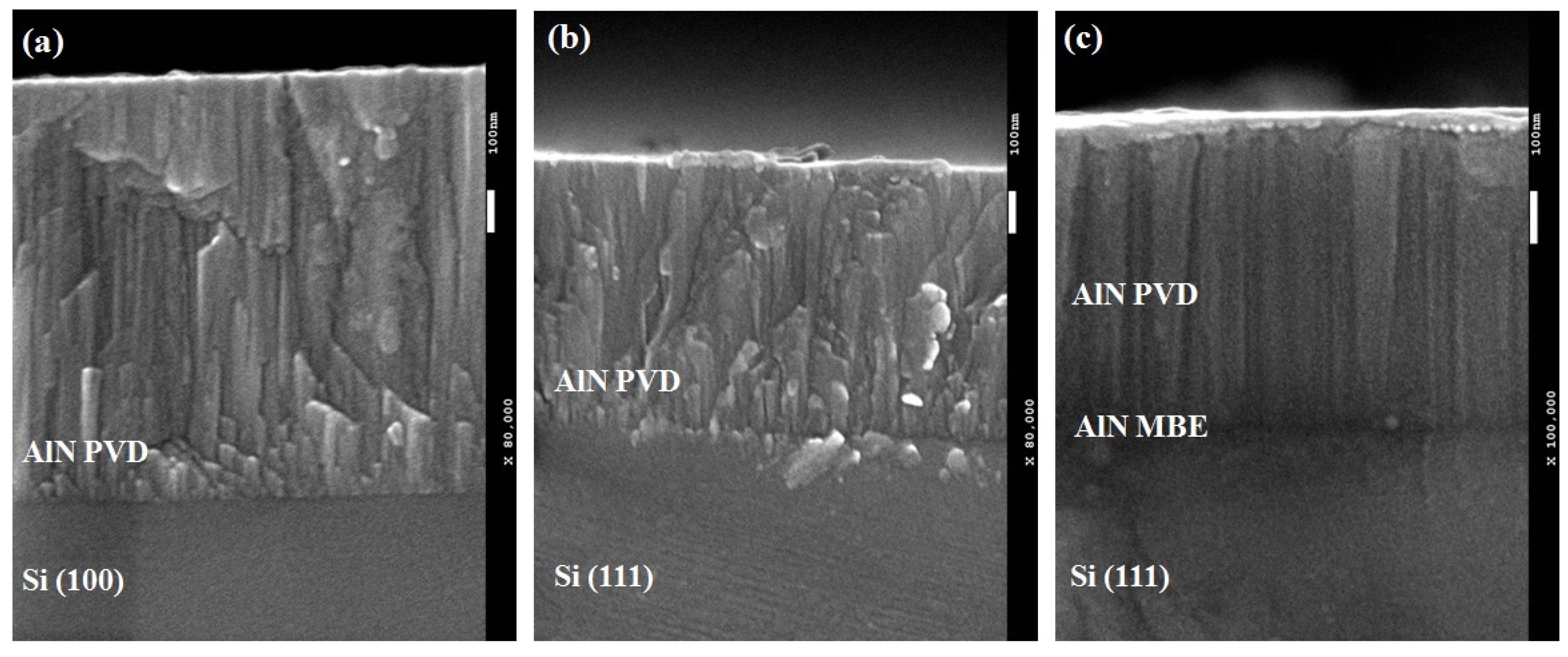
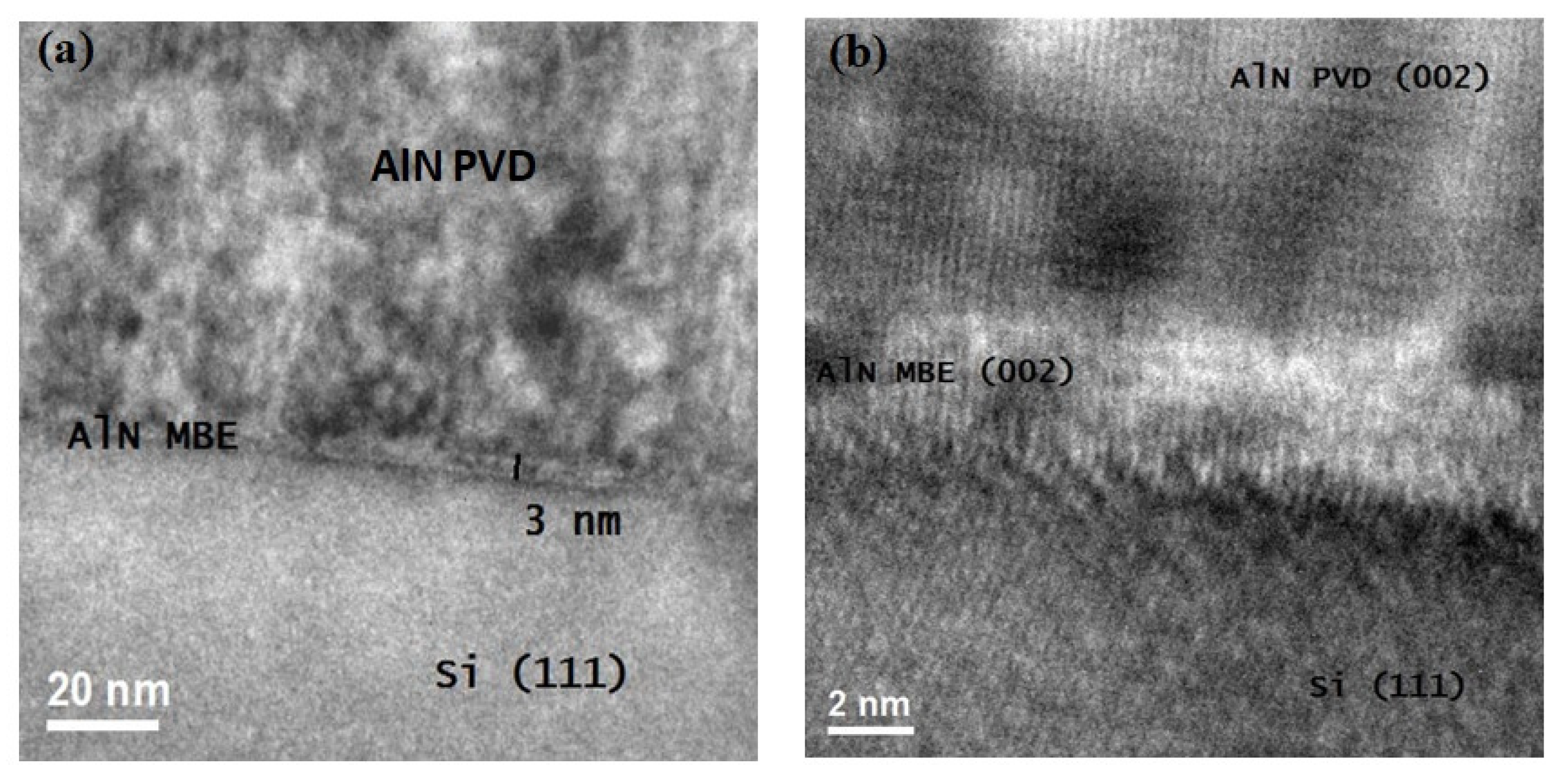
3. Results and Discussion

The XRD patterns of the θ-2θ (Bragg-Brentano Geometry) and the θ-θ scans of AlN/Si(100), AlN/Si(111), and AlN/AlN MBE (1 nm)/Si(111) are shown in Figure 2a,b, respectively. The highest intensity of the (002) reflection indicates an oriented growth along the c-axis perpendicular to substrate for all samples, which is ascribed to wurtzite-type hexagonal structure. The measure of peak width and the full width at half maximum of the X-ray rocking curve (RC-FWHM) for determining the quality of the film (Gaussian curve) shows that the FWHM values decreases from 3.2° for AlN/Si(100) to 2.3° in the case of AlN/Si(111). This result indicates that the quality of AlN films improves depending on the Si orientation. The enhancement is due to the lattice mismatch which is very important in the case of Si(100) compared to that in Si(111). On the other hand, the diffraction peak intensity of the (0002) AlN increases and the RC-FWHM of the AlN film decreases from 2.3° to 1.2° using the AlN (MBE) interlayer; this can indicate that the use of a AlN buffer layer enhances the crystalline quality of AlN film and facilitates its deposition. In the case of AlN deposited on a AlN buffer layer on Si(111), the peak position of the (0002) plan is 2θ = 36.15°. An evident shift of this peak toward lower angles with the film deposited directly on both Si(100) and (111) is observed. This may be due to the stress effect within the film. The shift of (0002) peak in the case of AlN deposited on Si(111), where 2θ = 36.09°, is less important compared to the film deposited on Si(100), where 2θ = 36.04°.
To understand this change, XRD pole figures (0001), {10 1 ¯ 1}, {10 1 ¯ 2} and {10 1 ¯ 3} of hexagonal AlN were obtained [26], but only the pole figures {10 1 ¯ 1} and {10 1 ¯ 2} are used in this study. The {10 1 ¯ 1} pole figures of AlN/Si(100), AlN/Si(111), and AlN/AlN MBE/Si(111) films are shown in Figure 3a–c, respectively. For both AlN/Si(100) and AlN/Si(111) samples, the {10 1 ¯ 1} pole figures intensity maxima are distributed along a ring located at χ = 62.5°, demonstrating the presence of a polycrystalline film with a (0001) strong fiber-texture, where the grains of the film are composed of one family of parallel planes at the substrate’s surface with an axis of rotation around the normal of these planes. Moreover, the ring at χ = 62.5° caused by the {10 1 ¯ 1} facets implies that no preferred in-plane orientation is formed for both cases. However, in the case of AlN deposited on AlN (MBE) /Si(111), the {101 1 ¯ } pole figure shows a maximum intensity with a six-fold symmetry at χ = 62.5°. This confirms that the AlN thin film deposited on AlN /Si(111) does not have a fiber texture any more, but has grown epitaxially on the AlN /Si(111) substrate.
The morphological and cross sectional characterization of AlN films synthesized at different substrates, i.e., Si(100), Si(111), and AlN buffer layer/Si(111), were realized using SEM analysis. Figure 4 shows the cross-section SEM images for the three samples synthesized. The AlN layer shows several columnar grains which are perpendicular to the substrate surface for all samples, and for fairly similar thicknesses. The AlN film deposited by DCMS does not show any meaningful change in the film morphology for both (100) and (111) Si substrates. However, it can be noted that the AlN film deposited on AlN MBE/Si(111) has the best columnar crystalline compared to those deposited on both Si(100) and Si(111) substrates.
Figure 5 represents the Raman spectra collected at room temperature from all samples. The peaks that are situated at approximately 604 cm−1 (and 655.57 cm−1) for AlN DCMS/Si(100), 654.86 cm−1 for AlNDCMS/Si(111), and 648 cm−1 for AlNDCMS/AlNMBE/Si(111)) are attributed to the A1(TO) and E2 (high) Raman mode of AlN, respectively [29] (TO corresponds to transversal optical phonons). The E2 (high) peak became broader in the case of the film AlN deposited by DCMS on a AlN buffer layer on Si(111). The expansion of the E2 (high) peak may be related to the crystalline deterioration or to the intrinsic stress [30]. However, as the XRD results (Figure 2a,b) validate the high crystalline quality of the AlN deposited films on the AlN buffer layer on Si(111), the theory of crystalline deterioration can be excluded. It can be seen from Figure 5 that the AlN film deposited on the Si(111) substrate is almost relaxed (stress = 0.03 GPa). Nevertheless, for AlN deposited on Si(100), the stress is equal to −0.37 GPa, meaning that the film is in compression. The residual stresses in the films deposited by PVD methods comes from the intrinsic stresses due to defects, lattice mismatch stresses, and thermal residual stress due to coefficient thermal expansion mismatches between substrates and the deposited films. The defects in the deposited AlN films are complex, such as vacancies, dislocations, grain boundary density of the film, impurities, and surface atomic arrangements of the substrates. As both the atomic arrangements of Si(111) surface and AlN (0002) oriented films are hexagonal, vertical columnar growth of the AlN film is observed with minimal residual stress [31,32]. On the other hand, AlN films deposited on the AlN buffer layer/Si(111) have shown a stress of 3.23 GPa. This result indicates that the film is under tension, which is in good agreement with XRD results.
The interfacial between the AlN film and the silicon substrate is very important to achieve the epitaxial growth of AlN sputtered films [13]. In order to further study the interfacial between AlN films deposited by DMCS grown on the AlN buffer layer on Si(111) substrates, TEM characterizations are investigated. The TEM cross section image of AlN deposited on 1 nm of AlN MBE/Si(111) by DCMS is shown in Figure 6a. The presence of a 3-nm continuous layer between the AlN deposited by DCMS and AlN buffer layer can be seen; this 3-nm layer corresponds to the 1-nm AlN buffer layer, as the thickness measurement of the buffer layer was made by RHEED technique, as well as the 2-nm interfacial AlN deposited by DCMS method. The interface between AlN MBE and Si(111) is abrupt, which means that there is a discontinuity of the composition between the AlN buffer layer and Si(111) on weak thicknesses from 0.2 to 0.5 nm. On the other hand, that there is a good continuity at the interface between the AlN film deposited by DCMS and AlN buffer layer, which can show the presence of defects. Furthermore, a dense structure is highlighted for AlN film deposited by DCMS [33].
Figure 6b represents a HRTEM image of the AlN deposited on AlNMBE on Si(111). The AlN film deposited by DCMS method exhibits very beautiful planes, some of which are perfectly matched. However, in some parts, there is a lake in continuity. This can be attributed to the ionic bombardment, which can be enough to eliminate a part of the AlN buffer layer deposited by molecular beam epitaxy MBE [22]. It is noteworthy to mention that the DCMS method is a subsurface method [34]. This proves that the heteroepitaxial growth of AlN deposited on Si(111) was achieved using a 1-nm AlN buffer layer deposited by molecular beam epitaxy.

4. Conclusions

In this study, a hetero epitaxial growth of AlN films deposited by DCMS was obtained using a 1-nm AlN buffer layer grown on Si(111) by molecular beam epitaxy. The effect of the buffer layer on the quality of AlN hetero epitaxial film was carefully studied by various methods. The crystallinity of AlN layers was improved using a 1-nm AlN buffer layer. The FWHM’s of the (0002) X-ray rocking curves were decreased using an AlN buffer layer. The XRD pole figures revealed a strong (0001) fiber texture for both (100) and (111) Si substrates and a hetero-epitaxial growth in the case of AlN deposited by DCMS on AlN buffer layer on Si(111).The SEM cross section images indicate that the AlN film deposited on AlN MBE/Si(111) has the best columnar crystalline compared to those deposited on both Si(100) and (111) substrates. The Raman spectroscopy indicated that the film AlN is relaxed in compressive stress and under tension when it was deposited on Si(111), Si(100), and AlN buffer layer, respectively. HRTEM confirmed that the heteroepitaxial growth of AlN deposited by DCMS was reached using a 1-nm AlN buffer layer deposited by molecular beam epitaxy.

Author Contributions

Conceptualization, B.R. and M.R.; methodology, B.R., M.R., A.A., N.R.; software, B.R. and M.R.; validation, M.A.D.; formal analysis, B.R., M.R. and J.C.; investigation, J.C.; resources, J.C. and M.A.D.; data curation, B.R.; writing—original draft preparation, B.R. and M.R.; writing—review and editing, R.Z., J.C., A.A., M.A.D.; visualization; supervision, M.A.D.; project administration; funding acquisition. All authors have read and agreed to the published version of the manuscript.

Funding

This work was financially supported in part by the European Union’s Horizon 2020 Research and Innovation Program (Grant agreement: n 644453).

Institutional Review Board Statement

Not applicable.

Informed Consent Statement

Not applicable.

Data Availability Statement

Data is contained within the article.

Acknowledgments

The financial support of DGRSDT is strongly acknowledged.

Conflicts of Interest

The authors declare no conflict of interest.

References

  1. Xiong, J.; Guo, P.; Guo, F.; Sun, X.; Gu, H. Room temperature ferromagnetism in Mg-doped AlN semiconductor films. Mater. Lett. 2014, 117, 276–278. [Google Scholar] [CrossRef]
  2. Aubry, R.; Michel, N.; Jacquet, J.C.; Baczkowski, L.; Patard, O.; Chartier, E.; Semmar, N. S3-P11: Thin-film coatings for improved thermal performances of GaN-based HEMTs. In 2014 Lester Eastman Conference on High Performance Devices (LEC); IEEE: Providence, RI, USA, 2014. [Google Scholar] [CrossRef]
  3. Rodríguez-Madrid, J.G.; Iriarte, G.F.; Araujo, D.; Villar, M.P.; Williams, O.A.; Müller-Sebert, W.; Calle, F. Optimization of AlN thin layers on diamond substrates for high frequency SAW resonators. Mater. Lett. 2012, 66, 339–342. [Google Scholar] [CrossRef] [Green Version]
  4. Clement, M.; Vergara, L.; Sangrador, J.; Iborra, E.; Sanz-Hervas, A. SAW characteristics of AlN films sputtered on silicon substrates. Ultrasonics 2004, 42, 403–407. [Google Scholar] [CrossRef]
  5. Ishiharaa, M.U.; Lia, S.J.; Yumotoa, H.; Akashib, K.; Idec, Y. Control of preferential orientation of AlN films prepared by the reactive sputtering method. Thin Solid Film. 1998, 316, 152–157. [Google Scholar] [CrossRef]
  6. Shukla, G.; Khare, A. Dependence of N2 pressure on the crystal structure and surface quality of AlN thin films deposited via pulsed laser deposition technique at room temperature. Appl. Surf. Sci. 2008, 255, 2057–2062. [Google Scholar] [CrossRef]
  7. Sudhir, G.S.; Fujii, H.; Wong, W.S.; Kisielowski, C.; Newman, N.; Dieker, C.; Liliental-Weber, Z.; Rubin, M.D.; Weber, E.R. Pulsed laser deposition of aluminum nitride and gallium nitride thin films. Appl. Surf. Sci. 1998, 127–129, 471–476. [Google Scholar] [CrossRef]
  8. Bhattacharya, P.; Dwarka, N. Bose, laser deposition of AlN thin films on InP and GaAs. Jpn. J. Appl. Phys. 1991, 30, L1750. [Google Scholar] [CrossRef]
  9. Sergeeva, O.N.; Bogomolov, A.A.; Solnyshkin, A.V.; Komarov, N.V.; Kukushkin, S.A.; Krasovitsky, D.M.; Dudin, A.L.; Kiselev, D.A.; Ksenich, S.V.; Senkevich, S.V. SEM, dielectric, pyroelectric, and piezoelectric response of thin epitaxial AlN films grown on SiC/Si substrate. Ferroelectrics 2015, 477, 121–130. [Google Scholar] [CrossRef]
  10. Kukushkin, S.A.; Osipov, A.V.; Sergeeva, O.N.; Kiselev, D.A.; Bogomolov, A.A.; Solnyshkin, A.V.; Kaptelov, E.Y.; Senkevich, S.V.; Pronin, I.P. yroelectric and piezoelectric responses of thin AlN films epitaxy-grown on a SiC/Si substrate. Phys. Solid State 2016, 58, 967–970. [Google Scholar] [CrossRef]
  11. Kurose, N.; Ozeki, K.; Araki, T.; Iwata, N. Realization of conductive. In Proceedings of the 2016 Compound Semiconductor Week (CSW) [Includes 28th International Conference on Indium Phosphide & Related Materials (IPRM) & 43rd International Symposium on Compound Semiconductors (ISCS), Toyama, Japan, 26–30 June 2016. [Google Scholar]
  12. AitAissa, K.; Achour, A.; Elmazria, O.; Simon, Q.; Elhosni, M.; Boulet, P.; Robert, S.; Djouadi, M.A. AlN films deposited by dc magnetron sputtering and high power impulse magnetron sputtering for SAW applications. J. Phys. D Appl. Phys. 2015, 48, 145307. [Google Scholar] [CrossRef]
  13. Huang, L.; Li, Y.; Wang, W.; Li, X.; Zheng, Y.; Wang, H.; Zhang, Z.; Li, G. Growth of high-quality AlN epitaxial film by optimizing the Si substrate surface. Appl. Surf. Sci. 2018, 435, 163–169. [Google Scholar] [CrossRef]
  14. Fiedler, H.; Leveneur, J.; Nancarrow, M.; Mitchell, D.R.G.; Kennedy, J. Effect of long-term stability of the aluminium nitride—Silicon interface for microwave-frequency electronic devices. Appl. Surf. Sci. 2021, 551, 149461. [Google Scholar] [CrossRef]
  15. Harumoto, T.; Sannomiya, T.; Muraishi, S.; Rong, T.U.; Lianmeng, Z.; Nakamura, Y.; Shi, J. Effect of substrate temperature on the structure and magnetic properties of CoPt/AlN multilayer films. J. Wuhan Univ. Technol.-Mater. Sci. Ed. 2016, 31, 44–47. [Google Scholar]
  16. Çörekçi, S.; Öztürk, M.K.; Çakmak, M.; Özçelik, S.; Özbay, E. The influence of thickness and ammonia flow rate on the properties of AlN layers. Mater. Sci. Semicon. Proc. 2012, 15, 32–36. [Google Scholar] [CrossRef] [Green Version]
  17. Huck, L.A.; Buriak, J.M. Toward a mechanistic understanding of exciton-mediated hydrosilylation on nano crystalline silicon. J. Am. Chem. Soc. 2012, 134, 489–497. [Google Scholar] [CrossRef]
  18. Kern, W. Overview and evolution of silicon wafer cleaning technology. Handb. Silicon Wafer Clean. Technol. 2008, 3–85. [Google Scholar] [CrossRef]
  19. Yang, H.; Wang, W.; Liu, Z.; Li, G. Homogeneous epitaxial growth of AlN single-crystalline films on 2 inch-diameter Si(111) substrates by pulsed laser deposition. CrystEngComm 2013, 36, 15. [Google Scholar] [CrossRef]
  20. Sharofidinov, S.S.; Nikolaev, V.I.; Smirnov, A.N.; Chikiryaka, A.V.; Nikitina, I.P.; Odnoblyudov, M.A.; Bugrov, V.E.; Romanov, A.E. On a reduction in cracking upon the growth of AlN on Si substrates by hydride vapor-phase epitaxy. Semicond 2016, 50, 541–544. [Google Scholar] [CrossRef]
  21. Imran, S.; Yuan, J.; Yin, G.; Ma, Y.; He, S. Influence of metal electrodes on c-axis orientation of AlN thin films deposited by DC magnetron sputtering. Surf. Interface Anal. 2017. [Google Scholar] [CrossRef]
  22. Aissa, K.A.; Achour, A.; Camus, J.; le Brizoual, L.; Jouan, P.-Y.; Djouadi, M.-A. Comparison of the structural properties and residual stress of AlN films deposited by dc magnetron sputtering and high power impulse magnetron sputtering at different working pressures. Thin Solid Film. 2014, 550, 264–267. [Google Scholar] [CrossRef]
  23. Rijnders, G.J.H.M.; Koster, G.; Blank, D.H.A.; Rogalla, H. In situ monitoring during pulsed laser deposition of complex oxides using reflection high energy electron diffraction under high oxygen pressure. Appl. Phys. Lett. 1997, 70, 1888–1890. [Google Scholar] [CrossRef]
  24. Braun, W. Applied RHEED: Reflection High.-Energy Electron. Diffraction during Crystal Growth; Springer: Berlin, Germany, 1999. [Google Scholar]
  25. Ciancio, R.; Vittadini, A.; Selloni, A.; Arpaia, R.; Aruta, C.; Granozio, F.M.; di Uccio, U.S.; Rossi, G.; Carlino, E. Evolution of nanostructures of anatase TiO2 thin films grown on (001) LaAlO3. J. Nanopart. Res. 2013, 15, 1735. [Google Scholar] [CrossRef] [Green Version]
  26. Riah, B.; Ayad, A.; Camus, J.; Rammal, M.; Boukari, F.; Chekour, L.; Djouadi, M.A.; Rouag, N. Textured hexagonal and cubic phases of AlN films deposited on Si(100) by DC magnetron sputtering and high power impulse magnetron sputtering. Thin Solid Film. 2018, 655, 34–40. [Google Scholar] [CrossRef]
  27. Stoney, G.G. The tension of metallic films deposited by electrolysis. Proc. R. Soc. Lond. A. 1909, 82, 175. [Google Scholar]
  28. Camus, J. Couches de Nitrure D’aluminium à Basse Temperature pour la Gestion Thermique des Composants de Puissance. Ph.D. Thesis, University of Nantes, Nantes, France, 2015. [Google Scholar]
  29. Pan, X.; Wei, M.; Yang, C.; Xiao, H.; Wang, C.; Wang, X. Growth of GaN film on Si(1 1 1) substrate using AlN sandwich structure as buffer. J. Cryst. Growth 2011, 318, 464. [Google Scholar] [CrossRef]
  30. Prokofyeva, T.; Seon, M.; Vanbuskirk, J.; Holtz, M.; Nikishin, S.A.; Temkin, H.; Zollner, S. Vibrational properties of AlN grown on (111)-oriented Si. Phys. Rev. B 2001, 63, 125313. [Google Scholar] [CrossRef] [Green Version]
  31. Pandey, A.; Dutta, S.; Prakash, R.; Raman, R.; Kapoor, A.K.; Ashok, K.; Kaur, D. Growth and comparison of residual stress of AlN films on silicon (100), (110) and (111) Substrates. J. Electron. Mater. 2018, 47, 1405–1413. [Google Scholar] [CrossRef]
  32. Zhang, J.X.; Cheng, H.; Chen, Y.Z.; Uddin, A.; Yuan, S.; Geng, S.J.; Zhang, S. Growth of AlN films on Si(100) and Si(111) substrates by reactive magnetron sputtering. Surf. Coat. Technol. 2005, 198, 68–73. [Google Scholar] [CrossRef]
  33. Chen, J.; Ito, A.; Goto, T. High-speed epitaxial growth of SrTiO3 transparent thick films composed of close-packed nanocolumns using laser chemical vapor deposition. Vaccum 2020, 177, 109424. [Google Scholar] [CrossRef]
  34. Möller, W. Dynamic Monte Carlo Simulation of Ion Beam and Plasma Techniques. MRS.223 (n.d). Available online: https://www.cambridge.org/core/journals/mrs-online-proceedings-library-archive/article/abs/dynamic-monte-carlo-simulation-of-ion-beam-and-plasma-techniques/50AEA5E18A04698423559DCA9C41486A (accessed on 30 May 2015).
Figure 1. Position of the Raman band relative to the AlN (0002) orientation as a function of the residual stress calculated by the method of radius of curvature on different substrates.
Coatings 11 01063 g001
Figure 2. Diffractogram in the (a) θ-2θ mode and in the (b) θ-θ mode showing the AlN peak of (0002) orientation for the three samples.
Coatings 11 01063 g002
Figure 3. {10 1 ¯ 1} pole figures (2θ = 37.89°) of (a) hexagonal AlN/Si(100) (b) hexagonal AlN/Si(111)and (c) of h-AlN/AlN MBE (1 nm)/Si(111).
Coatings 11 01063 g003
Figure 4. Cross section SEM image for (a) AlN/Si(100), (b) AlN/Si(111) and (c) AlN/AlN MBE/Si(111).
Coatings 11 01063 g004
Figure 5. Raman spectra of AlN thin films deposited by DCMS on different substrates.
Coatings 11 01063 g005
Figure 6. (a) TEM Cross-section image of AlN deposited by DCMS on AlN MBE/Si(111); (b) HRTEM image of AlNDCMS/AlNMBE/Si(111) interfaces.
Coatings 11 01063 g006
Publisher’s Note: MDPI stays neutral with regard to jurisdictional claims in published maps and institutional affiliations.

