Abstract
In this study, we demonstrate the growth of high-quality KTa1-xNbxO3 (KTN) thin films by using multi-target radio frequency (RF) magnetron co-sputtering with KTaO3, KNbO3, and K2CO3 targets. KTaO3 and KNbO3 targets were used to control the Ta/Nb ratio while the K2CO3 target was used to supply excess potassium (K) to compensate for the K deficiency. Through careful control of the RF powers applied to each target, high-quality perovskite KTN (x = 0.53) thin films were grown on various single crystal substrates. Variable temperature Raman spectroscopy revealed that the KTN thin films exhibit a ferroelectric phase at room temperature with a Curie temperature of ~403 K. The optical constants n and k of the KTN thin film were also similar to those reported for single KTN crystals. These results present a simple route toward fabricating high-quality perovskite KTN thin films with desired structural and optical properties for various device applications utilizing the RF magnetron co-sputtering method.
1. Introduction
Ferroelectric compounds have attracted a great deal of attention in response to the dramatically increasing demand for high-speed electronics and telecommunication systems as these compounds exhibit outstanding dielectric properties and tunable spontaneous polarization states [1]. Among a large family of ferroelectric materials, KTa1-xNbxO3 (KTN) has been considered a promising candidate material for next-generation photonic devices due to its high dielectric permittivity, giant quadratic electro-optic (EO) coefficients, and large photorefractive nonlinearity [2,3]. As KTN is a fully miscible solid solution of KTaO3 and KNbO3, its structural and EO properties can be easily modulated by controlling their composition [4]. Specifically, KTN with x > 0.2 undergoes ferroelectric (f) to paraelectric (p) phase transition with increasing temperature as follows: rhombohedral (f)→orthorhombic (f)→tetragonal (f)→cubic (p) [5,6]. The Curie temperature of KTN, at which the structural phase transition from tetragonal to cubic occurs, is well-expressed by a linear function of composition from x = 0.05 to 1 [7]. In other words, the Curie temperature can be tuned close to room temperature by controlling the composition, allowing for easier access to optical properties tailored for various applications, such as integrated nonlinear optics. Thus, the ability to precisely control the composition, the resulting crystal structure, and, consequently, the Curie temperature is absolutely necessary to take full advantage of the outstanding EO properties of KTN.
Despite KTN’s great potential based on its excellent EO properties, the growth of high-quality KTN thin films has been particularly challenging due to the depletion of highly volatile potassium (K), which involves the formation of an unwanted pyrochlore phase which competes with the perovskite phase [8]. As reported previously, the difficulty of preserving a homogenous K concentration in the precursor solution (sol-gel) and conventional ceramic target formed by oxide powder reaction (sputtering or pulsed laser deposition) complicates the control of the stoichiometry [9]. To address this issue, systematic studies using various growth methods, such as sol-gel deposition [9,10], chemical solution deposition (CSD) [11,12], metal organic chemical vapor deposition (MOCVD) [13], and pulsed laser deposition (PLD) [14,15,16,17,18], have been conducted. In particular, the PLD technique has provided a proof-of-concept approach for achieving precise stoichiometric control by supplying additional K based on simultaneous or sequential ablation of K-enriched ceramic targets [15,16] or segmented targets [14,17,18], respectively. However, these approaches involve the use of homemade targets prepared through a complex target fabrication process and, thus, the inevitable variations in the quality of the targets may ultimately result in compositional changes within KTN films. On the other hand, simultaneous deposition using multiple targets that are commercially available may provide a simple way to circumvent the issue associated with the complex fabrication process of homemade multi-component targets containing volatile species.
In this work, we demonstrate the deposition of high-quality KTN thin films through the co-sputtering of KTaO3 (KT), KNbO3 (KN), and K2CO3 (KC) targets. These commercially available targets exhibit high compositional uniformity and can be prepared with high reproducibility. An off-axis sputtering geometry was used to achieve facile control of the film composition by minimizing the re-sputtering effect and sputtering damage from highly energetic particles [19]. The composition of KTN or the Ta/Nb ratio was controlled by KT and KN targets while excess K was provided by the KC target. The RF powers applied to each target were carefully adjusted to obtain high-quality perovskite KTN thin films.
2. Materials and Methods
2.1. Thin Film Deposition
KTN thin films were deposited by using a homemade off-axis RF magnetron co-sputtering system equipped with three sputtering guns (Torus, Kurt. J. Lesker), as illustrated in Figure 1. Commercially available 2-inch diameter sputtering targets with 99.9% purity were used. KTaO3 (KT) and KNbO3 (KN) targets were purchased from iTASCO (Seoul, Korea), while the K2CO3 (KC) target was purchased from Toshima (Saitama, Japan). LaAlO3 (LAO) (100) and SrTiO3 (STO) (100) single crystal substrates were used to grow KTN thin films, which were cleaned using acetone and isopropyl alcohol in an ultrasonic cleaner to remove surface contaminants. After the cleaning process, the substrates were dried with N2 gas (>99.99% purity) and loaded into the sputtering chamber. Subsequently, the chamber was evacuated below 1.33 × 10⁻³ Pa. Ar and O2 gases with a ratio of Ar:O2 = 4:1 were introduced as sputtering gases and the working pressure was maintained at 1.33 Pa during deposition. The substrate temperature was fixed at 973 K. RF powers applied to each target were varied to control the composition of thin films, the values of which are summarized in Table 1. The same RF power was always applied to both KT and KN targets to obtain KTN thin films with x = 0.53. The film deposition time was set to 3 or 6 h. After the deposition, the films were cooled naturally in an O2 atmosphere of 1.33 × 10⁴ Pa.
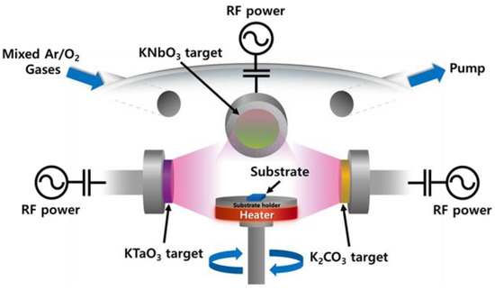
Figure 1.
Schematic diagram of the home-built off-axis sputtering system equipped with 3 sputtering guns and RF power sources.

Table 1.
Deposition parameters of RF magnetron co-sputtering for KTN thin films.
2.2. Characterization
The crystal structure and composition of the films were analyzed using a high-resolution X-ray diffractometer (HRXRD, Rigaku, ATX-G) with monochromated CuKα1 radiation (λ = 0.15406 nm) and field emission electron probe microanalyzer (EPMA, JEOL, JXA-8500F), respectively. Surface morphologies and film thicknesses were examined by field emission scanning electron microscopy (FE-SEM, FEI, Inspect-F) with acceleration voltages, working distance, and magnifications of 10–20 kV, 10 mm, and ×10–100 K, respectively. Raman spectra were recorded at room temperature using a micro-Raman system (UniRAM, UniNanotech, Yongin-si, Korea) to identify the phase of the KTN films. Variable temperature Raman measurements were then performed to investigate the phase transition behavior of KTN films. In addition, a spectroscopic ellipsometer (SE, Nano-View, MG-1000) was used to obtain optical constants (n and k) of KTN films in the range of 350–850 nm at an incident angle of 70°. Subsequently, the SE data were fitted using a Lorentz oscillator model in the Ellyreg 1.0 software (Nano-View). The reliability of the fitting was verified by the comparison between the fitted results and the values reported in the literature.
3. Results and Discussion
As mentioned previously in the experimental section, the x value in the KTN thin films was controlled by RF powers applied to KT and KN targets. To deposit KTN thin films with x = 0.53, the same RF power was applied to both KT and KN targets. The resulting composition was verified by EPMA analysis, which suggests that the value of x can be controlled through RF powers applied to KT and KN targets. The amount of K in KTN thin films, expressed as K/(Ta + Nb) and analyzed using EPMA, was almost the same (0.91 ± 0.04) in all KTN films, except for KTN-01, which was deposited with much higher RF powers applied to KN and KT targets (Table 1). We speculate that the negligible difference arises from the small difference in the RF powers (30 W vs. 40 W) applied to the KC target. Despite the insignificant change in the amount of K, XRD results clearly reveal the effect of excess K supply on the crystal quality of KTN films.
Figure 2 shows the HRXRD patterns of KTN thin films grown on LAO (100) substrates depending on the RF powers applied to each target. As can be seen in Figure 2, all KTN films were grown with strong (100) preferential orientation of the ABO3 perovskite structure. However, in the case of KTN-01 thin film grown with RF powers of 100, 100, and 30 W for KT, KN, and KC targets, respectively, peaks associated with the pyrochlore phase were also observed in addition to the perovskite (110) reflection. Considering the large film thickness of ~1 μm resulting from high RF power of 100 W applied to both KT and KN targets, we posit that the appearance of the perovskite (110) reflection was caused by a relaxation of internal stress induced by lattice mismatch (~5.5%) between KTN (a = 3.9978 Å, JCPDS 04-020-6631, x = 0.45) and LAO (a = 3.789 Å) [20]. We note that the JCPDS card does not exist for x = 0.53. However, based on the JCPDS cards for x = 0.35 and 0.45, changes in the lattice constant are only ~0.1%. Thus, we have assumed that the lattice constant for x = 0.53 will also be comparable to these values. The two peaks at 14.5° and 29.2° could be indexed as (111) and (222) of the pyrochlore phase [JCPDS 00-052-0155]. While we were not able to identify the origin of the peak at 11.2°, we presume this peak to be associated with the K-deficient phase. The signatures from perovskite (110) and pyrochlore (111)/(222) almost completely disappeared when the RF power applied to both KT and KN targets was reduced to 50 W in KTN-02. The reduction in the RF power from 100 to 50 W not only causes a decrease in the growth rate, reducing film thickness from ~1000 to 275 nm, but also naturally induces a relative increase of excess K supply, resulting in the disappearance of the unwanted phases. However, the hypothesized signature of K-deficiency at 11.2° still persisted even after the RF power applied to KT and KN targets was further reduced to 40 W (KTN-03). This peak ultimately disappeared when the RF power applied to the KC target was increased from 30 to 40 W, while maintaining the RF power applied to KT and KN targets at 40 W. The observed trend indicates that this peak is indeed associated with the K-deficient phase, and thus suggests that the control of the growth rate and excess supply of K are critical factors in achieving high-quality KTN films without the formation of undesired phases or orientations.
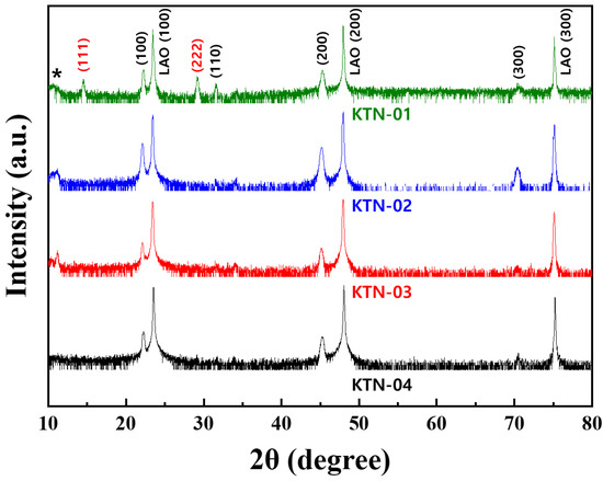
Figure 2.
HRXRD patterns of KTN thin films deposited on LaAlO3 substrate for 3 h depending on the RF power applied to targets. Black and red indices denote planes associated with perovskite and pyrochlore phases, respectively. Asterisk denotes unidentified peak which we presume to be a signature of the K-deficient phase.
Figure 3 shows HRXRD patterns of KTN thin films grown on LAO (100) and STO (100) single crystal substrates with two different deposition times of 3 and 6 h with 40 W of RF power applied to all targets. Under these conditions, perovskite KTN thin films with (100) preferred orientation were obtained on both LAO (100) and STO (100) substrates, as was the case for KTN-04. Based on the relative XRD peak intensities of the films and the substrates in Figure 3, KTN thin film on STO exhibits higher crystallinity to that deposited on LAO. The observed difference can be explained by the smaller lattice mismatch between KTN and STO. The lattice constant of STO is 3.905 Å [21] and, thus, the lattice mismatch between STO and KTN is about 2.4%. This is roughly ~43% of the mismatch (5.5%) expected between LAO and KTN, which makes the STO substrate more favorable for growing high-quality KTN thin films. The HRXRD patterns of thicker KTN films grown on these substrates (Figure 3) corroborate such findings. As can be seen in Figure 3, (110) the signature of perovskite KTN appeared in the thick (6 h) KTN film on LAO, which was absent in the thick (6 h) KTN film on STO. As the film thickness exceeds the critical thickness, the influence of the substrate’s crystal structure on the film is reduced, which results in randomly oriented growth from the initial preferentially oriented growth. It should be considered that the thickness at which randomly oriented growth initiates is dependent on the degree of lattice mismatch between the substrate and the thin film, and the greater the degree of lattice mismatch, the smaller the onset thickness. Upon initiation of the randomly oriented growth, the crystal plane with the lowest surface energy will start to nucleate first. Based on the XRD results, it is thought that the (110) orientation of perovskite KTN, which shows the strongest intensity in the JCPDS card (04-020-6631), corresponds to this plane.
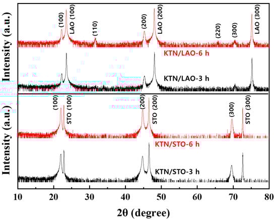
Figure 3.
HRXRD patterns of KTN thin films deposited on LaAlO3 and SrTiO3 substrates for 3 and 6 h.
Figure 4 shows surface and cross-sectional FESEM images of the KTN thin films grown on LAO substrates with various RF power combinations. The results will be discussed mainly in the context of two important parameters: (i) the absolute RF power of KT/KN targets and (ii) the RF power ratio of the targets (KC:KT/KN). We observe that decreasing absolute the RF power applied to both KT and KN targets improves the overall roughness and thickness uniformity. As can be seen in Figure 4, KTN-01 deposited at a growth rate of 5.56 nm/min exhibits a highly rough surface with large thickness non-uniformity. Considering the high RF powers applied to both KT and KN targets (100 W), such features are unsurprising as high deposition rates (i.e., high RF powers) generally give rise to rough surfaces. As expected, upon a significant decrease in the RF power from 100 to 50 W and, thus, the growth rate (1.53 nm/min), a drastic improvement in the roughness and thickness uniformity was observed (KTN-02). With an additional decrease in the RF power to 40 W, further improvements in the roughness and thickness uniformity were achieved despite the small decrease in the growth rate to 1.17 nm/min (KTN-03). KTN-03 and KTN-04 samples prepared using the same RF powers applied to KT and KN targets do not exhibit discrete changes in the roughness or thickness uniformity, which is consistent with the explanations provided above on the growth rate.
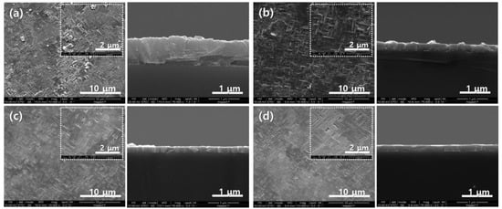
Figure 4.
Surface morphologies and cross-sectional images of KTN thin films deposited on LaAlO3 substrate for 3 h as a function of RF power applied to targets. The growth rates were obtained from cross-sectional images: (a) KTN-01, 5.56 nm/min (b) KTN-02, 1.53 nm/min (c) KTN-03, 1.17 nm/min, and (d) KTN-04, 1.17 nm/min.
On the other hand, the RF power ratio of KC to KT/KN has a significant impact on the surface microstructure and orientation of KTN films. In KTN-01 with a low RF power ratio of 0.3, a mixture of elongated rectangular shaped grains and needle-like grains are observed. We believe that the elongated rectangular shaped grains correspond to the (100) oriented perovskite phase, whereas the needle-like grains correspond to the (111) oriented pyrochlore phase. This is in good agreement with the XRD results, which showed the formation of the pyrochlore phase under K-deficient conditions. When the RF power ratio was doubled to 0.6 in KTN-02, needle-like grains associated with the pyrochlore phase were no longer present, which suggests that the power ratio plays a crucial role in the formation of the secondary or mixed phases in KTN thin films. Upon further increase in the power ratio (KTN-03), larger and denser grains were observed, implying improved crystallinity, which is also consistent with the XRD results. Owing to such a small increase in the RF power ratio in the KTN-04 sample, we did not observe a noticeable change in the surface microstructure. As such, KTN thin films grown on STO substrates using the conditions for KTN-04 and their microstructures are shown in Figure 5. Here, the surface morphology was nearly featureless in contrast to those deposited on LAO substrates. The improved surface morphology on STO (vs. LAO) originates not only from the smaller lattice mismatch between KTN and STO, but also because STO possesses a low density of planar defects unlike LAO, which exhibits a high density of twin defects. For these reasons, KTN films on STO substrate exhibit negligible changes in the microstructure even when the film thickness was nearly doubled, as shown in the HRXRD results. These results prove that careful control of the absolute RF power of KT/KN and the RF power ratio allows for tailoring of the extrinsic properties (e.g., surface morphology, microstructure, thickness uniformity, phase orientation, etc.) of KTN thin films.
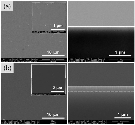
Figure 5.
Surface morphologies and cross-sectional images of KTN thin films deposited on SrTiO3 substrate for (a) 3 h and (b) 6 h.
We also performed Raman spectroscopy and spectroscopic ellipsometry on KTN-04 samples. For Raman spectroscopy, LAO substrates were used as the Raman modes of STO substrate overlap with those of KTN [22]. For spectroscopic ellipsometry (SE), on the other hand, STO substrates were used due to the inconsistent twin structure of the LAO substrates, which complicates the analysis.
Figure 6 shows temperature-dependent Raman spectra of KTN-04 on LAO substrate from room temperature (RT) to ~580 K. As shown in the figure, Fano resonance [23] associated with the ferroelectric phase was clearly observed around 190 cm−1 at RT [6,23]. In KTN, the broad Nb-O vibrations are present as a continuous background and the Ta-O vibrations exist as sharp, discrete states [23]. With increasing temperature, the Fano resonance disappeared around 403 K, as can be seen in the inset of Figure 6, indicating a ferroelectric to paraelectric phase transition. The transition temperature was slightly higher than the calculated value (~390 K) considering the composition (x = 0.53) of KTN-04 film [7]. We hypothesize that the shift in transition temperature is caused by substrate-induced interfacial strain from a lattice mismatch and/or difference in thermal expansion coefficients between KTN film and LAO substrate [6].
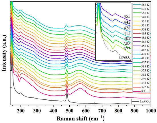
Figure 6.
Temperature-dependent Raman spectra of KTN thin film on LaAlO3 substrate.
The refractive index n and extinction coefficient k of the KTN-04 thin film grown on STO substrate are examined as a function of the wavelength between 350 and 850 nm. The complex refractive index (n* = n + ik) is an important property for optical materials, especially considering applications in optical switches, filters, modulators, and optoelectronic devices [24]. To obtain the refractive index and extinction coefficient, SE was performed. Ellipsometry measured the complex reflectance ratio between s- (rs) and p-polarization (rp) according to Equation (1), where the changes in the polarization of the incident beam were quantified by the amplitude ratio (ψ) and phase difference (Δ) [25]:
The interface between the KTN film and STO substrate has little effect on the simulation results and, thus, a sample stack consisting of Air/KTN/STO substrate was employed [26] for initial modeling. Finally, the following Lorentz oscillator dispersion relation was used to fit the experimental results to extract both the refractive index and extinction coefficient of the KTN thin film [27]:
where ε∞ is the real part of the dielectric function when E→∞, Ak is the strength expressed in eV, Bk is the central energy of the k-th oscillator, and Ck is the broadening in eV. The values extracted by fitting the experimental results in the wavelength range of 350~800 nm are shown in Table 2.
Table 2.
The fitted constants obtained from the Lorentz oscillator model.
As can be seen in Figure 7, the n and k decreases with the increasing wavelength, exhibiting an ordinary dispersion behavior. This is a generally observed dispersion behavior in transparent dielectric materials, including PbTiO3, BaZrTiO3, and BaTiO3. It is well known that the ABO3 structure consists of a BO6 oxygen octahedron framework, which is closely related to the wavelength-dependent refractive dispersion [2]. The large extinction coefficient in the high energy region can be attributed to the absorption band of KTN near 370 nm [2]. As the wavelength increases above 400 nm, the extinction coefficient dramatically reduces and approaches zero. Such small extinction coefficients below 0.01 suggest good transparency of the KTN film, allowing for the transmission of incident light without decay or damping in the spectral range of λ > 400 nm, which is an essential feature for applications, such as optical switches and modulators.
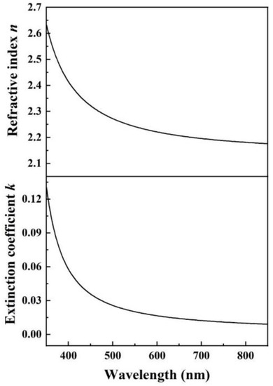
Figure 7.
Refractive index n and extinction coefficient k of KTN thin film on SrTiO3 substrate as a function of wavelength.
4. Conclusions
Ferroelectric perovskite KTN thin films with x = 0.53 were grown on LAO and STO single crystal substrates by using RF magnetron co-sputtering of KT, KN, and KC targets. The ratio of Ta/Nb in KTN thin films was mainly controlled by the RF powers applied to KT and KN targets, while compensation of K was achieved by the RF power applied to the KC target. With an RF power of 40 W applied to all three targets, the growth of (100) preferentially oriented perovskite KTN thin films on LAO (100) and STO (100) substrates was achieved. Temperature-dependent Raman spectra revealed that these KTN films exhibit a ferroelectric phase at RT and the phase transition from ferroelectric to paraelectric phase occurs at ~403 K. The n and k values of these KTN films obtained from SE were similar to those reported for single KTN crystals with similar compositions. Consequently, the results indicate that RF magnetron co-sputtering provides a simple way to grow high-quality KTN thin films. Further optimization of co-sputtering conditions is now in progress to deposit KTN films on various single crystal substrates, such as MgO and sapphire, which are relevant for device applications.
Author Contributions
Conceptualization, Y.-H.K.; investigation, G.-H.K. and K.C.J.; formal analysis, J.K. (Jongbum Kim) and J.K. (JoonHyun Kang); methodology, J.K. (JoonHyun Kang) and Y.-H.K.; writing—original draft, G.-H.K.; writing—review and editing, I.S.K. and Y.-H.K. All authors have read and agreed to the published version of the manuscript.
Funding
This work was funded by the Korea Institute of Science and Technology (Grant No. 2E31781).
Institutional Review Board Statement
Not applicable.
Informed Consent Statement
Not applicable.
Data Availability Statement
All data generated or analyzed during this study are included in this published article.
Conflicts of Interest
The authors declare no conflict of interest.
References
- Geng, W.; Qiao, X.; Zhao, C.; Zheng, D.; Li, Y.; Zhang, L.; Bi, K.; Yang, Y.; Sun, Y.; Chou, X. Temperature dependence of ferroelectric property and leakage mechanism in Mn-doped Pb(Zr0.3Ti0.7)O3 films. Ceram. Int. 2021, 47, 24047–24052. [Google Scholar] [CrossRef]
- Yang, W.; Zhou, Z.; Yang, B.; Jiang, Y.; Tian, H.; Gong, D.; Sun, H.; Chen, W. Structure and refractive index dispersive behavior of potassium niobate tantalate films prepared by pulsed laser deposition. Appl. Surf. Sci. 2011, 257, 7221–7225. [Google Scholar] [CrossRef]
- Imai, T.; Sasaura, M.; Nakamura, K.; Fujiura, K. Crystal growth and electro-optic properties of KTa1-xNbxO3. NTT Tech. Rev 2007, 5, 1–8. [Google Scholar]
- Zheng, X.; Zhao, H.; Wang, X.; Liu, B.; Yu, J.; Zhao, X. Phase evolution and dielectric/ferroelectric properties of KTa0.67Nb0.33O3 single crystal. Ceram. Int. 2015, 41, S197–S201. [Google Scholar] [CrossRef]
- Triebwasser, S. Study of Ferroelectric Transitions of Solid-Solution Single Crystals of KNbO3-KTaO3. Phys. Rev. 1959, 114, 63–70. [Google Scholar] [CrossRef]
- Bartasyte, A.; Kreisel, J.; Peng, W.; Guilloux-Viry, M. Temperature-dependent Raman scattering of KTa1−xNbxO3 thin films. Appl. Phys. Lett. 2010, 96, 262903. [Google Scholar] [CrossRef]
- Rousseau, A.; Guilloux-Viry, M.; Dogheche, E.; Bensalah, M.; Remiens, D. Growth and optical properties of KTa1−xNbxO3 thin films grown by pulsed laser deposition on MgO substrates. J. Appl. Phys. 2007, 102, 093106. [Google Scholar] [CrossRef]
- Peng, W.; Guilloux-Viry, M.; Députier, S.; Bouquet, V.; Simon, Q.; Perrin, A.; Dauscher, A.; Weber, S. Structural improvement of PLD grown KTa0.65Nb0.35O3 films by the use of KNbO3 seed layers. Appl. Surf. Sci. 2007, 254, 1298–1302. [Google Scholar] [CrossRef]
- Tunaboylu, B.; Sashital, S.R.; Harvey, P.; Esener, S.C.; Bhalla, A. Synthesis and properties of KTN films by sol-gel deposition and RF-magnetron sputtering. Ferroelectr. Lett. Sect. 2001, 28, 75–84. [Google Scholar] [CrossRef]
- Nazeri, A. Crystallization of sol-gel deposited potassium-tantalate-niobate thin films on platinum. Appl. Phys. Lett. 1994, 65, 295–297. [Google Scholar] [CrossRef]
- Buršík, J.; Železný, V.; Vaněk, P. Preparation of potassium tantalate niobate thin films by chemical solution deposition and their characterization. J. Eur. Ceram. Soc. 2005, 25, 2151–2154. [Google Scholar] [CrossRef]
- Glinšek, S.; Malič, B.; Kutnjak, Z.; Wang, H.; Krupka, J.; Kosec, M. Dielectric properties of KTa0.6Nb0.4O3 thin films on alumina substrates prepared by chemical solution deposition. Appl. Phys. Lett. 2009, 94, 172905. [Google Scholar] [CrossRef]
- Onoe, A.; Yoshida, A.; Chikuma, K. Epitaxial growth of orientation-controlled KNbO3 crystal films on MgO using KTaxNb1−xO3 intermediate layer by metalorganic chemical vapor deposition. Appl. Phys. Lett. 2001, 78, 49–51. [Google Scholar] [CrossRef]
- Fernandez, F.E.; Pumarol, M.; Marrero, P.; Rodriguez, E.; Mourad, H.A. Study of KTN Thin Films of Variable Composition grown by Pulsed Laser Deposition. MRS Proceedings 1997, 493, 365. [Google Scholar] [CrossRef]
- Jia, Y.; Winkler, M.; Cheng, C.; Chen, F.; Kirste, L.; Cimalla, V.; Žukauskaitė, A.; Szabados, J.; Breunig, I.; Buse, K. Pulsed laser deposition of ferroelectric potassium tantalate-niobate optical waveguiding thin films. Opt. Mater. Express 2018, 8, 541–548. [Google Scholar] [CrossRef]
- Laur, V.; Rousseau, A.; Tanne, G.; Laurent, P.; Deputier, S.; Guilloux-Viry, M.; Huret, F. KTa0.6Nb0.4O3 ferroelectric thin film behavior at microwave frequencies for tunable applications. IEEE Trans. Ultrason. Ferroelectr. Freq. Control 2006, 53, 2280–2286. [Google Scholar] [CrossRef]
- Savvinov, A.A.; Siny, I.G.; Katiyar, R.S.; Pumarol, M.; Mourad, H.A.; Fernandez, F.E. Investigations on KTN thin films by XRD, XPS and micro raman spectroscopy. Integr. Ferroelectr. 2000, 29, 13–20. [Google Scholar] [CrossRef]
- Yilmaz, S.; Venkatesan, T.; Gerhard-Multhaupt, R. Pulsed laser deposition of stoichiometric potassium-tantalate-niobate films from segmented evaporation targets. Appl. Phys. Lett. 1991, 58, 2479–2481. [Google Scholar] [CrossRef]
- Eom, C.B.; Sun, J.Z.; Yamamoto, K.; Marshall, A.F.; Luther, K.E.; Geballe, T.H.; Laderman, S.S. In situ grown YBa2Cu3O7−d thin films from single-target magnetron sputtering. Appl. Phys. Lett. 1989, 55, 595–597. [Google Scholar] [CrossRef]
- Chen, C.; Fang, L.; Zhang, J.; Zhao, G.; Ren, W. Thickness Control of the Spin-Polarized Two-Dimensional Electron Gas in LaAlO3/BaTiO3 Superlattices. Sci. Rep. 2018, 8, 467. [Google Scholar] [CrossRef]
- Janotti, A.; Jalan, B.; Stemmer, S.; Van de Walle, C.G. Effects of doping on the lattice parameter of SrTiO3. Appl. Phys. Lett. 2012, 100, 262104. [Google Scholar] [CrossRef]
- Gasparov, L.; Jegorel, T.; Loetgering, L.; Middey, S.; Chakhalian, J. Thin film substrates from the Raman spectroscopy point of view. J. Raman Spectrosc. 2014, 45, 465–469. [Google Scholar] [CrossRef]
- Wu, Y.; Liang, F.; Wang, X.; Wang, J.; Yu, H.; Zhang, H. Temperature dependent Raman spectroscopic study of Fano resonance in perovskite ferroelectric KTa1-xNbxO3 single crystal. Opt. Mater. Express 2022, 12, 247–255. [Google Scholar] [CrossRef]
- Hassanien, A.S.; Akl, A.A. Optical characterizations and refractive index dispersion parameters of annealed TiO2 thin films synthesized by RF-sputtering technique at different flow rates of the reactive oxygen gas. Phys. B Condens. Matter 2020, 576, 411718. [Google Scholar] [CrossRef]
- Azzam, R.M.; Bashara, N.M.; Ballard, S.S. Ellipsometry and Polarized Light; North-Holland: Amsterdam, The Netherlands, 1977. [Google Scholar]
- Hu, J.; Wang, J.; Wei, Y.; Wu, Q.; Zhang, F.; Xu, Q. Effect of film growth thickness on the refractive index and crystallization of HfO2 film. Ceram. Int. 2021, 47, 33751–33757. [Google Scholar] [CrossRef]
- Jellison, G.E. Data analysis for spectroscopic ellipsometry. Thin Solid Films 1993, 234, 416–422. [Google Scholar] [CrossRef]


Publisher’s Note: MDPI stays neutral with regard to jurisdictional claims in published maps and institutional affiliations. |
© 2022 by the authors. Licensee MDPI, Basel, Switzerland. This article is an open access article distributed under the terms and conditions of the Creative Commons Attribution (CC BY) license (https://creativecommons.org/licenses/by/4.0/).