
Photoresist Microlens Arrays Fabricated by Nanoimprint Technique to Improve the Photoelectric Conversion Efficiency of Solar Cells


1
College of Electronic and Optical Engineering & College of Microelectronics, Nanjing University of Posts and Telecommunications, Nanjing 210023, China
2
Peter Grunberg Research Center, Nanjing 210023, China
*
Authors to whom correspondence should be addressed.
Coatings 2022, 12(12), 1812; https://doi.org/10.3390/coatings12121812
Submission received: 19 October 2022
/
Revised: 15 November 2022
/
Accepted: 23 November 2022
/
Published: 24 November 2022
(This article belongs to the Special Issue Advanced Functional Nanostructured Films and Coatings for Energy Applications)
Abstract
:Silicon solar cells have the advantages of non-toxicity, reliability, low price, and stability. Microlens arrays (MLAs) are widely used in solar cells to improve photoelectrical conversion efficiency (PCE). In this research, different MLAs mold was designed by a method of thermal reflow. Then the photoresist film MLAs structure was replicated on the surface of silicon solar cells through UV nanoimprint technology. The optical transmission and surface morphology of these photoresist films were respectively measured by using a UV spectrometer and an atomic force microscope. The surface morphology and imaging capabilities of photoresist film MLAs were respectively measured by using a scanning electron microscope and optical microscope. Finally, the photovoltaic performance of the silicon solar cell with the photoresist film MLAs was investigated, and the PCE value of the silicon solar cell improved from 11.53% for the sample without MLAs to 13.19% for the sample with the square MLAs and the PCE improvement is about 14.40%. All these results above show that the photoresist film MLAs can significantly improve the efficiency of silicon solar cells and have great application potential in the field of solar cells.
1. Introduction
Solar energy, a non-polluting renewable green energy, has received extensive attention [1]. Many kinds of solar cells have been designed, including silicon solar cells [2], allium arsenide cells [3], perovskite cells [4,5,6], dye-sensitized solar cells [7], and so on. Moreover, silicon solar cells have already owned the highest market share in recent years owing to their non-toxicity, low price, stability, high conversion efficiency, reliability, and mature manufacturing technology [8,9,10].
There are two processes in the silicon solar cells that generate photoelectrical power. The absorption of photons causes the excitation of electron-hole pairs and the transport and separation of electron-hole pairs to external electrodes. Two main factors influence the efficiency of these silicon solar cells. One factor is the reflectance of the surface of the silicon solar cell, which affects the total amount of light absorption, and another factor is the collection of the photo-generated carriers and the loss of photo-generated carrier recombination.
In order to effectively collect photo-generated carriers and suppress the recombination loss of photo-generated carriers, many high-efficiency silicon solar cells were produced, such as the passivated emitter rear cell (PERC), the heterojunction solar cells with interdigitated back contacts (HBC), and the interdigitated back contact cell (IBC) [11]. However, these solar cells involve complicated technologies and may not be suitable for extensive production. Micro/nanostructures are generally used to decrease the reflectivity of the surface of silicon solar cells. These structures are usually used on the surface of silicon solar cells by etching technology or UV nanoimprint technology. These methods are relatively simple to operate and are suitable for extensive applications in solar cells.
Many kinds of methods can fabricate micro/nanostructures, such as microspheres self-assembly, partial-filling hot embossing technique, femtosecond laser direct writing, and the thermal reflow method. Compared with other methods, the advantages of nanoimprint technique has the advantages of simple operation, high feasibility, and low price. Many kinds of microstructures, such as micro/nanocones [12], nanowires [13,14], nanospheres [15], inverted pyramids [16], and nanopillars [17], have been proposed to reduce surface reflection to improve the PCE of the solar cells. Microlens arrays (MLAs) are used in solar cells to improve photoelectric conversion efficiency due to their excellent optical properties. For example, Gao et al. fabricated a Moth-eye nanostructure, which increased the reflectivity by 46.6% and improved the PCE of ultra-thin c-Si solar cells by 42.3% [18]. Huang et al. fabricated double-layer nano-pyramid arrays on thin-film solar cells [19]. The integrated absorption and PCE of the solar cell were increased by 45.31% and 15.77%. Osama et al. fabricated the 2D non-close-packed nanopore arrays on the perovskite layer, and the devices achieved a champion PCE of 11.64% [20].
In this work, we fabricated original MLAs molds of three different shapes using the thermal reflow method [21]. Photoresist film MLAs were replicated from the original MLAs mold by using UV nanoimprinting and applied on silicon solar cells [22]. The surface topography and optical properties of the photoresist film were investigated. The photoresist film MLAs can reduce the reflectivity of the substrate and have a great application value in the field of optics. Then the properties of current voltage, fill factor, and power of silicon solar cells with different shapes of photoresist film MLAs were measured, and it was found that the photoelectrical conversion efficiency (PCE) of the solar cells with square film MLAs has the maximum improvement of about 14.40%. Finally, the change in the conversion efficiency of solar cells under different incident angles of sunlight was studied.
2. Materials and Methods
2.1. The Design of MLAs Mask
The MLAs mask with three different microlens shapes was designed as shown in Figure 1. It can be easily found from Figure 1 that the circular and hexagonal MLAs have the regular hexagon arrangement, and the square MLAs have the square arrangement. D1, D2, and D3, respectively, are the diameter lengths of the MLAs. d1, d2, and d3 represent the spacing between adjacent MLAs. The filling factors of these MLAs have been calculated as 80.11%, 89.23%, and 86.58%, respectively, for the circular, square, and hexagonal MLAs. The detailed parameters of the MLAs, including the diameter and spacing, can be found in Table 1.
2.2. Fabrication Process of Photoresist Film MLAs on Silicon Solar Cells
The process of preparing photoresist film MLAs on silicon solar cells is demonstrated in Figure 2. The whole process concludes in two steps. First, a photoresist thermal reflow method is used to prepare the original MLAs mold, as shown in Figure 2A–D. Second, the photoresist film MLAs were fabricated on silicon solar cells using UV nanoimprint technology, as shown in Figure 2E–I.
2.3. Preparation of Original MLAs Mold
The original MLAs mold was fabricated by the thermal reflow method. This is shown in Figure 2A–D. First, the photoresist (AZ4620) was spin-coated on a circular substrate at a high speed of 2000 rpm for 30 s. This film was then prebaked at 100 °C for 10 min so that the excess solvent from the photoresist could be removed. The Ge mask was placed under a 300 W UV high-pressure mercury lamp for the exposure of the photoresist film. The exposure time of UV light (365 nm) was 180 s. We dropped the sample in the developer (AZ300MIF) for 300 s; then, photoresist cylindrical islands were formed on the substrate. Then, we rinsed the sample with DI water. Finally, the sample was placed on the plate at 140 °C for 45 min for the photoresist thermal reflow process and finally obtained the original MLAs mold. It should be emphasized that the experimental conditions of the different structural MLAs molds are the same.
2.4. Fabrication of Photoresist Film MLAs on Silicon Solar Cells
Figure 2E–I show the fabrication of MLAs on silicon solar cells by UV nanoimprinting technology. PDMS monomer (Sylgard 184) was blended with the curing agent at a weight ratio of 10:1. Then, this mixture was poured slowly onto an original MLA mold. We placed the sample in a vacuum drying oven and heated it at 80 °C for 45 min. After the sample was cooled, the PDMS soft template was removed from the original MLA mold. Next, we used a spin coater to deposit a photoresist (NOA63) film on the surface of a silicon solar cell at a high spin coating speed of 2000 rpm for 60 s. The PDMS mold with the MLAs was pressed onto a photoresist film; then, this sample was exposed to ultraviolet light (365 nm) for 10 min under a xenon lamp (300 w), and the intensity of the light was 1200 mW/cm2. In the end, this PDMS mold with the MLAs was peeled off, and the photoresist film MLAs were prepared on the silicon solar cells. Silicon solar cells were purchased from Anyang Sunshine Science and Education Energy Co., Ltd. (Anyang, China).
2.5. Characterizations
The surface topography and roughness of the photoresist films were investigated with an atomic force microscope (AFM, Bruker Dimension Icon, Karlsruhe, Germany).
The optical transmittance of these photoresist films, which were fabricated on glass substrates, was characterized with a UV spectrometer (USA UNICO UV-2800A, Shanghai Bayu Co., Ltd., Shanghai, China). We measured the surface profile of the photoresist film MLA with a step profiler (Alpha-Step D-500 KLA, Shanghai, China). The surface topography of these photoresist film MLAs was measured by scanning electron microscopy (SEM, S-4800, Hitachi, Tokyo, Japan). These imaging capabilities of photoresist film MLAs were all investigated by an inverted optical microscope (Ti2-E, Nikon, Japan). The photovoltaic performance of the solar cells was investigated by a solar workstation (SAN-EI, Hitachi, Tokyo, Japan) at AM 1.5.
3. Results
3.1. Optical Properties of The Photoresist Films
In this work, the optical character of these photoresist films was investigated. Figure 3A demonstrates an AFM image of this photoresist film with an area of 10 μm × 10 μm. Furthermore, these films were fabricated on glass substrates at the high spinning speed of 2000 rpm for 60 s. Then these films were exposed to the UV light for 10 min. As can be observed from Figure 3A that the surface of this photoresist film was clean and smooth. Furthermore, the roughness Ra of this photoresist film is 2.51 nm. Figure 3B manifests the optical transmittance of this photoresist film, which was fabricated on a glass substrate. As can be observed from Figure 3B that this transmittance value of the film in the light region from 350 to 800 nm is higher than 95%, which has great application value in the field of photovoltaic cells.
3.2. The Optical Transmittance of Photoresist Film MLAs
Figure 4 shows the optical transmittance of the photoresist film MLAs with different shapes and deposited on glass substrates. It can be clearly observed that the photoresist film MLAs have a suitable light transmittance of about 90%. It has great application value in the field of photovoltaic cells.
3.3. The Surface Topography of Photoresist Film MLAs
The SEM images and surface profiles of the photoresist film MLAs are manifested in Figure 5. As can be observed clearly from Figure 5A–C, these photoresist film MLAs are on a smooth surface, the MLAs are tightly arranged, and there is no obvious damage. Figure 5D–F displays that the diameter of the circular microlens is about 16.50 μm, the side length of the hexagonal and square microlens, respectively, is 15.63 and 15.1 μm, and the heights are 3.20, 2.98, and 3.18 μm, respectively. There is some size difference between the photoresist film MLAs and the original mask, which is mainly caused by the thermal reflow and UV nanoimprint process.
3.4. Optical Imaging Capabilities of Photoresist Film MLAs
Optical imaging properties of the photoresist film MLAs were investigated by an inverted optical microscope system. Moreover, Figure 6 manifests (A) the schematic of the imaging system and the virtual images of (B) circular, (C) hexagonal, and (D) square photoresist film MLAs. It should be mentioned that the photoresist film MLAs were fabricated on glass substrates. The test procedure is as follows: the photoresist film MLAs were first put on the optical platform. Furthermore, a tin foil mask in the shape of the letter “T” was placed between the microscope light source and these photoresist film MLAs. A CCD camera can be applied to catch the light penetrating through this “T”-shaped mask and the photoresist film MLAs. Figure 5 manifests virtual images of the (B) circular, (C) hexagonal, and (D) square photoresist film MLAs, which show suitable imaging capabilities.
3.5. The Transport Mechanism of Sunlight on Silicon Solar Cells
The fabricated photoresist film MLAs are applied to silicon solar cells. Figure 7A,B show the photographs of the silicon solar cells (A) without the photoresist film MLAs and (B) with the photoresist film MLAs. The size of both solar cells is 2 cm × 2 cm. Figure 7C,D show the transmission principle of the light on the silicon solar cell device. As shown in Figure 7C, when the light is incident vertically on the bare solar cell device, it will return back to the original path. As shown in Figure 7D, if the light hits the surface of the solar cell device with the photoresist film MLAs vertically, there will be three kinds of reflection paths (I, II, III). Light I, II will be reflected and dissipated in the air, but light III will be absorbed by the silicon solar cells. The utilization of light energy will be improved.
3.6. Photovoltaic Properties of These Solar Cells
Photovoltaic properties of these silicon solar cells were characterized. Figure 8 shows (A) I-V curves and (B) P-V curves of the silicon solar cells with flat photoresist film and photoresist film MLAs compared with the original silicon solar cells without photoresist film MLAs. As can be observed from Figure 8A that the short-circuit current of the solar cell with a flat photoresist film has a small increase than that of an original solar cell. Moreover, this short-circuit current of the solar cell with the photoresist film MLAs has an obvious increase to that of an original solar cell. The properties of the solar cell with a flat photoresist film have a small increase than an original solar cell. Then the current of these silicon solar cells with photoresist film MLAs from 0 to 0.5 voltage is significantly larger than the original silicon solar cell. It can also be obtained from Figure 8B that the power of the silicon solar cells with the photoresist film MLAs is larger than that of the original silicon solar cell and the solar cell with a flat photoresist film within the voltage of 0.1–0.5 V. The current voltage, fill actor, current density, and photoelectric conversion efficiency of the original solar cell have been measured as 570.0 mV, 65.93%, 30.85 mA/cm2, and 11.53%. The maximum power (Pmax) value of the silicon solar cells with circular, hexagonal, and square MLAs is 49.24, 50.91, and 52.75 mW, respectively. Table 2 shows that the photoresist film MLAs increased the short-circuit current density Jsc by 6.74% for circular photoresist film MLAs, 6.35% for hexagonal photoresist film MLAs, and 7.39% for square photoresist film MLAs, and the open-circuit voltage Voc has minor changes. The fill factor of the silicon solar cells with the photoresist film MLAs has great improvement, especially the silicon solar cell with square MLAs, in which the value was increased from 65.93% to 70.25%. The PCE value for the silicon solar cells with circular, hexagonal, and square photoresist film MLAs can be calculated respectively as 12.31%, 12.73%, and 13.19%. The maximum PCE improvement of the silicon solar cell is improved from 11.53% for the sample without the microstructure to 13.19% for the sample with the square MLAs, and the PCE improvement is about 14.40%. This is probably because the square MLAs have the highest fill factor. The above results display that the photoresist film MLAs can improve the capability of silicon solar cells, especially the square MLAs.
Figure 9 shows the change in the photoelectric conversion efficiency of solar cells under different incident angles of sunlight. As the angle of incidence increases, the PCE of these silicon solar cells gradually decreases, while these solar cells with photoresist film MLAs exhibit superior solar power generation over a wide incident angle range of 0–60°. Moreover, the solar cell with a flat photoresist film also has a slight improvement to that of the original solar cell. This is because the photoresist film MLAs reduce the reflection and increase the incident light. The results show that the photoresist film MLAs can also improve the photoelectric conversion efficiency of solar cells under different incident angles of the sunlight and have strong adaptability.
4. Conclusions
Three types of photoresist film MLAs were successfully fabricated on silicon solar cells by UV nanoimprint technology. These prepared photoresist films have a smooth surface and a suitable optical transmittance of above 95% in the visible light range. The photoresist film MLAs also have a clear surface and suitable imaging properties. Moreover, the photovoltaic performance of these solar cells with photoresist film MLAs was investigated, including the current voltage, fill actor, current density, and photoelectric conversion efficiency. The results show that the photoresist film MLAs can improve the short-circuit current density, fill actor, resulting in considerable enhancement of PCE, and the silicon solar cells with square MLAs have the maximum PCE improvement of about 14.40%. These findings demonstrate the promising application of photoresist film MLAs in solar cell devices.
Author Contributions
Writing—review and editing, X.Z. (Xuehua Zhang); writing—original draft preparation, L.L.; data curation, X.Z. (Xinwen Zhang); project administration, X.Z. (Xuehua Zhang) and F.H. All authors have read and agreed to the published version of the manuscript.
Funding
National Natural Science Foundation of China (NSFC) (Grant Nos.: 61605086, 51602160, 61574080, 61274121).
Institutional Review Board Statement
Not applicable.
Informed Consent Statement
Not applicable.
Data Availability Statement
Not applicable.
Conflicts of Interest
The authors declare no conflict of interest.
References
- Hossain, M.K.; Gazi, A.R.; Md, A.A.; Mirza, H.K.R.; Mohammad, H.A.; Khan, M.I.; Shahadat, H.; Sapan, K.S.; Jalal, M.I.E.; El-Denglawey, A. Current Applications and Future Potential of Rare Earth Oxides in Sustainable Nuclear, Radiation, and Energy Devices: A Review. ACS Appl. Electron. Mater. 2022, 4, 3327–3353. [Google Scholar] [CrossRef]
- Zhong, S.; Shen, W. Quasi-omnidirectional crystalline silicon solar cells. J. Phys. D Appl. Phys. 2020, 53, 483001. [Google Scholar] [CrossRef]
- Obaid, S.; Lu, L. Highly Efficient microscale gallium arsenide solar cell arrays as optogenetic power options. IEEE Photonics J. 2019, 11, 8400108. [Google Scholar] [CrossRef]
- Yu, Y.; Zhang, F.; Yu, H. Self-healing perovskite solar cells. Sol. Energy 2020, 209, 408–414. [Google Scholar] [CrossRef]
- Wali, Q.; Iftikhar, F.J.; Khan, M.E.; Ullah, A.; Lqbal, Y.; Jose, R. Advances in stability of perovskite solar cells. Org. Electron. 2020, 78, 105590. [Google Scholar] [CrossRef]
- Bencherif, H.; Mwddour, F.; Elshorbagy, M.H.; Hossain, M.K.; Cuadrado, A.; Abdi, M.A.; Bendib, T.; Kouda, S.; Alda, J. Performance enhancement of (FAPbI3)1−x(MAPbBr3)x perovskite solar cell with an optimized design. Micro. Nanostruct. 2022, 171, 207403. [Google Scholar] [CrossRef]
- Javed, A.H.; Shahzad, N.; Khan, M.A.; Ayub, M.; Lqbal, N.; Hassan, M.; Hussain, N.; Rameel, M.I.; Shahzad, M.I. Effect of ZnO nanostructures on the performance of dye sensitized solar cells. Sol. Energy 2021, 230, 492–500. [Google Scholar] [CrossRef]
- Son, H.J.; Hong, K.K.; Ju, B.K.; Kim, S.H. Oxidation-resistant Cu-Based metallisation for Si solar cells. Energy Sci. Eng. 2022, 10, 1264–1271. [Google Scholar] [CrossRef]
- Lu, L.; Adel, N.; Wang, K.; Du, M.Y.; Liu, S.Z. Perovskite Quantum Dots in solar Cells. Adv. Sci. 2022, 9, 2104577. [Google Scholar] [CrossRef]
- Hsu, C.H.; Zhang, X.Y.; Zhao, M.J.; Lin, H.J.; Zhu, W.Z.; Lien, S.Y. Silicon Heterojunction Solar Cells with p-Type Silicon Carbon Window Layer. Crystals 2019, 9, 402. [Google Scholar] [CrossRef] [Green Version]
- Liu, J.J.; Yao, Y.; Xiao, S.Q.; Gu, X.F. Review of status developments of high-Efficiency crystalline silicon solar cells. J. Phys. D Appl. Phys. 2018, 51, 123001. [Google Scholar] [CrossRef]
- Yang, D.; Zhang, T.R.; Wang, C.B.; Yu, T.T.; Wang, J.; Xu, Z.P. Enhanced electro-Optical properties of TiO2 Nanocone Arrays for ultrathin GaAs Solar cells. Opt. Commun. 2019, 452, 281–285. [Google Scholar] [CrossRef]
- Chen, W.H.; Cabarrocas, P.R.I. Rational design of nanowire solar cells: From single nanowire to nanowire arrays. Nanotechnology 2019, 30, 194002. [Google Scholar] [CrossRef]
- Adibzadeh, F.; Olyaee, S. Nanostructure back reflector for enhancing the performance of InP nanowire array solar cells. Opt. Quant. Electron. 2022, 54, 303. [Google Scholar] [CrossRef]
- Wei, P.K.; Hao, Z.W.; Yang, Y.; Liu, L. Hollow NiSe2 nanospheres grown on graphene with unconventional dual-Vacancies in dye-Sensitized solar cells. Appl. Surf. Sci. 2021, 553, 149567. [Google Scholar] [CrossRef]
- Tang, H.B.; Liu, Y.P.; Chen, Q.S.; Wang, Y.; Chen, W.; Wu, J.T.; Zhao, Y.; Du, X.L. Optical Design of Inverted Pyramid Textured PERC Solar Cells. ACS Appl. Electron. Mater. 2019, 1, 2684–2691. [Google Scholar] [CrossRef]
- Sun, P.; Qu, G.P.; Hu, Q.K.; Ma, Y.C.; Liu, H.S.; Xu, Z.X.; Huang, Z.F. Highly Efficient Large-Area Flexible Perovskite Solar Cells Containing Tin Oxide Vertical Nanopillars without Oxygen Vacancies. ACS Appl. Energ. Mater. 2022, 5, 3568–3577. [Google Scholar] [CrossRef]
- Gao, Z.L.; Lin, G.L.; Chen, Y.C. Moth-eye nanostructure PDMS films for reducing reflection and retaining flexibility in ultra-thin c-Si solar cells. Sol. Energy 2020, 205, 275–281. [Google Scholar] [CrossRef]
- Huang, Z.S.; Wang, B. Thin-Film Solar Cells by Silicon-Based Nano-Pyramid Arrays. Adv. Theor. Simul. 2022, 5, 2100586. [Google Scholar] [CrossRef]
- Osama, M.A.; Amal, A.; Muhamad, Z.M.; Ben, F.S.; Qian, C.; Andrew, G.T.; Nigel, W.H.; Wang, X.L.; Patrick, H.; Janet, J.; et al. High efficiency semitransparent perovskite solar cells containing 2D nanopore arrays deposited in a single step. J. Mater. Chem. A 2022, 10, 10227–10241. [Google Scholar]
- Shi, J.; Huang, Y.S.; Peng, L.N.; Ni, Z.J.; Zhang, D.W. Grating/microlens arrays fabricated by hot-melting, self-Assembly and replication. Opt. Mater. 2020, 104, 109733. [Google Scholar] [CrossRef]
- Baek, S.; Kim, K.; Sung, Y.; Jung, P.; Ju, S.; Kim, W.; Kim, S.J.; Hong, S.H.; Lee, H. Solution-processable multi-color printing using UV nanoimprint lithography. Nanotechnology 2020, 31, 125301. [Google Scholar] [CrossRef] [PubMed]
Figure 1.
The arrangement diagram of the special-shaped microlens array mold. (A) the circular, (B) the hexagonal, and (C) the square MLAs.
Figure 1.
The arrangement diagram of the special-shaped microlens array mold. (A) the circular, (B) the hexagonal, and (C) the square MLAs.

Figure 2.
Flow chart of the manufacturing process of the photoresist film MLAs on silicon solar cells. (A) Spin coating photoresist film on this silicon substrate, (B) exposure of the photoresist film to the UV light with Ge mask, (C) thermal reflow, (D) original photoresist mold, (E) replicating PDMS mold, (F) peeling off this mold, (G) pressing a PDMS mold on this photoresist film, (H) exposing this sample for solidification, (I) obtained silicon solar cells with MLAs.
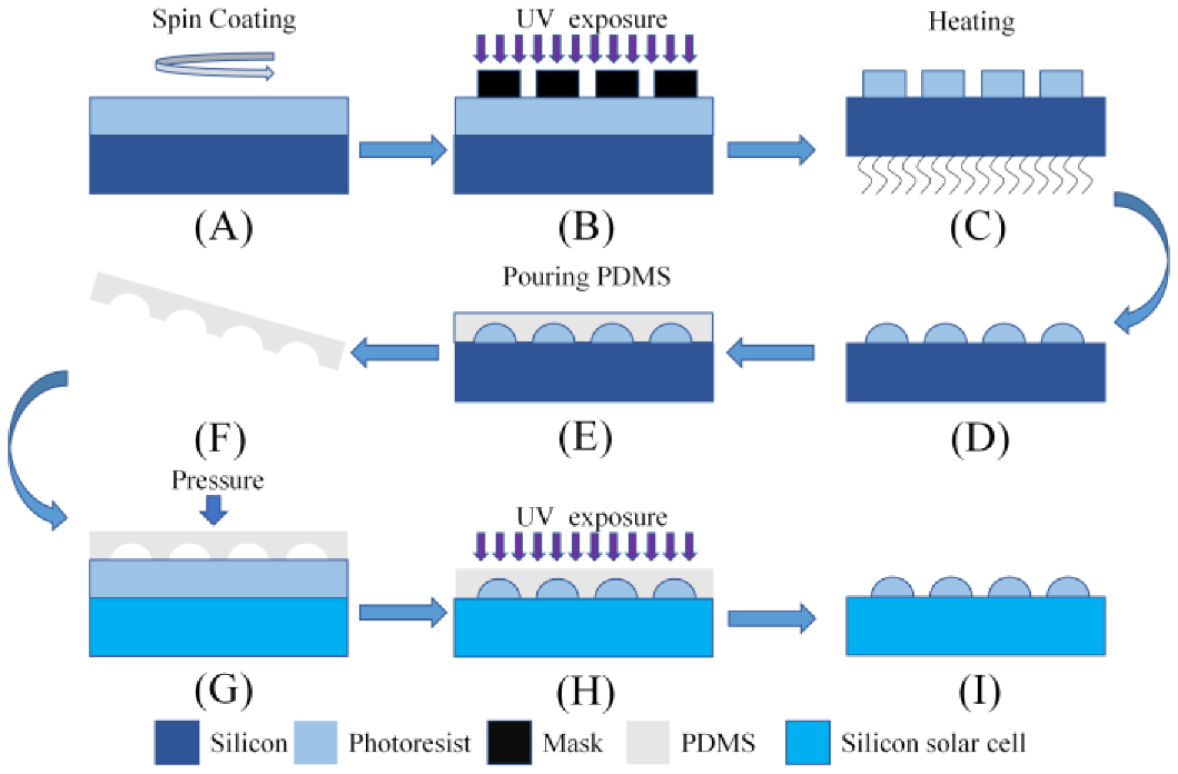
Figure 3.
(A) The AFM image and (B) the optical transmittance of the photoresist film.

Figure 4.
The optical transmittance of the photoresist film MLAs with different shapes and deposited on glass substrates.
Figure 4.
The optical transmittance of the photoresist film MLAs with different shapes and deposited on glass substrates.

Figure 5.
The SEM images and the surface profiles of (A,D) circular, (B,E) hexagonal, and (C,F) square photoresist film MLAs.
Figure 5.
The SEM images and the surface profiles of (A,D) circular, (B,E) hexagonal, and (C,F) square photoresist film MLAs.

Figure 6.
(A) The schematic of the imaging system and the virtual images of (B) circular, (C) hexagonal, and (D) square photoresist film MLAs.
Figure 6.
(A) The schematic of the imaging system and the virtual images of (B) circular, (C) hexagonal, and (D) square photoresist film MLAs.
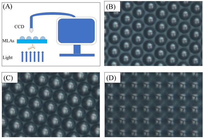
Figure 7.
Photographs of the solar cells (A) without photoresist film MLAs and (B) with the photoresist film MLAs, and the light path of the incident sunlight on (C) a bare solar cell and (D) a solar cell with the photoresist film MLAs and three kinds of reflected light (I, II, III).
Figure 7.
Photographs of the solar cells (A) without photoresist film MLAs and (B) with the photoresist film MLAs, and the light path of the incident sunlight on (C) a bare solar cell and (D) a solar cell with the photoresist film MLAs and three kinds of reflected light (I, II, III).
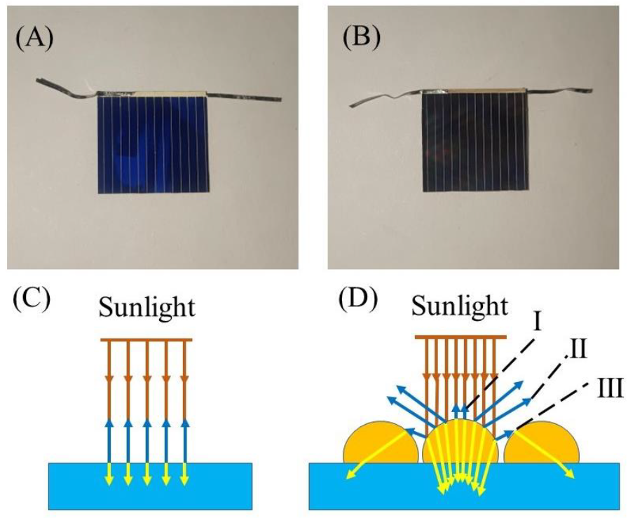
Figure 8.
(A) The I-V curves and (B) the P-V curves of silicon solar cells with flat film, circular, hexagonal, and square MLAs films compared with the silicon solar cells without photoresist film MLAs.
Figure 8.
(A) The I-V curves and (B) the P-V curves of silicon solar cells with flat film, circular, hexagonal, and square MLAs films compared with the silicon solar cells without photoresist film MLAs.
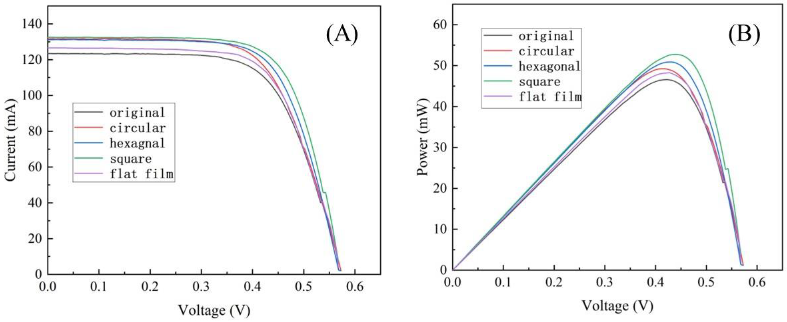
Figure 9.
Dependence of the solar cell PCEs on an incident angle with and without the photoresist film MLAs.
Figure 9.
Dependence of the solar cell PCEs on an incident angle with and without the photoresist film MLAs.


Table 1.
The detailed parameters of these MLAs mask.
| MLAs Shape | Diameter/Side Length (μm) | Space (μm) |
|---|---|---|
| Circular | 15 | 3 |
| Square | 15 | 3 |
| Hexagonal | 15 | 3 |
Table 2.
Specific parameters of silicon solar cells with different shapes of MLAs.
| Solar Cell with or without MLA | VOC (mV) | JSC (mA cm2) | Fill Actor (%) | Efficiency (%) |
|---|---|---|---|---|
| Reference | 570.0 | 30.85 | 65.93 | 11.53 |
| Circular | 574.5 | 32.93 | 65.08 | 12.31 |
| Hexagonal | 569.4 | 32.81 | 68.12 | 12.73 |
| Square | 566.6 | 33.13 | 70.25 | 13.19 |
| Flat film | 559.2 | 31.64 | 68.39 | 12.10 |
Publisher’s Note: MDPI stays neutral with regard to jurisdictional claims in published maps and institutional affiliations. |
© 2022 by the authors. Licensee MDPI, Basel, Switzerland. This article is an open access article distributed under the terms and conditions of the Creative Commons Attribution (CC BY) license (https://creativecommons.org/licenses/by/4.0/).
Share and Cite
MDPI and ACS Style
Zhang, X.; Lv, L.; Zhang, X.; Hu, F. Photoresist Microlens Arrays Fabricated by Nanoimprint Technique to Improve the Photoelectric Conversion Efficiency of Solar Cells. Coatings 2022, 12, 1812. https://doi.org/10.3390/coatings12121812
AMA Style
Zhang X, Lv L, Zhang X, Hu F. Photoresist Microlens Arrays Fabricated by Nanoimprint Technique to Improve the Photoelectric Conversion Efficiency of Solar Cells. Coatings. 2022; 12(12):1812. https://doi.org/10.3390/coatings12121812
Chicago/Turabian StyleZhang, Xuehua, Liangwei Lv, Xinwen Zhang, and Fangren Hu. 2022. "Photoresist Microlens Arrays Fabricated by Nanoimprint Technique to Improve the Photoelectric Conversion Efficiency of Solar Cells" Coatings 12, no. 12: 1812. https://doi.org/10.3390/coatings12121812
Note that from the first issue of 2016, this journal uses article numbers instead of page numbers. See further details here.