Article

Chemical Stability of Sputter Deposited Silver Thin Films

Department of Solid State Sciences, Ghent University, Krijgslaan 281 (S1), 9000 Gent, Belgium
Coatings 2022, 12(12), 1915; https://doi.org/10.3390/coatings12121915
Submission received: 10 November 2022 / Revised: 1 December 2022 / Accepted: 3 December 2022 / Published: 7 December 2022
(This article belongs to the Collection Feature Paper Collection in Thin Films)

Abstract

:
Silver films with a thickness below 50 nanometer were deposited on glass using DC magnetron sputtering. The chemical stability of the films was investigated by exposure of the film to a droplet of a HCl solution in a humid atmosphere. The affected area was monitored with a digital microscope. The affected area increases approximately linearly with time which points to a diffusive mechanism. The slope of the area versus time plot, or the diffusivity, was measured as a function of the acid concentration, the presence of an aluminum seed layer, and film thickness. The diffusivity scales linearly with the acid concentration. It is shown that the diffusivity for Al-seeded Ag films is much lower. The behavior as function of the film thickness is more complex as it shows a maximum.

1. Introduction

Thin silver films are used in a wide range of applications including antibacterial coatings [1] and different optical devices [2]. Silver thin films are deposited on a large scale as low emissivity (low-E) multilayers to improve the insulating properties of glazings [3,4]. Another application field of this type of multilayers is as transparent anode materials with low sheet resistance and high transparency which could replace the more expensive indium-based materials [5,6]. The multilayers consist of a stack of a metal layer sandwiched between two dielectric layers, such as aluminum-doped zinc oxide or TiO2 [7,8]. The three layer structure is often repeated, and one refers to the number of repetitions as a single, double, or triple low-E coating [9]. The multilayer acts as an optical filter to control the heat flux through architectural glazings. The filter must combine a high visual with a low infra-red transmittance. The optical properties of silver makes it the preferred metal used in low-E coatings. The fabrication of a thin silver film is challenging due its inherent three-dimensional growth on weakly-interacting substrates, such as most oxide films used in low-E coatings. Due to the tendency for 3D growth, continuous films can only be obtained at a relatively high mean film thicknesses. Therefore, strategies have been developed to overcome this problem. Silver can be alloyed with other elements [10,11,12,13,14]. Additionally, the use of gaseous surfactants has been reported [12,15,16]. The most common approach is however the deposition of metal seed layers prior to the silver deposition. The seed layer is typically a non-continuous thin film which affects the silver film growth. Prior to the deposition of the covering dielectric film, another often non-continuous layer, known as a blocking layer, protects the silver from reactive process conditions during the dielectric deposition. The optical properties of the low-E coatings are further optimized by material combinations, film thicknesses, and deposition conditions. The latter is currently performed in-line on large area coaters by magnetron sputtering [8,17]. The choice for the latter technique is mainly motivated by the good scalability of technique and the accurate control of the deposition rate.
Silver based low-E multilayers are vulnerable to humid air [18,19,20,21,22,23,24]. Therefore, the multilayer is deposited on the interior of the double glazing. Double glazings will normally fail due to internal fogging, when moisture appears between the panes. With an anticipated 20 year lifetime of double glazing, the long term chemical stability of silver thin film is an important feature. The protection of the multilayer in this way is however not always possible for the aforementioned applications.
Hence, the degradation mechanism of silver based low-E multilayers has been investigated in detail [19]. The proposed degradation model is based on a post-exposure study of degradation spots formed on ZnO/Ag/ZnO multilayers and Ag thin films exposed to a 95% relative humidity at room temperature over a saturated KCl solution. The spots contain a central particle which seems to act as an entry point of water, or result in a thinner film close to the particle due to geometrical shadowing effects during deposition. The degradation spot consists of agglomerated silver around the central particle. In the case of coated Ag layers, this agglomeration results in mechanical stress in the top dielectric, which can lead to delamination of the layer. Similar spots are observed during salt spray test on low-E coatings [14] or long-term exposure to high humidity conditions [25]. The role of the air humidity on the formation of “corrosion spots” has also been reported for other ultra-thin metal layers used in magnetic devices [26].
The origin of the silver agglomeration is less highlighted in the proposed degradation model [19]. A comparison with silver agglomeration due the thermal annealing is made with the minimization of internal and surface free energy and the important role of the surface diffusivity of Ag atoms as the driving force. The comparison seems to be plausible. Indeed, the agglomeration kinetics is based on hole growth [27] which can have multiple causes, such as grain boundary grooving, in the case of thermal annealing. As grain boundaries are more vulnerable to chemical attacks, grain boundary atoms will more easily and rapidly dissolve than atoms within the grains. This selected attack when the silver layer is exposed to humid air, could lead to holes exposing the substrate which will be followed by hole growth and an agglomerated silver film as a final result. This proposed mechanism agrees with the observations of Ross [19] as a chemical analysis of the islands uncovers no other elements than silver. Moreover, as silver is known to have a high surface diffusivity [28] it can be expected that especially thin silver films are quite sensitive to degradation through this mechanism as hole growth depends strongly on surface diffusion [29]. The silver aggregation can be further triggered by the interaction with chlorine atoms [30,31].
Although quite some knowledge has been gathered on the chemical stability of low-E coatings, and silver thin films in general, the kinetics of the degradation spot formation is, to the best of my knowledge, not studied in detail. In this study, the spot formation is induced on sputter deposited silver films by a local exposure to a diluted HCl droplet. The kinetics of the process is followed in situ. Image analysis permits a quantitative analysis of the spot size as function of the HCl concentration, film thickness and the presence of an aluminum seed layer.

2. Materials and Methods

A custom-made setup was built to follow the degradation spot formation (Figure 1). The sample is placed on a transparent glass plate. The glass plate is supported by the water cup. The water cup is a torus which can hold a tube. Distilled water is present between the tube interior and center of the water cup. The water cup is closed at the bottom by a transparent glass cover. The top of the tube is closed with a similar cover. As such, no water can evaporate and the humidity inside the tube will be close to 100%. A digital microscope (Dino-Lite, AM4115TL, 1.3 Megapixel) is placed on top of the upper glass cover. The opaque microscope support prevents light from entering from the top. The internal light source of the microscope is switched off. A bright white LED light source is placed below the set-up (not shown). The light source was cooled with a fan. The measuring procedure starts by placing the sample on the sample plate. A small alumina ring (diameter 2.75 mm, height 2 mm) is placed on the sample. The alumina ring ensures an equal contact area. Preliminary experiments showed that the droplet shape can change during the experiment and/or be different for films deposited under different conditions. A 3 μL droplet of diluted HCl solution is injected in the ring with a pipette. The tube is placed over the sample, and closed with the top glass cover and the microscope.
Prior to the measurement, the digital microscope settings are tuned to have an optimal image. After optimization, the auto-exposure setting was switched off together with the auto-white balance option. A constant exposure of the sample is necessary for further image analysis. Images at a 10-fold magnification were recorded at a fixed time interval using the camera software. The area of the degraded region was measured using ImageJ [32]. Calibration was performed using size of the alumina ring (approximately 120 pixels/mm). The blue channel of the image was converted into a binary image which can be automatically processed using the Analyze particles function of the ImageJ software.
Silver thin films were deposited on glass substrates that have been ultrasonic cleaned in a mixture of distilled water and ethanol (70% ethanol/30% water). The higher content of alcohol allows a faster drying of the substrates. A high vacuum chamber was pumped by a combination of a turbomolecular pump and a rotary pump. The base pressure during film deposition was lower than 4 × 10 4 Pa, as measured with a Penning pressure gauge. The argon pressure (0.5 Pa measured with a capacitance pressure gauge) was set by the introduction of argon at a rate of 36.8 standard cubic centimeter per minute (sccm) using a mass flow controller (MKS Instruments, Andover, MA, USA). A silver target (2 inch in diameter, 6 mm thick) was placed on a planar cylindrical magnetron powered by a Hüttinger 1500 DC power supply. The discharge current was fixed at 0.06 A which results in a discharge voltage of 369 V. The target-substrate distance equaled 10 cm. Another, identical magnetron, holding an aluminum target (3 mm thick), was placed directly opposite the silver magnetron. The target–substrate distance was 12 cm. The aluminum magnetron was used to deposit silver thin films with an aluminum seeding layer. First, the seed layer was deposited at the aforementioned pressure and discharge current. After sputter cleaning the silver target to avoid cross-contamination, the sample holder was flipped to expose the sample to the silver magnetron.
In the case of silver, the deposition rate was calculated from the deposition time and the film thickness as measured with X-ray reflectivity. At the aforementioned conditions, the deposition rate equals 0.340 ± 0.034 nm/s. In the case of aluminum, several thicker layers were deposited, and their thickness was measured with a stylus profilometer (Taylor Hobson, Talystep, Leicester, UK). The deposition rate was calculated based on the deposition time and the measured thickness. Based on this calibration the film thickness of the seed layer is approximately 0.5 nm (15 s deposition time at 0.06 A, and 306 V, at 0.5 Pa for a target-to-substrate distance of 12 cm).
The film resistivity was measured using a four probe (in-line) Van der Pauw method [33]. The resistivity measurement was performed directly after the film deposition. The films and the degradation spots were analyzed with by SEM-FEG (Fei Quanta, FEI, Hillsboro, OR, USA). X-ray diffraction (XRD) measurements in Bragg–Brentano configuration were performed with D8 Bruker (Billerica, MA, USA) set-up equipped with an Euler cradle. X-ray reflectivity (XRR) measurements were performed on a similar set-up. XRR and XRD measurements were performed on thin films deposited on RCA (Radio Corporation of America) cleaned silicon. Atomic force microscopy (AFM) measurements were performed on a Bruker Dimension Edge system.

3. Results

3.1. Image Analysis

Figure 2 shows a typical result of the degradation experiment. Figure 2a shows the evolution of the degradation spot as function of time. The images are taken at an interval of 45 s. The dark ring in the center of each image is a small alumina cylinder which holds the HCl solution droplet. The area of the affected region was measured (Figure 2c) using the ImageJ analysis software. The area increases, after a short initial delay, linearly with time. This points towards a diffusion-based mechanism. From the slope of a linear fit through the data, the associated diffusivity can be calculated. Subtraction of the initial recording from the other images permit the changes to be highlighted. Figure 2b shows the result for the last image taken. The degradation spot appears to be composed of three concentric rings.

3.2. Influence of HCl Concentration

A series of experiments was performed to investigate the influence of the HCl concentration on the diffusivity. The silver mean film thickness was fixed at approximately 20 nm (deposition time 60 s). For each concentration, a minimum of three films were deposited and consecutively tested. Six concentrations were tested in a concentration range between 0.25 wt% and 2.5 wt%. The diffusivity increases linearly with the HCl concentration. The slope equals 0.44656 mm2.s−1.wt%−1. The line goes through the origin ( r 2 = 0.9942 ) which indicates that at the timescale of the experiment (max. 10 min) the silver film is not affected by the humid atmosphere when no HCl is present.

3.3. Influence of Film Thickness

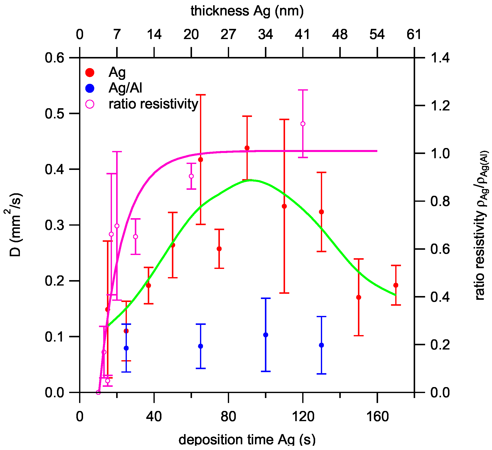
The influence of the silver film thickness on the diffusivity D was investigated by exposing the layers to a fixed concentration of 0.5%wt HCl solution droplets (see Figure 3). The error was calculated as the standard deviation of four deposition/exposure combinations. Despite the large error for some individual thicknesses, it is clear that the diffusivity increases initially with increasing thickness. At a film thickness of approximately 30 nm, the diffusivity maximizes and then decreases with increasing thickness.

3.4. Influence of the Seed Layer

The experiments discussed in previous section (Section 3.3) were repeated with a aluminum seed layer. The nominal thickness of the aluminum layer was fixed at 0.5 nm. The seed layer results in strong drop of diffusivity D. The diffusivity is significantly different from non-seeded layers with similar thicknesses, except for the thinnest film (deposition time 25 s, mean film thickness 8.5 nm). An ANOVA test shows that between the four studied thicknesses for the seeded layers no significant differences exist. Hence, there is no thickness dependency (blue markers Figure 3) and the average diffusivity equals 0.087 mm2·s−1 (±0.030, 95% confidence interval).

3.5. Film Characterization

3.5.1. As-Deposited Films

Samples of both seeded and non-seeded as-deposited films were analyzed with different techniques. The following paragraphs give an overview.
Seeded and non-seeded layers were analyzed using SEM. Seeded layers become continuous at a smaller nominal thickness. For example, a thin film with a nominal thickness of 6 nm without seed layer (image b, Figure 4) has a similar surface morphology as a seeded layer with a nominal thickness of 3 nm (image c, Figure 4).
The influence of the seed layer on the film resistivity measurements can be interpreted in the same way as above. It is possible to measure a film resistivity for seeded Ag films with a thickness as small as 3.3 nm while for the films deposited without seed layer the first measurement is only possible for a thickness of 4.4 nm. This indicates that the percolation threshold is reached at smaller mean thicknesses for the seeded layers. A plot of the R t film 2 vs. the film thickness, with R the film resistance and t film the film thickness (not shown), has a minimum which have been connected the continuity threshold [34]. A value of approximately 10 nm is obtained for Ag, while 6 nm is measured for Ag/Al thin films. Further, it can be observed from Figure 3 (right axis) that the same film resistivity is only measured at a film thickness at approximately 27 nm (80 s deposition).
Figure 5 gives an overview of the AFM analysis. The AFM roughness confirms the aforementioned observations. The thinnest films are very rough, especially for the non-seeded layer. After a strong drop, the roughness further (slightly) increases with increasing film thickness.
As demonstrated by the shown AFM images, for the two thickest films, the opposite is observed, i.e., the height density distribution of the seeded layers shows a stronger contribution of higher regions. The AFM images also show that the surface features for the non-seeded thin film are much larger as compared to the seed thin film.
XRR measurements for Ag thin films deposited on silicon with and without seed layer are shown in Figure 6. The patterns were analyzed with MotoFit [35] and could be properly fitted with a 2 layer/substrate model Ag/SiO2/silicon. The major difference between both series is noticed for the thinnest film. The film without seed layer has a higher interfacial roughness (1.5 nm) as compared to the layer with seed layer (0.8 nm), which results in a clear attenuation of the Kiessig fringes.
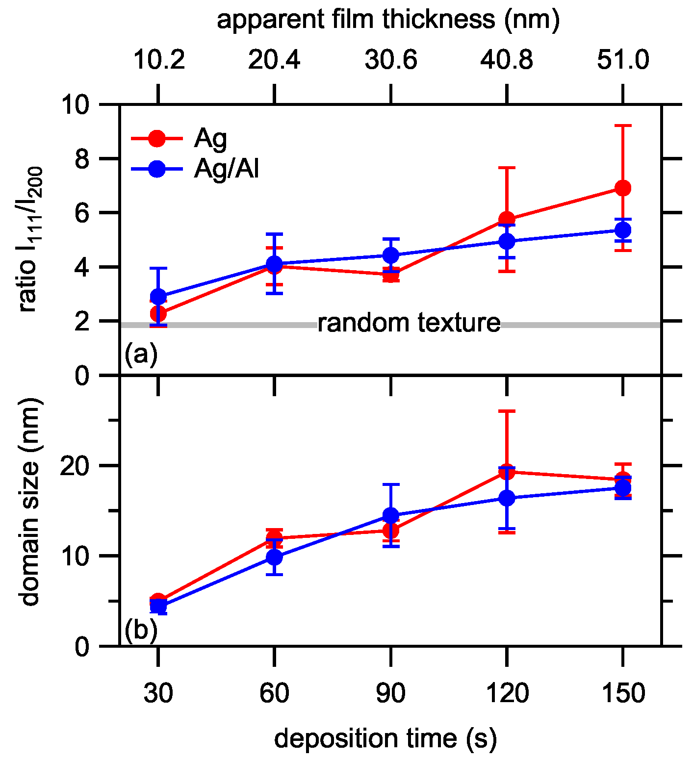
XRD patterns shows only (111) and (200) Bragg reflections (Figure 7). No other peaks are observed. The intensity ratio I 111 / I 200 is for all mean film thicknesses larger than for a random textured film which indicates that all films have a [111] out-of-plane fiber texture. The domain size increases with increasing film thickness. Similarly to the texture, no differences are observed between silver layers with and without Al seed layer.
Optical transmittance spectra (not shown) indicate slightly more transparent seeded silver layers, but above a mean thickness of approximately 20 nm (60 s of deposition) no differences between both films can be observed. The thinnest films show the typical plasmon appearance for discontinuous thin films [36].

3.5.2. Exposed Films

Figure 8 shows an overview of a SEM analysis of a corrosion spot for a non-seeded thin film with a nominal thickness of approx. 30 nm (90 s deposition) which was exposed to a 0.5 wt% HCl droplet. The analysis was performed in the aforementioned three rings (Figure 2). In the central region, the silver is agglomerated with the substrate exposed. The broader ring (position B) consists of agglomerated silver but the substrate is not yet visible. The smaller outer ring (position C) shows no silver agglomeration but small hillocks. Spots on seeded Ag layers showed the same features, and possible differences were difficult to quantify with SEM and/or AFM.

4. Discussion

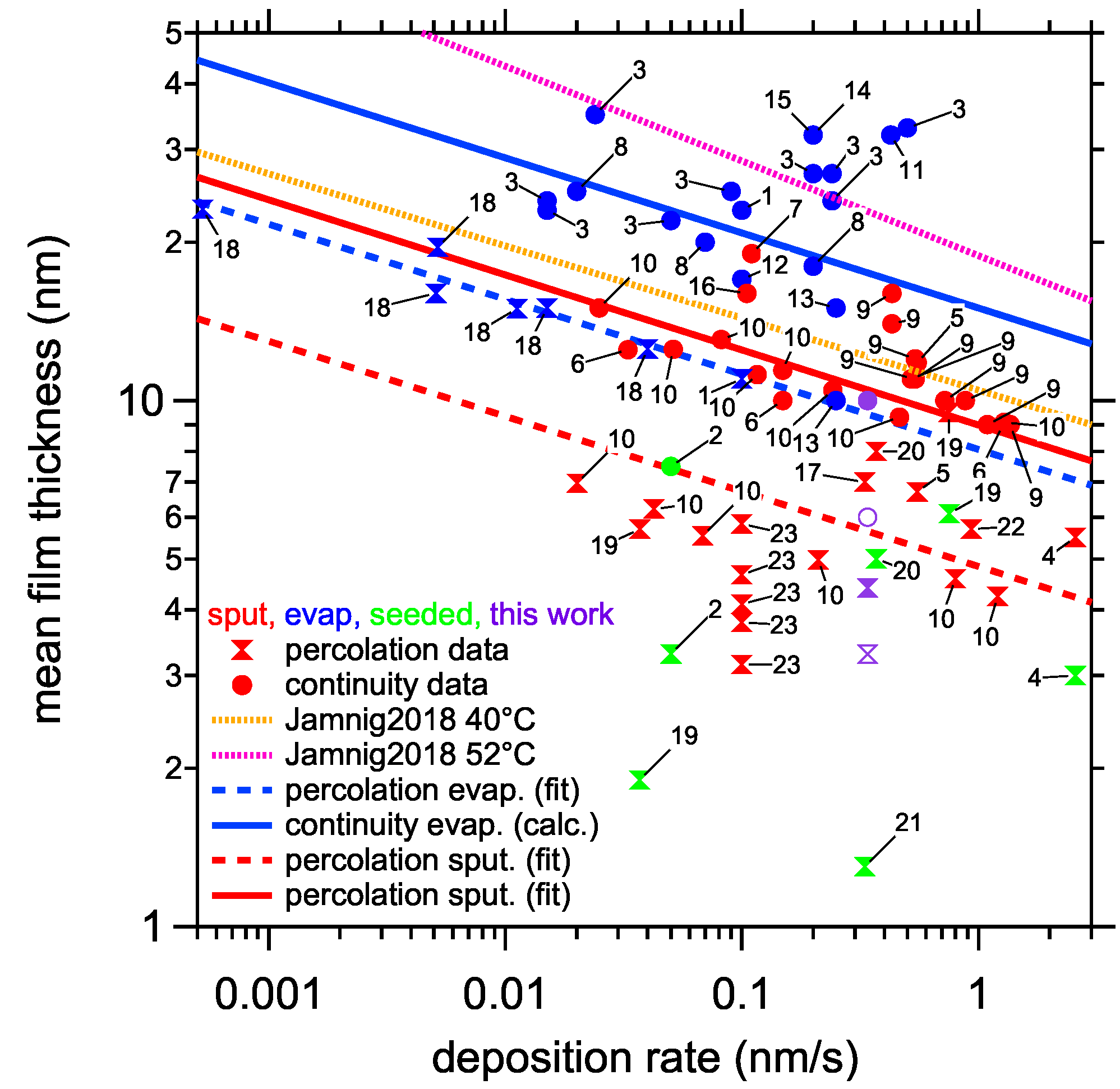
The growth of silver thin films on weakly-interacting substrates, such as glass or oxide covered silicon, has been reported in literature by many research teams. A good overview permits our results to be benchmarked against literature. The growth starts with the formation of nuclei or islands which grow until a connected network is formed. The formation of the connected network is characterized by a strong drop in the electrical resistivity, also known as the percolation threshold. An area filling factor of approximately 70% has been reported [37]. The holes in the network are further filled until a continuous thin film is formed. The continuity threshold can be determined from the tensile to compressive change of the incremental stress measured in situ during film growth [38]. Alternatively, as mentioned before, the continuity threshold can also be determined from the resistance(R)/film thickness ( t film ) measurement as the on-set for film continuity is connected with the minimum in the R t film 2 data versus the film thickness. The mean film thickness at the percolation and continuity threshold is mainly function of the substrate, deposition technique, substrate temperature, and deposition rate. An overview is shown in Figure 9. The percolation and continuity threshold for the films reported here are in agreement with the reported literature trends (see violet closed and open markers for non-seeded and seeded film, respectively).
From the compilation of these data, some interesting trends can be observed. According to Jamnig et al. [48] the influence of the deposition rate on the percolation and continuity threshold for sputter deposited thin films at room temperature follows a power law with an exponent of −1/7. The compilation for energetic deposition (red makers) confirms this trend. The ratio between the percolation and continuity threshold is approximately 1.9 ± 0.2. The value agrees well with the expected value (1.75) based on 2D percolation and a hole-filling mechanism of the formed network [62]. A similar trend can be extracted for the percolation threshold for non-energetic (thermal and e-beam evaporation) deposition (blue markers). The trend for the continuity threshold for these deposition techniques is less clear.
Based on the fitted result for the energetic deposition, and the assumption that the ratio between both thresholds is identical for both deposition strategies, the trend for the continuity threshold can be calculated (see striped blue line, Figure 9). Most data agree quite well with this trend. Additionally, two of the studies for sputtered silver films can be connected to this trend (see data points (7) [45] and two data points of the (9) series [47]). These experiments were performed at high deposition pressure which results in a low energy for the deposited atoms, similarly as for evaporation. One study (data series (3) [41] on Figure 9) strongly deviates from the calculated trend. A possible explanation is that the temperature control during these experiments was not successful and the experiments were performed at an actually higher temperature than intended. Indeed, the data fit better with the measured trends of Jamnig et al. [48] at higher deposition temperature (see purple line). Another trend which can be observed from the complied data is the lower threshold values for energetic deposition. This can be understood from ballistic effects, such as the break-up of smaller islands or the formation of surface defects, which increase the nucleation density. The study labeled as (23) [61] in Figure 9 is also interesting to mention as it compares the growth of silver layers on borosilicate glass covered with different types of oxides. It demonstrates that the percolation threshold depends on the substrate conditions as also demonstrated by others [63]. From the compilation it is clear that seeded layers results in a strong reduction in both thresholds. The presence of a seed layer results in a higher nucleation density, and, hence, the silver layer becomes continuous at smaller mean film thicknesses. Although this is the general trend, exceptions seem to exist. An evaluation of several seed layers showed that Ta and Cr seed layers had the reverse effect, i.e., a higher percolation threshold [64]. The same study showed that a thick seed layer (>0.1 nm) of Ni, Mo, and Zr resulted also resulted in a higher percolation threshold. The usage of a seed layer results according to most studies [65,66,67,68,69] in a smoother thin film.
The area of the corrosion spot linearly increases with time, which is characteristic for a diffusive behavior. This is in agreement with studies of the wetting behavior of droplets [70]. A very thin film of the order of 1 µm to 1 nm in thickness, known as the precursor film, spreads ahead of the central cap droplet. The length of the precursor increases as D f t , with D f a diffusion coefficient for the precursor, which agrees with the observations made in this study. To avoid a macroscopic change of the drop shape, and hence the results of the developed stability test, an alumina ring, which served as a “cup” for the droplet, was used in this study. In this way, the liquid spreading is limited to the precursor layer. According to hydrodynamic theory, the diffusion coefficient D f equals H / 3 π η h l i q with H the Hamaker constant, η the viscosity of the liquid, and h l i q the thickness of the precursor layer [71,72]. The Hamaker constant for Ag/H2O has been reported in a range between 30 and 400 × 10−21 J [73]. The viscosity of water at room temperature equals 1 mPa.s. Literature on the precursor layer thickness for water is hard to find. Studies on the adsorption of noble metals show that at high humidity the adsorption layer is a few monolayers thick, or in the order of a few nanometer [74,75]. Using the aforementioned values, diffusion coefficient equals to 0.01 to 0.13 mm2·s−1. The diffusion coefficients reported in this paper fit in this wide range. However, most of the studies have been performed for the spreading of Van der Waals liquid droplets under “dry” conditions, while, in this study, the spreading is performed under humid conditions. Moreover, as the silver thin film interacts with the acidic liquid, the behavior is probably more complicated. Indeed, the HCl concentrations are too low to strongly affect the water properties which define the liquid spreading. The diffusion coefficient depends however strongly on the HCl concentration. Hence, one can expect an interaction between the formation of the discontinuous layer and the liquid spreading. Nevertheless, studies on reactive wetting show similar behavior as reported here [76]. Additionally, the wetting behavior of the precursor layer can be influenced by the surface roughness. The behavior has only been described in the micron range [70]. According to the same study, the diffusion coefficient for the precursor layer scales with the roughness amplitude, and, hence, it can be expected that the foot spreads faster on a rough surface. This could explain the difference between the seeded and non-seeded films but the initial increasing growth rate of the affected area with increasing thickness for the non-seeded layers seems to conflict with this reasoning as the roughness initially decreases with film thickness. Further, the difference in RMS roughness between the two series is relatively small while the value for the diffusivity for the non-seeded layers is on average 3 times larger as compared to the seeded layers.
As mentioned in the Introduction, the dewetting of the silver layer or its conversion from a continuous layer to an agglomerated microstructure can be understood from the chemical attack of the grain boundaries which leads to the formation of hole which are unstable. Both seeded and non-seeded films have a similar crystallite size (see XRD results) which excludes a difference in grain boundary density as a possible explanation for the observed difference in stability. When the hole growth is controlled by surface diffusion, the growth rate is proportional with 1 / h 3 with h the film thickness [27,29]. Hence, thicker films are more stable. For the thinnest films, the seeded films contain fewer regions with lower thickness which enhances their stability (see AFM results). Nevertheless, the increasing diffusivity as function of the mean film thickness for non-seeded layers seems to oppose the above reasoning. Moreover, the non-seeded films with a thickness in the range of the maximum observed diffusivity have a similar roughness, height density distribution as the seeded layers. Further also the other studied properties, such as film resistivity, texture, and domain size, do not significantly differ between both series for these film thicknesses.
One possible reason for the influence of the seed layer can be a difference in the surface diffusivity of silver as the latter property affects the hole growth. It is fair to compare the surface diffusion rate under the given conditions with surface diffusion rates reported for silver in vacuo as the diffusion rate for Ag is hardly affected by the presence of water [77]. It has been reported that the activation energy for surface diffusion is much higher for Ag on other metal surfaces [78]. The latter study provides no information of the Al/Ag combination but a higher activation barrier for Ag on Cu is reported. Additionally, for layers seeded with Cu, an improved chemical stability has been reported [42]. As discussed in the introduction, another strategy to improve the stability of the silver layer is alloying. It is interesting to remark that also a lower surface diffusivity was used to explain the lower roughness of Al-doped Ag thin films [11], and that the addition of Cu to Ag reduces the surface diffusivity [79].
Another possible reason which can explain this difference in diffusivity is the intrinsic film stress. Using the same mechanism for agglomeration, Srolovitz and Goldinder [27] reason that presence of a stress of either sign within the film decreases the film stability. As the stored elastic energy density increases with increasing film thickness, the dewetting mechanism will be enhanced as the energy release will be an additional driving force. A similar reasoning was presented for epitaxial silver films deposited on silicon [80]. The increased film thickness, however, will also stabilize the film as discussed before. This could explain the observed maximum in the diffusivity for the non-seeded layers. A difference between germanium seeded and non-seeded silver layers regarding the stress evolution has been reported [81]. The final stress state, i.e., after relaxation of the incremental stress, was function of the lateral size of the surface features as measured with AFM (defined as the grain size in that study [81]) and the deposition rate. Increasing the deposition rate results in more compressive films, while larger surface features results in a more tensile films. Therefore, the difference in AFM surface features observed between non-seeded and seeded thin films (Figure 5) could result in a difference in the stress state which can influence the chemical dewetting behavior.

5. Conclusions

This study focuses on the chemical stability of seeded and non-seeded thin silver films. Silver films agglomerate under the influence of the chemical attack. Therefore, the stability was studied by measuring the growth rate of the agglomeration region. The area of the agglomerated region increases linearly with time. The difference in stability between non-seeded and seeded layers is not yet fully elucidated. Possible mechanisms are based on a difference in the surface diffusivity of silver and/or the stress state. Further research on the role of the material dependency of the seed layer and stress are, therefore, required to further unravel the details of the proposed mechanism.

Funding

This research received no external funding.

Data Availability Statement

All data can be obtained by a simple request to the author.

Conflicts of Interest

The author declares no conflict of interest.

References

  1. Vitelaru, C.; Parau, A.C.; Kiss, A.E.; Pana, I.; Dinu, M.; Constantin, L.R.; Vladescu, A.; Tonofrei, L.E.; Adochite, C.S.; Costinas, S.; et al. Silver-containing thin films on transparent polymer foils for antimicrobial applications. Coatings 2022, 12, 170. [Google Scholar] [CrossRef]
  2. Abbas, N.; Shad, M.R.; Hussain, M.; Mehdi, S.M.Z.; Sajjad, U. Fabrication and characterization of silver thin films using physical vapor deposition, and the investigation of annealing effects on their structures. Mater. Res. Express 2019, 6, 116437. [Google Scholar] [CrossRef]
  3. Martín-Palma, R.J.; Vázquez, L.; Martínez-Duart, J.M.; Malats-Riera, A. Silver-based low-emissivity coatings for architectural windows: Optical and structural properties. Sol. Energy Mater. Sol. Cells 1998, 53, 55–66. [Google Scholar] [CrossRef]
  4. Aguilar-Santana, J.L.; Jarimi, H.; Velasco-Carrasco, M.; Riffat, S. Review on window-glazing technologies and future prospects. Int. J. Low-Carbon Technol. 2019, 15, 112–120. [Google Scholar] [CrossRef]
  5. Park, H.K.; Kang, J.W.; Na, S.I.; Kim, D.Y.; Kim, H.K. Characteristics of indium-free GZO/Ag/GZO and AZO/Ag/AZO multilayer electrode grown by dual target DC sputtering at room temperature for low-cost organic photovoltaics. Sol. Energy Mater. Sol. Cells 2009, 93, 1994–2002. [Google Scholar] [CrossRef]
  6. Zhang, C.; Ji, C.; Park, Y.B.; Guo, L.J. Thin-metal-film-based transparent conductors: Material preparation, optical design, and device applications. Adv. Opt. Mater. 2020, 9, 2001298. [Google Scholar] [CrossRef]
  7. Lee, E.S. Spectrally Selective Glazings; Technical Report; New Technology Energy Management Program, Federal Energy Management Program: Washington, DC, USA, 1998. [Google Scholar]
  8. Ding, G.; Clavero, C. Silver based low emissivity coating technology for energy saving window applications. In Modern Technologies for Creating the Thin-Film Systems and Coatings; InTech: Vienna, Austria, 2017. [Google Scholar] [CrossRef] [Green Version]
  9. American Institute of Architects Continuing Education Systems. In The Value-Added Performance of Coated Glass; Technical Report; AIACES: New York, NY, USA, 2020.
  10. Bender, M.; Seelig, W.; Daube, C.; Frankenberger, H.; Ocker, B.; Stollenwerk, J. Dependence of film composition and thicknesses on optical and electrical properties of ITO–metal–ITO multilayers. Thin Solid Film. 1998, 326, 67–71. [Google Scholar] [CrossRef]
  11. Gu, D.; Zhang, C.; Wu, Y.K.; Guo, L.J. Ultrasmooth and thermally stable silver-based thin films with subnanometer roughness by aluminum doping. ACS Nano 2014, 8, 10343–10351. [Google Scholar] [CrossRef]
  12. Zhao, G.; Jeong, E.; Choi, E.A.; Yu, S.M.; Bae, J.S.; Lee, S.G.; Han, S.Z.; Lee, G.H.; Yun, J. Strategy for improving Ag wetting on oxides: Coalescence dynamics versus nucleation density. Appl. Surf. Sci. 2020, 510, 145515. [Google Scholar] [CrossRef]
  13. Jamnig, A.; Pliatsikas, N.; Abadias, G.; Sarakinos, K. Manipulation of thin metal film morphology on weakly interacting substrates via selective deployment of alloying species. J. Vac. Sci. Technol. A 2022, 40, 033407. [Google Scholar] [CrossRef]
  14. Shamsuddin, W.N.S.W.; Roccisano, A.; Zuber, K.; Murphy, P.J.; Jane, M.L. Environmentally robust Ag–Cu based low-E coatings. Sol. Energy Mater. Sol. Cells 2022, 248, 112033. [Google Scholar] [CrossRef]
  15. Nakanishi, Y.; Kato, K.; Omoto, H.; Yonekura, M. Correlation between microstructure and salt-water durability of Ag thin films deposited by magnetron sputtering. Thin Solid Film. 2013, 532, 141–146. [Google Scholar] [CrossRef]
  16. Jamnig, A.; Pliatsikas, N.; Konpan, M.; Lu, J.; Kehagias, T.; Kotanidis, A.N.; Kalfagiannis, N.; Bellas, D.V.; Lidorikis, E.; Kovac, J.; et al. 3D-to-2D morphology manipulation of sputter-deposited nanoscale silver films on weakly interacting substrates via selective nitrogen deployment for multifunctional metal contacts. ACS Appl. Nano Mater. 2020, 3, 4728–4738. [Google Scholar] [CrossRef]
  17. Hill, R.J.; Nadel, S.N. Coated Glass: Applications and Markets; BOC Coating Technology: Fairfield, CA, USA, 1999. [Google Scholar]
  18. Park, H.S.; Day, D.E. Corrosion of evaporated Ag films on glass by saturated water vapor. Sol. Energy Mater. 1986, 13, 351–365. [Google Scholar] [CrossRef]
  19. Ross, R.C. Observations on humidity-induced degradation of Ag-based low-emissivity films. Sol. Energy Mater. 1990, 21, 25–42. [Google Scholar] [CrossRef]
  20. Ando, E.; Miyazaki, M. Moisture degradation mechanism of silver-based low-emissivity coatings. Thin Solid Film. 1999, 351, 308–312. [Google Scholar] [CrossRef]
  21. Ando, E.; Miyazaki, M. Moisture resistance of the low-emissivity coatings with a layer structure of Al-doped ZnO/Ag/Al-doped ZnO. Thin Solid Film. 2001, 392, 289–293. [Google Scholar] [CrossRef]
  22. Wang, X.; Santschi, C.; Martin, O.J.F. Strong improvement of long-term chemical and thermal stability of plasmonic silver nanoantennas and films. Small 2017, 13, 1700044. [Google Scholar] [CrossRef] [Green Version]
  23. Yang, Z.; Wang, J.; Shao, Y.; Jin, Y.; Yi, M. Studying corrosion of silver thin film by surface plasmon resonance technique. Opt. Quantum Electron. 2019, 52, 31. [Google Scholar] [CrossRef]
  24. Sasaki, Y.; Kawamura, M.; Kiba, T.; Abe, Y.; Kim, K.H.; Murotani, H. Improved durability of Ag thin films under high humidity environment by deposition of surface Al nanolayer. Appl. Surf. Sci. 2020, 506, 144929. [Google Scholar] [CrossRef]
  25. Chen, S.W.; Bai, C.Y.; Jain, C.C.; Zhan, C.J.; Koo, C.H. Durability of indium tin oxide-silver-indium tin oxide films against moisture investigated through the wettability of the top oxide layer. Mater. Trans. 2007, 48, 2230–2234. [Google Scholar] [CrossRef] [Green Version]
  26. Han, G.C.; Wu, Y.H.; Luo, P.; Qiu, J.J.; Chong, T.C. Dewetting observations of ultrathin metallic films. Solid State Commun. 2003, 126, 479–484. [Google Scholar] [CrossRef]
  27. Srolovitz, D.J.; Goldiner, M.G. The thermodynamics and kinetics of film agglomeration. JOM 1995, 47, 31–36. [Google Scholar] [CrossRef]
  28. Agrawal, P.M.; Rice, B.M.; Thompson, D.L. Predicting trends in rate parameters for self-diffusion on FCC metal surfaces. Surf. Sci. 2002, 515, 21–35. [Google Scholar] [CrossRef]
  29. Srolovitz, D.J.; Safran, S.A. Capillary instabilities in thin films. II. Kinetics. J. Appl. Phys. 1986, 60, 255–260. [Google Scholar] [CrossRef]
  30. Koike, K.; Yamazaki, F.; Okamura, T.; Fukuda, S. Improvement of corrosion resistance of transparent conductive multilayer coating consisting of silver layers and transparent metal oxide layers. J. Vac. Sci. Technol. A Vac. Surf. Film. 2007, 25, 527–531. [Google Scholar] [CrossRef] [Green Version]
  31. Koike, K.; Shimada, K.; Fukuda, S. Aggregation in thin-film silver: Induced by chlorine and inhibited by alloying with two dopants. Corros. Sci. 2009, 51, 2557–2564. [Google Scholar] [CrossRef]
  32. Schneider, C.A.; Rasband, W.S.; Eliceiri, K.W. NIH Image to ImageJ: 25 years of image analysis. Nat. Methods 2012, 9, 671–675. [Google Scholar] [CrossRef] [PubMed]
  33. Miccoli, I.; Edler, F.; Pfnür, H.; Tegenkamp, C. The 100th anniversary of the four-point probe technique: The role of probe geometries in isotropic and anisotropic systems. J. Phys. Condens. Matter 2015, 27, 223201. [Google Scholar] [CrossRef]
  34. Maaroof, A.I.; Evans, B.L. Onset of electrical conduction in Pt and Ni films. J. Appl. Phys. 1994, 76, 1047–1054. [Google Scholar] [CrossRef]
  35. Nelson, A. Co-refinement of multiple-contrast neutron/X-ray reflectivity data using MOTOFIT. J. Appl. Crystallogr. 2006, 39, 273–276. [Google Scholar] [CrossRef]
  36. Axelevitch, A.; Gorenstein, B.; Golan, G. Investigation of optical transmission in thin metal films. Phys. Procedia 2012, 32, 1–13. [Google Scholar] [CrossRef] [Green Version]
  37. Wei, H.; Eilers, H. From silver nanoparticles to thin films: Evolution of microstructure and electrical conduction on glass substrates. J. Phys. Chem. Solids 2009, 70, 459–465. [Google Scholar] [CrossRef] [Green Version]
  38. Hoffman, R.W. Stresses in thin films: The relevance of grain boundaries and impurities. Thin Solid Film. 1976, 34, 185–190. [Google Scholar] [CrossRef]
  39. Abermann, R.; Koch, R. The internal stress in thin silver, copper and gold films. Thin Solid Film. 1985, 129, 71–78. [Google Scholar] [CrossRef]
  40. Chen, W.; Thoreson, M.D.; Ishii, S.; Kildishev, A.V.; Shalaev, V.M. Ultra-thin ultra-smooth and low-loss silver films on a germanium wetting layer. Opt. Express 2010, 18, 5124. [Google Scholar] [CrossRef]
  41. Del Vecchio, A.L.; Spaepen, F. The effect of deposition rate on the intrinsic stress in copper and silver thin films. J. Appl. Phys. 2007, 101, 063518. [Google Scholar] [CrossRef]
  42. Formica, N.; Ghosh, D.S.; Carrilero, A.; Chen, T.L.; Simpson, R.E.; Pruneri, V. Ultrastable and atomically smooth ultrathin silver films grown on a copper seed layer. ACS Appl. Mater. Interfaces 2013, 5, 3048–3053. [Google Scholar] [CrossRef] [PubMed]
  43. Grachev, S.; Hérault, Q.; Wang, J.; Balestrieri, M.; Montigaud, H.; Lazzari, R.; Gozhyk, I. A new method for high resolution curvature measurement applied to stress monitoring in thin films. Nanotechnology 2022, 33, 185701. [Google Scholar] [CrossRef]
  44. Jamnig, A.; Pliatsikas, N.; Sarakinos, K.; Abadias, G. The effect of kinetics on intrinsic stress generation and evolution in sputter-deposited films at conditions of high atomic mobility. J. Appl. Phys. 2020, 127, 045302. [Google Scholar] [CrossRef] [Green Version]
  45. Pliatsikas, N.; Jamnig, A.; Konpan, M.; Delimitis, A.; Abadias, G.; Sarakinos, K. Manipulation of thin silver film growth on weakly interacting silicon dioxide substrates using oxygen as a surfactant. J. Vac. Sci. Technol. A 2020, 38, 043406. [Google Scholar] [CrossRef]
  46. Kinosita, K.; Maki, K.; Nakamizo, K.; Takeuchi, K. Stress in vacuum deposited films of silver. Jpn. J. Appl. Phys. 1967, 6, 42–53. [Google Scholar] [CrossRef]
  47. Hérault, Q.; Gozhyk, I.; Balestrieri, M.; Montigaud, H.; Grachev, G.; Lazzari, R. Kinetics and mechanisms of stress relaxation in sputtered silver thin films. Acta Mater. 2021, 221, 117385. [Google Scholar] [CrossRef]
  48. Jamnig, A.; Sangiovanni, D.G.; Abadias, G.; Sarakinos, K. Atomic-scale diffusion rates during growth of thin metal films on weakly-interacting substrates. Sci. Rep. 2019, 9, 6640. [Google Scholar] [CrossRef] [Green Version]
  49. Wilcock, J.D.; Campbell, D.S.; Anderson, J.C. The internal stress in evaporated silver and gold films. Thin Solid Film. 1969, 3, 13–34. [Google Scholar] [CrossRef]
  50. Koch, R.; Winau, D.; Führmann, A.; Rieder, K.H. Growth-mode-specific intrinsic stress of thin silver films. Phys. Rev. B 1991, 44, 3369–3372. [Google Scholar] [CrossRef]
  51. Abermann, R.; Koch, R.; Kramer, R. Electron microscope structure and internal stress in thin silver and gold films deposited onto MgF2 and SiO substrates. Thin Solid Film. 1979, 58, 365–370. [Google Scholar] [CrossRef]
  52. Floro, J.A.; Hearne, S.J.; Hunter, J.A.; Kotula, P.; Chason, E.; Seel, S.C.; Thompson, C.V. The dynamic competition between stress generation and relaxation mechanisms during coalescence of Volmer-Weber thin films. J. Appl. Phys. 2001, 89, 4886–4897. [Google Scholar] [CrossRef] [Green Version]
  53. Seel, S.C. Stress and Structure Evolution during Volmer-Weber Growth of Thin Films. Ph.D. Thesis, Massachusetts Institute of Technology, Cambridge, MA, USA, 2002. [Google Scholar]
  54. Abadias, G.; Fillon, A.; Colin, J.J.; Michel, A.; Jaouen, C. Real-time stress evolution during early growth stages of sputter-deposited metal films: Influence of adatom mobility. Vacuum 2014, 100, 36–40. [Google Scholar] [CrossRef]
  55. Castillo, R.H.; Peñuñuri, F.; Canto-Reyes, D.; Borges Pool, A.; Mendez-Gamboa, J.A.; Acosta, M. Electrical percolation threshold evaluation of silver thin films for multilayer WO3/Ag/WO3 transparent conductive oxide. Mater. Lett. 2020, 260, 126913. [Google Scholar] [CrossRef]
  56. Lewowski, T. Photoelectron spectroscopy of thin discontinuous silver films deposited onto a sapphire substrate, near the percolation threshold. Thin Solid Film. 1995, 259, 53–58. [Google Scholar] [CrossRef]
  57. Byon, E.; Oates, T.W.H.; Anders, A. Coalescence of nanometer silver islands on oxides grown by filtered cathodic arc deposition. Appl. Phys. Lett. 2003, 82, 1634–1636. [Google Scholar] [CrossRef] [Green Version]
  58. Ko, R.H.H.; Khalatpour, A.; Clark, J.K.D.; Kherani, N.P. Ultrasmooth ultrathin Ag films by AlN seeding and Ar/N2 sputtering for transparent conductive and heating applications. APL Mater. 2018, 6, 121112. [Google Scholar] [CrossRef] [Green Version]
  59. Martínez-Cercós, D.; Paulillo, B.; Maniyara, R.A.; Rezikyan, A.; Bhattacharyya, I.; Mazumder, P.; Pruneri, V. Ultrathin metals on a transparent seed and application to infrared reflectors. ACS Appl. Mater. Interfaces 2021, 13, 46990–46997. [Google Scholar] [CrossRef]
  60. Santoro, G.; Yu, S.; Schwartzkopf, M.; Zhang, P.; Vayalil, S.K.; Risch, J.F.H.; Rübhausen, M.A.; Hernández, M.; Domingo, C.; Roth, S.V. Silver substrates for surface enhanced Raman scattering: Correlation between nanostructure and Raman scattering enhancement. Appl. Phys. Lett. 2014, 104, 243107. [Google Scholar] [CrossRef] [Green Version]
  61. Hafezian, S. Growth Control and Study of Ultrathin Silver Films for Energy-Saving Coatings. Ph.D. Thesis, Polytechnique Montréal, Montreal, QC, Canada, 2019. [Google Scholar]
  62. Šmilauer, P. Thin metal films and percolation theory. Contemp. Phys. 1991, 32, 89–102. [Google Scholar] [CrossRef]
  63. Goetz, S.; Bauch, M.; Dimopoulos, T.; Trassl, S. Ultrathin sputter-deposited plasmonic silver nanostructures. Nanoscale Adv. 2020, 2, 869–877. [Google Scholar] [CrossRef]
  64. Fukuda, K.; Lim, S.H.N.; Anders, A. Coalescence of magnetron-sputtered silver islands affected by transition metal seeding (Ni, Cr, Nb, Zr, Mo, W, Ta) and other parameters. Thin Solid Film. 2008, 516, 4546–4552. [Google Scholar] [CrossRef]
  65. Logeeswaran, V.J.; Kobayashi, N.P.; Islam, M.S.; Wu, W.; Chaturvedi, P.; Fang, N.X.; Wang, S.Y.; Williams, R.S. Ultrasmooth silver thin films deposited with a germanium nucleation layer. Nano Lett. 2009, 9, 178–182. [Google Scholar] [CrossRef] [PubMed]
  66. Liu, H.; Wang, B.; Leong, E.S.P.; Yang, P.; Zong, Y.; Si, G.; Teng, J.; Maier, S.A. Enhanced surface plasmon resonance on a smooth silver film with a seed growth layer. ACS Nano 2010, 4, 3139–3146. [Google Scholar] [CrossRef] [PubMed]
  67. Colenso, H.R.; Rafealov, E.Z.; Maddah, M.; Plank, N.O.V.; Chen, W.T.; Waterhouse, G.I.N.; Hao, J.; Gouws, G.J.; Moore, C.P. Comparison of seed layers for smooth, low loss silver films used in ultraviolet-visible plasmonic imaging devices. Thin Solid Film. 2018, 656, 68–74. [Google Scholar] [CrossRef]
  68. Sonmez, N.A.; Donmez, M.; Comert, B.; Ozcelik, S. Ag/M-seed/AZO/glass structures for low-E glass: Effects of metal seeds. Int. J. Appl. Glass Sci. 2017, 9, 383–391. [Google Scholar] [CrossRef]
  69. Ciesielski, A.; Skowronski, L.; Trzcinski, M.; Szoplik, T. Controlling the optical parameters of self-assembled silver films with wetting layers and annealing. Appl. Surf. Sci. 2017, 421, 349–356. [Google Scholar] [CrossRef]
  70. Cazabat, A.M. How does a droplet spread? Contemp. Phys. 1987, 28, 347–364. [Google Scholar] [CrossRef]
  71. Joanny, J.F.; de Gennes, P.G. Upward creep of a wetting fluid: A scaling analysis. J. Phys. 1986, 47, 121–127. [Google Scholar] [CrossRef]
  72. Shiomoto, S.; Higuchi, H.; Yamaguchi, K.; Takaba, H.; Kobayashi, M. Spreading dynamics of a precursor film of ionic liquid or water on a micropatterned polyelectrolyte brush surface. Langmuir 2021, 37, 3049–3056. [Google Scholar] [CrossRef]
  73. Pinchuk, A.O. Size-dependent Hamaker constant for silver nanoparticles. J. Phys. Chem. C 2012, 116, 20099–20102. [Google Scholar] [CrossRef]
  74. Demirdjian, B.; Bedu, F.; Ranguis, A.; Ozerov, I.; Henry, C.R. Water adsorption by a sensitive calibrated gold plasmonic nanosensor. Langmuir 2018, 34, 5381–5385. [Google Scholar] [CrossRef] [PubMed] [Green Version]
  75. Guo, L.Q.; Zhao, X.M.; Bai, Y.; Qiao, L.J. Water adsorption behavior on metal surfaces and its influence on surface potential studied by in situ SPM. Appl. Surf. Sci. 2012, 258, 9087–9091. [Google Scholar] [CrossRef]
  76. Kawaguchi, M.; Hamada, H. Reactive wetting by liquid sodium on thin Au plating. J. Nucl. Sci. Technol. 2013, 51, 201–207. [Google Scholar] [CrossRef]
  77. Porter, J.D.; Robinson, T.O. Surface diffusion of silver at the silver (111)/liquid-water interface from electrocrystallization measurements. J. Phys. Chem. 1993, 97, 6696–6709. [Google Scholar] [CrossRef]
  78. Sanders, D.E.; DePristo, A.E. Predicted diffusion rates on fcc (001) metal surfaces for adsorbate/substrate combinations of Ni, Cu, Rh, Pd, Ag, Pt, Au. Surf. Sci. 1992, 260, 116–128. [Google Scholar] [CrossRef]
  79. Han, H.; Zoo, Y.; Mayer, J.W.; Alford, T.L. Improved surface morphology and texture of Ag films on indium tin oxide via Cu additions. J. Appl. Phys. 2007, 102, 036101. [Google Scholar] [CrossRef]
  80. Baburin, A.S.; Ivanov, A.I.; Lotkov, E.S.; Sorokina, O.S.; Boginskaya, I.A.; Sergeev, E.V.; Buzaverov, K.A.; Konstantinova, T.G.; Moskalev, D.O.; Issabayeva, Z.; et al. Epitaxial silver films morphology and optical properties evolution over two years. Coatings 2020, 10, 911. [Google Scholar] [CrossRef]
  81. Flötotto, D.; Wang, Z.M.; Jeurgens, L.P.H.; Mittemeijer, E.J. Kinetics and magnitude of the reversible stress evolution during polycrystalline film growth interruptions. J. Appl. Phys. 2015, 118, 055305. [Google Scholar] [CrossRef]
Figure 1. Set-up to measure the degradation spot formation. The tube is cut open to show the set-up interior and the sample holder. The light source (not shown) is cooled with a ventilator (not shown) to avoid heating and water condensation.
Coatings 12 01915 g001
Figure 2. The growth of the degradation spot. Experimental conditions: silver thickness is approximately 17 nm (50 s deposition). HCl concentration equals 0.5 wt%. (a) Images taken at an interval of 45 s. (b) Difference between the last image and first image. The spot consists of three different concentric rings: a large central ring (1), followed by a less broad ring (2), and a final ring which is at the rim of the degradation spot (3). (c) The area of the degradation spot as function of time. The blue line is a linear fit to the data. The slope of the line is D which equals in this case 0.183 mm2/s.
Coatings 12 01915 g002
Figure 3. Influence of the film thickness/deposition time on the diffusivity for silver thin films deposited on glass without seed layer (red) and with an Al seed layer (blue). The green line is a smoothed spline through the data points related to the growth rate of the corrosion spot. The ratio of the resistivity, as measured ex situ using a Van der Pauw set-up, between film deposited with and without seed layer is shown on the right hand axis (purple points and line (only to guide the eyes)).
Coatings 12 01915 g003
Figure 4. SEM top view of thin films deposited on silicon. Top images (a,b) show SEM top view images of non-seeded Ag layers with a nominal thickness of 3 nm and 6 nm, respectively. Bottom images (c,d) show SEM top view images of seeded Ag layers with the same nominal thickness as (a,b). The Al seed layer has a nominal thickness of 0.5 nm.
Coatings 12 01915 g004
Figure 5. The height distribution for non-seeded Ag (red) and seeded Ag (blue) films as measured by AFM within a region of 5 μ m × 5 μ m. The top right figure displays the RMS average roughness as function of the mean film thickness. The images (top) are AFM height profiles within a 1 μ m × 1 μ m region for non-seeded and seeded layers with a mean film thickness of 31 nm.
Coatings 12 01915 g005
Figure 6. XRR patterns for silver film deposited on Si without (left) and with (right) Al seed layer. The silver films were deposited for 30 s, 60 s, and 90 s, and the aluminum layer for 15 s. This results in Ag films of approximately 10, 20, and 30 nm and a Al film of 0.5 nm. The color traces show the experiments, while the black lines are simulated patterns using Motofit [35].
Coatings 12 01915 g006
Figure 7. (a). The ratio between the diffraction intensity of the (111) and (200) Bragg reflection as function of the deposition time (or apparent film thickness). The grey line indicates the same ratio for a random textured silver film. (b). The domain size as calculated from the integral breath of the (111) Bragg reflection. The Al seed layer has a nominal thickness of 0.5 nm. All films were deposited and analyzed three times.
Coatings 12 01915 g007
Figure 8. SEM analysis of the corrosion spot (deposition time 90 s without seed layer exposed to 0.5 wt% HCl). The sample was studied using SEM at the center of the colored circles, labeled A, B and C, indicated on the digital microscope image shown at the left.
Coatings 12 01915 g008
Figure 9. Reported percolation (hourglass symbols) and continuity (round) thresholds for silver thin films deposited at room temperature using different techniques. Red symbols are for energetic techniques (mainly sputtering), while blue symbols are for evaporation and e-beam experiments. Green markers are for seeded layers. The seed material is mentioned in the reference list. The full (striped) blue and red lines are fitted (calculated) power laws with an exponent −1/7 (see text). The orange and purple lines are reproduced from the work of Jamnig et al. for films deposited at 40 and 52 °C, respectively. The violet markers are used for this work (full and open marker for non-seeded and seeded layer, respectively). Data taken from: (1) [39], (2(Ge)) [40], (3) [41], (4(Cu)) [42], (5) [43], (6) [44], (7) [45], (8) [46], (9) [47], (10) [48], (11) [49], (12) [50], (13) [51], (14) [52], (15) [53], (16) [54], (17) [55], (18) [56], [19(ZnO)] [57], (20) [58], (21(CuO)) [59], (22) [60], and (23) [61].
Coatings 12 01915 g009
Publisher’s Note: MDPI stays neutral with regard to jurisdictional claims in published maps and institutional affiliations.