1. Introduction
The most effective way of modifying the surface of materials is through the deposition of thin-film, 0.01–50 µm, coatings of various materials with a given structure and property [
1,
2]. Such coatings essentially change the mechanical, optical, electrical, magnetic, thermal, and chemical properties of the original material, producing in the end a product with the required properties [
3]. The advance in this research field that relies on using simple materials (conductive metal- and alloy-based coatings [
4], oxide, nitride and carbide [
5,
6] coatings) has almost reached its limitations. Further progress in this area is deemed possible by switching to the use of composite (hybrid) materials that combine the best properties of their components. The creation of hybrid materials involves a number of issues, such as matching the interface properties of different materials, deposition technique, among others.
The fabrication of quality ceramic-based dielectric coatings is a topical problem, since such coatings provide all above properties and are inexpensive to produce. Ceramic coatings are usually manufactured in the form of thin and fragile layers that are prone to cracking, and, under cyclic thermal load, to peeling [
7]. At the same time, these coatings exhibit high resistance to corrosion [
8] and oxidation [
9]. Ceramics is used in the parts subject to static loads, i.e., combustion chamber linings [
10], in medical equipment [
11] and aerospace industry [
12]. With regard to microelectronics, ceramic coatings can be used to provide the necessary heat conductivity of integrated circuits elements, while preserving their electrical insulation [
13,
14]. Ceramic coatings are often fabricated as complex silicates with additions of ZrО
2, ТiO
2, А1
2О
3, СеО
2, etc., capable of protecting the substrate material against temperatures as high as 1300 °С [
15].
Today, among the most popular methods for obtaining dielectric and, in particular ceramic coatings, are ion-plasma [
16] and beam [
17] technologies. The most widespread methods of ion-plasma technologies are magnetron sputtering [
18], systems based on a vacuum arc [
19], and plasma-chemical methods [
20]. All these methods have their pros and cons; they have been successfully used to obtain metal- and alloys-based coatings for a long time. However, to obtain ceramic coatings, one has to invent sophisticated solutions, which, as a consequence, lead either to a drastic decrease in the productivity of the deposition process, or to a significant deterioration in the quality of the coatings [
21]. Beam technologies (laser radiation or electron beam) are based on the evaporation of the target material by energy fluxes and condensation of the vapors on the substrate [
22,
23]. Laser technologies are used to obtain coatings in a wide range of gas pressures (up to atmospheric), and during the evaporation of various target materials, including dielectric materials [
24]. A feature of the laser is its high-power density in a focused spot of laser radiation, reaching hundreds of kilowatts per square centimeter.
When the target material is heated by a power density, exceeding the threshold value, an explosive boiling of the target material occurs, leading to the contamination of the flow of the evaporated material with a droplet fraction; in addition, there is a problem of dusting the optical radiation input window, as well as screening the target surface with vapors of the evaporated material. In addition, there is a relatively low efficiency of the laser systems themselves. The use of an electron beam to create dielectric coatings requires solving the problem of neutralizing the charging of the surface of a dielectric target by an electron beam [
25]. Therefore, despite the multitude of methods and techniques for the synthesis of dielectric coatings, none of them fully meets the requirements for efficient and quality deposition. The fore-vacuum plasma cathode electron sources developed in recent decades [
25] provide the generation of electron beams in the range of elevated pressure from units to a hundred of pascals. In the fore-vacuum range, the negative charge carried over by the electron beam onto the dielectric surface is neutralized by the flux of positive ions from the beam plasma, providing in this way an effective action of the electron beam on the dielectric surface almost indistinguishable from the action of accelerated electrons on an electrically conductive metal surface. The electron beam capability of heating temperature resistant dielectric targets (ceramics, boron, etc.) up to melting temperatures is a promising feature that can be employed for depositing multi-functional dielectric coatings. In our earlier works, we have already shown the effectiveness of this method for deposition of coatings based on ceramics of various compositions, and have shown that the coatings, obtained by this method, have all the necessary properties for their use in modern technologies [
26,
27]. In the present article, we present the results of investigations aimed at a more detailed study of the parameters and characteristics of this process and particular properties of deposited coatings as applied to microelectronics.
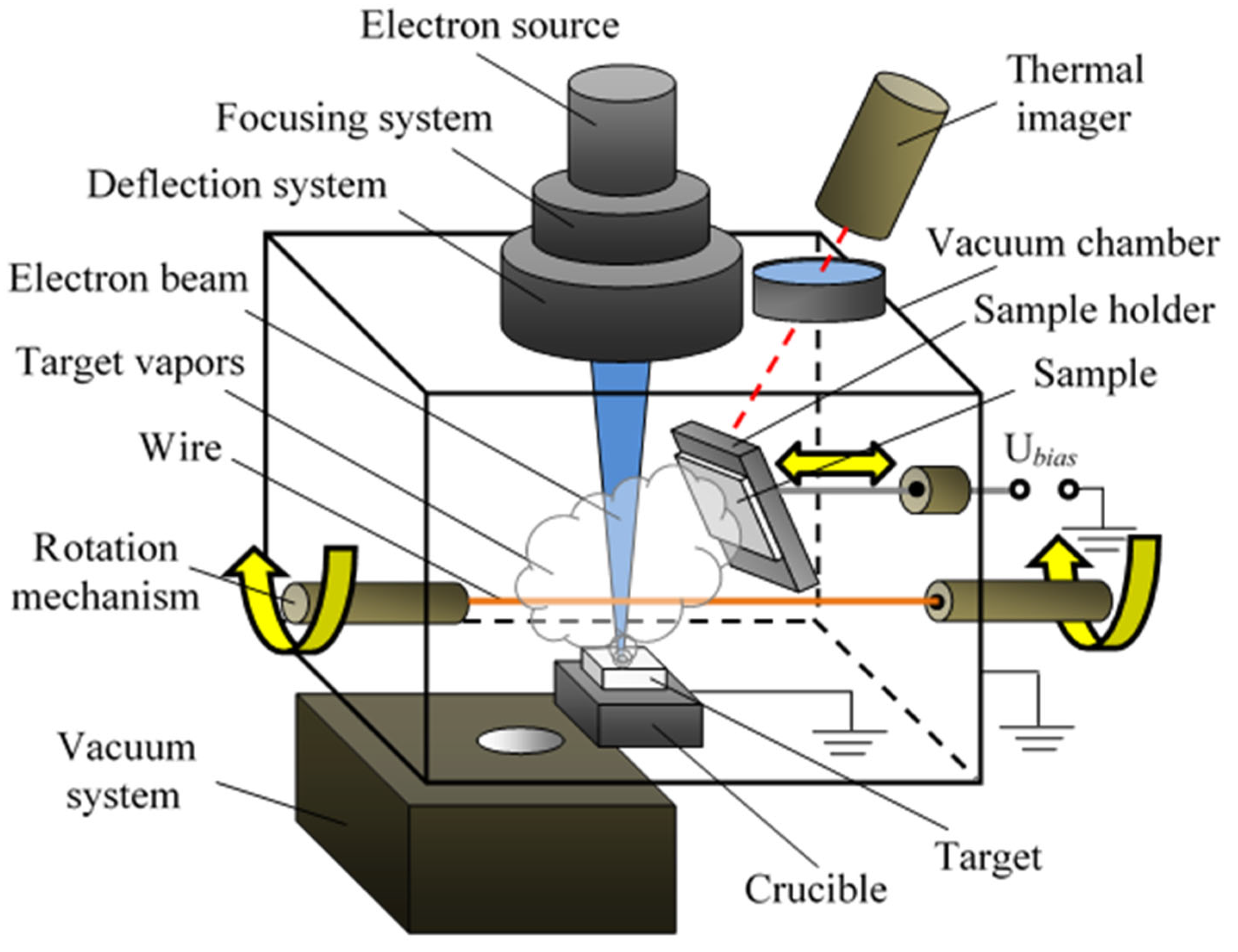
2. Experimental Setup
The experimental setup included a fore-vacuum plasma-cathode electron source, the working principle of which is based on the electron emission from a hollow-cathode discharge plasma (
Figure 1). The source provided the generation of a continuous electron beam in the pressure range of 1–100 Pa, at an accelerating voltage of 20 kV, the maximum discharge current of 1.5 A, and the beam current of 450 mA. With the beam focused to a 0.5 mm diameter, the maximum beam power reached 50 kW/cm
2. A more detailed description of the experimental setup and the electron source are given in [
28].
The vacuum chamber was evacuated to the base residual pressure of 1 Pa using a BОС Edwards E2M80 (Edwards Ltd., Burgess Hill, West Sussex, UK) two-stage rotary vane pump at 20 L/s. After reaching the base pressure, the vacuum system was flushed with a flow of pure helium injected into the chamber through an adjustable needle leak valve. Helium also served as a working gas for the electron source. Electron beams with different power densities transported through the vacuum chamber and focused on the target made of commercial alumina ceramics of different composition with dimensions 1 × 1 × 1 cm3. At a certain magnitude of the power density, the target material began to evaporate. Vapor of the target material deposited on a steel substrate, placed on a movable holder, as well as on a copper wire. The substrate temperature was monitored remotely using an optical pyrometer. To ensure a uniform coating deposition on the wire surface, the setup included a rotation mechanism. The rotation speed was chosen from the need to ensure the condition of multiple passage of the sample during the deposition of the coating on its surface and was set to be equal to 1 revolution per second. Before the deposition, the surface of the substrate was polished by an MP-1C grinding and polishing machine (Laizhou Lyric Testing Equipment Co., Ltd., Laizhou, Shandong, China) having a grinding disc with diameter of 230 mm, an adjustable grinding and polishing speed of 50–1000 rpm, equipped by a semi-automatic holder for 3 samples with a diameter of 30 mm.
A Hitachi S3400N scanning electron microscope (Hitachi-Science & Technology, Berkshire, UK) was used to obtain surface images of the coatings. The coating thickness was determined using a remote optical profilometer Profilm3D (Filmetrics, San Diego, CA, USA). A Pinon Disc and Oscillating TRIBO tester (IBOtechnic, Clichy, France) was used to measure the tribological properties of the coatings at room temperature (23 °C). This instrument employs the ‘ball on disk’ measuring technique. A tested sample is subject to a load of 2 N exerted by a ball tip made of aluminum oxide. The adhesive properties of coatings were determined by the scratch-off method [
29] based on an MST-S-AX-0000 micro-scratch tester (Centre Suisse d’Electronique et de Microtechnique, CSEM, Nevshatel, Switzerland).
The electrical insulating properties of the coating deposited on the copper wire were tested by a wire-pellet electrode system [
30]. The samples used in the wire-pellet test were strait wire sections with a length of at least 350 mm.
Figure 2 shows a bath with steel pellets used for testing.
In this test, we used a copper wire with a diameter of 0.8 mm insulated with a ceramic coating, and a wire of the same diameter with enamel insulation typically used for transformer windings. The test consisted of two stages. In the first stage, the test of breakdown voltage was carried out in the pellet bath. The testing technique was as follows. A prepared sample was placed in the pellet bath so that the thickness of the surrounding pellet layer was at least 5 mm. The length of the sample placed in the pellet was 125 mm. The pellet bath was installed in a high-voltage unit used for insulation breakdown. A high voltage was applied to the sample, as shown in
Figure 2, between the wire and the pellet. A high voltage of AC current of commercial frequency was applied to the sample. Upon the insulation breakdown, the overcurrent relay triggers, and the installation turns off, fixing the voltage value at which the breakdown occurs. The tests were carried out at room temperature.
In the second stage, we studied the effect of corona discharges on the average time to the breakdown under a prolonged application of the commercial frequency voltage. A part of the sample wire with a length of 125 mm was placed in the pellet and a voltage of 4–5 kV was applied. The lower limit of the voltage ensures the onset of ionization processes and the appearance of the surface discharges in the space between the wire and the pellet. The upper voltage limit is not large enough to break down an intact, defect-free insulation. The wire samples were exposed to the applied voltage until the breakdown occurred. The installation had a timer that set the time to the breakdown. For the final result, we took the insulation breakdown time averaged over five wire samples. The tests were carried out at room temperature.
3. Results and Discussion
The experimental dependences of the ceramic target mass removal rate on the beam power density are shown in
Figure 3. As seen from the presented dependences, the evaporation rate increases with the increase in beam power density, which can be related to both increasing temperature in the melting pool and expansion of the melting surface area.
The experiments show that, for the electron-beam evaporation of alumina-based ceramics, there exists a maximum beam power density that still ensures the formation of a uniform coating on the substrate surface (
Figure 4a).
When the beam power density exceeds a threshold value, an intensive boiling-up of the ceramics in the melting pool area occurs with the formation of splashes and droplets that deposit on the substrate (
Figure 4b). The explosive character of the ceramic target boiling-up under the electron-beam heating in fore-vacuum when the beam power exceeds the threshold level was observed for all alumina ceramics tested in the experiments. The magnitude of the threshold power density depends on the ceramic composition, the area of the melting pool, the beam current and energy. The threshold power density for different alumina-based ceramics varied in the range from 1 to 10 kW/cm
2, depending on the composition of a particular ceramics and its thermal properties, with the optimal maximum evaporation rate (without explosive boiling-up) being 5 g/h. The beam power densities were estimated experimentally taking into account the electron source emission current, accelerating voltage, and the visible beam diameter at the focal point. The lower limit for the beam power density typically corresponded to the regime with a uniform coating surface at a reasonable deposition rate, the upper limit characterized the over-intensive “boiling” of the target with large droplets and splashes on the deposited coating surface.
The existence of the threshold of the electron beam power density for a given ceramic material signifies the existence of the physical limit imposed on the conditions under which it is still possible to obtain a uniform ceramic coating by evaporating a ceramic target with an electron beam in fore-vacuum [
31].
Figure 5 shows the result of experiments on the deposition of coatings based on alumina ceramics on steel substrates with a diameter of 2 cm. The substrate size was chosen to fit the requirements of coating diagnostic devices. A potential from 0 to −100 V was applied to the substrate, and the deposition duration was one minute. Zero potential corresponded to the potential of the grounded vacuum chamber; at potentials lower than −100 V, we observed a gas discharge between the biased part and chamber walls. The experiments showed that the coating deposition rates depend on the potential applied to the sample. However, it should be noted that, for a potential lower than −25 V, its effect on the deposition rate is insignificant due to the formation of a thick layer on the entire surface of the sample and the vanishing potential in the vicinity of the sample. The coating deposition rates versus the substrate potential are shown in
Figure 5.
Figure 6, as an example, shows the measurements of the wear resistance of a steel sample (
Figure 6а) and the same sample with a deposited alumina-based coating (
Figure 6b).
The coating was deposited on the sample surface for one minute, the thickness was about 2 µm, and the substrate temperature did not exceed 500 °C. The wear rate of the original sample was 5 × 10
−4 mm
3/N·m at a friction coefficient of 0.789. The wear rate of the ceramic-coated sample was 0.79 × 10
−4 mm
3/N·m at a friction coefficient of 0.716. The significant increase in the wear resistance is associated with a decrease in the surface roughness after coating—a fact reported previously in our works [
17].
Figure 7 shows the measurements of the adhesion of a ceramic-coated sample of tool steel.
Figure 8 shows micrographs of the surface taken with an optical microscope at different loads
F exerted on a diamond indenter with a radius of 100 µm.
It can be seen from the results shown in
Figure 7 and
Figure 8 that, as the load on the indenter increases, it begins to smoothly deepen into the coating. As the indenter sinks into the material, the fiction coefficient increases, which speaks for the increase in the resistance to motion from the side of the sample. At a load F = 1.5 N, the first fluctuations of the friction coefficient become noticeable, which is a sign of irreversible changes in the surface structure. The indenter begins to sink deeper and the acoustic sensor registers the first vibrations. In the micrograph corresponding to a load of 3.5 N, one can observe the beginning of the film peeling process (
Figure 8c). As the load on the indenter increases, the fluctuations of the fiction coefficient increase and the indenter sinks deeper, which is a sign that the film starts to peel off the substrate and the indenter falls into the formed micro protrusions causing strong fluctuations of the fiction coefficient. In the micrograph (
Figure 8d) corresponding to a higher load (
F = 4.5 N), one can observe the appearance of a series of ring-shaped bulges under the exertion of lateral compressive stress from the penetrating conical indenter, which is indicative of the loss of stability and film peeling off the substrate.
Thus, for alumina-based coatings, destruction occurred under a load on the indenter from 4.5 to 8 N depending on the type of ceramics. The specific work of peeling ranged from 2.6 to 8.1 J/m2.
Table 1 shows the value of breakdown voltage for conventional enamel and ceramic insulation of copper wires, averaged over five wires.
As seen from
Table 1, the breakdown test results are close to both types of insulation coatings.
The dielectric strength tests can be carried out by placing a wire sample in an electrical discharge environment. When a high voltage is applied to the pellet, electrical discharges are formed over the entire surface of the insulated wire. The discharges gradually destroy the insulation and cause its breakdown. The average times to the breakdown of wire samples are given in
Table 2.
The obtained results clearly show a small difference in the resistance of a copper wire with ceramic coating insulation and a wire with enamel insulation to the breakdown voltage and the corona discharge ignited at the alternating voltage of industrial frequency. It demonstrates the good electrical insulation properties of the obtained coatings, making them suitable for insulation purposes in microelectronics.
As another example of the use of ceramic coatings in microelectronics, we deposited a ceramic-based coating on a monolithic integrated circuit (MIC) based on vertical Schottky diodes (
Figure 9). Note that the deposition of Al
2O
3-based coatings was carried out on the MIC whose active regions were passivated with a Si
3N
4 dielectric. This allows us to conclude that using Al
2O
3 coatings as a structural material for passivated microwave MICs is possible.
As seen from experimental data (
Figure 10), the ceramic-based coating does not increase mixer conversion losses in the high frequency range. Insignificant differences in the lower frequency range (4–16 GHz) may be attributed to instrumental measurement uncertainty.
No significant changes in LO/RF channel isolation are observed. The experiments carried out showed that the technique of ceramic-based deposition of coatings is compatible with the technology of manufacturing microwave MICs.
4. Conclusions
The presented method of electron-beam evaporation of ceramic targets with the subsequent deposition of their vapors on the substrate makes it possible to form dielectric coatings with a thickness of up to a few micrometers. The features of the process of deposition of dielectric coatings were revealed. It was found experimentally that, in the fore-vacuum pressure range, the optimal electron beam power density for electron beam evaporation of alumina is 1–30 kW/cm2, depending on the elemental composition of the particular material being evaporated.
It was established that, at the electron beam power density, optimal for electron beam evaporation of alumina-based ceramics (1–10 kW/cm2), the maximum evaporation rate is 5 g/h, and the coating deposition rate is about 0.5 µm/min, which is higher than the rates for other beam-plasma methods. Increasing the electron beam density power above optimum values brings about the explosive boiling-up of the target material and the contamination of the flux of the evaporated material with a droplet fraction, while a decrease in the power density decreases the evaporation rate. The elemental composition of the dielectric coatings matches that of the evaporated alumina sample, with the coating thickness reaching several microns. The deposition of coatings with good adhesion on a metal base by electron-beam evaporation of alumina ceramics decreases the surface roughness by 1.5–2.0 times and increases microhardness, and also significantly increases the wear resistance of the material. The obtained coatings can be used to insulate the surface of metal products, because the dielectric characteristics of the coatings are not inferior to standard modern insulation. Ceramic-based coatings deposited on microwave MICs can be used as protective and insulating, since they do not impair the chip operational characteristics.


