Article

Phase Control Growth of InAs Nanowires by Using Bi Surfactant

1
Institute of Physics, The Islamia University of Bahawalpur, Bahawalpur 63100, Pakistan
2
Centre of Excellence for Solid State Physics, University of Punjab, Lahore 54590, Pakistan
3
Office of the Controller of Examination, National Skills University Islamabad, Islamabad 44000, Pakistan
*
Author to whom correspondence should be addressed.
Coatings 2022, 12(2), 250; https://doi.org/10.3390/coatings12020250
Submission received: 20 January 2022 / Revised: 6 February 2022 / Accepted: 11 February 2022 / Published: 15 February 2022
(This article belongs to the Special Issue Coatings for Energy Efficient Buildings)

Abstract

:
To realize practical applications of nanowire-based devices, it is critical, yet challenging, to control crystal structure growth of III-V semiconductor nanowires. Here, we demonstrate that controlled wurtzite and zincblende phases of InAs nanowires can be fabricated using bismuth (Bi) as a surfactant. For this purpose, catalyst free selective area epitaxial growth of InAs nanowires was performed using molecular beam epitaxy (MBE). During the growth, Bi was used which may act as a wetting agent influencing the surface energy at growth plane ends, promoting wurtzite crystal phase growth. For a demonstration, wurtzite and zincblende InAs nanowires were obtained with and without using Bi-flux. Photoluminescence spectroscopy (PL) analysis of the nanowires indicates a strong correlation between wurtzite phase and the Bi-flux. It is observed that the bandgap energy of wurtzite and zincblende nanowires are ∼0.50 eV and ∼0.42 eV, respectively, and agree well with theoretical estimated bandgap of corresponding InAs crystal phases. A blue shift in PL emission peak energy was found with decreasing nanowire diameter. The controlled wurtzite and zincblende crystal phase and its associated heterostructure growth of InAs nanowires on Si may open up new opportunities in bandgap engineering and related device applications integrated on Si. Furthermore, this work also illustrates that Bi as a surfactant could play a dynamic role in the growth mechanism of III-V compound semiconductors.

1. Introduction

Semiconductor nanowires (NWs) have been a prevailing subject matter in the nanoscience community over recent decades due to their potential in building next generation electronics, optoelectronics and sensing devices [1,2,3]. More specifically, due to their distinct 1D nanoscale nature with diameter below 100 nm and large surface to volume ratio, they offer unique optical and electronic transport properties. Among III-V compound semiconductors, InAs has drawn special attention due to its small effective mass, high electron mobility and particularly its narrow direct bandgap. Furthermore, InAs NWs have enhanced thermoelectric performance, high Seebeck coefficient at room temperature, over that of bulk InAs, and can be further enhanced using diluted bismide [4,5,6]. Exploiting the use of InAs NWs for thermoelectric generators can efficiently convert heat energy into electrical energy and have possible applications as a coating material on glass/polymer windows for efficient energy harvesting from waste or ambient heat. Moreover, the narrow bandgap of InAs is convenient for near and mid-infrared (MIR) sensing applications in medical sensors and wearable electronics [7,8,9]. All these applications require complex but controlled fabrication processes of InAs NWs. It has been shown that InAs NWs can be emitted at an MIR region around ∼3 μ m and can be implemented as an MIR laser source [10,11]. Photoluminescence (PL) spectroscopy showed that InAs wurtzite (WZ) and zincblende (ZB) crystal structures exhibit different bandgaps even within the same material. An important feature of the InAs NW growth is that both mixed WZ and ZB crystal phases are present in the NW crystal structure, which is not the case for bulk InAs because bulk InAs naturally grows in a stable ZB crystal phase. However, a controlled growth of InAs NWs either with pure WZ or ZB phase is still challenging.
Many studies have been reported on the growth of pure ZB InAs NWs using MOCVD on InAs or Si substrate [12,13,14]. Only a few reports show pure WZ or InAs NWs via a catalyst-assisted growth mechanism on InAs substrate [12,15,16,17]. These studies indicate that crystal structure and growth orientation are dictated by the dynamics of either foreign or self-catalysts at the growth planes. Previously, catalyst-free InAs NW growth was presented using selective area molecular beam epitaxy on Si substrate with a mixed-phase heterocrystalline structure [18]. The crystal phase was mainly influenced by the growth temperature and V/III ratio. Despite the fact that pure ZB, WZ and mixed-phase heterocrystalline WZ/ZB NWs showed different optical and electrical properties, it is very important to be able to control WZ and ZB crystal phase growth.
An effective approach for synthesizing phase controlled catalyst-free InAs NWs can be achieved by using bismuth (Bi). The role of Bi during the growth is defined as a surfactant and it may tune the surface energy at the growth planes to favor WZ crystal structure growth [19]. Very recently, there have been some examples of using Bi as a surfactant to manipulate the surface energy during the growth [20]. Additionally, some studies indicated changes in crystal phases during nanostructure growth in the presence of Bi [21,22] but the role of Bi during the growth was not completely understood. Ryan et al. achieved the growth of InAs film patches on GaAs NWs by modifying the surface energy using Bi and also defined the role of Bi during the growth as a surfactant [6,23,24,25,26]. A lot of research activity has been going on regarding the influence of Bi in InAs alloy growth [25]. However, Bi surfactant as a phase control agent for InAs NW growth has not yet been investigated to the best of our knowledge. In this work, by utilizing Bi as a surfactant, we showed controlled wurtzite and zincblende phase growth of InAs nanowires. A transmission electron microscope and photoluminescence spectroscopy analysis confirmed the InAs NWs with distinct WZ, ZB and mixed WZ/ZB heterocrystalline phases and their correlation with Bi-flux.

2. Materials and Methods

InAs NWs were fabricated on boron-doped Si(111) substrate by using selective area pinhole NW growth [14]. For this purpose, a Si(111) substrate was cleaned with standard RCA cleaning to remove the organic layer, dirt and native SiO 2 layer. Immediately after cleaning, a 30 nm thick SiO 2 layer was sputtered by using a radio frequency FHR-MS160 system. In order to have holes up to the Si substrate surface, the SiO 2 layer was etched down to a few nanometers by using the HF-wet etching technique. The use of a sputtered SiO 2 layer is intentional, because the sputtered amorphous SiO 2 offered a rough and granular surface, whereas other deposition techniques such as thermal oxidation, CVD and PECVD provide a smooth surface even when etched down to a few nanometers. Sputtered SiO 2 film was etched laterally and downward with a variable etching rate due to its porosity. Therefore, by etching down to 3–4 nm from the substrate surface, pinholes can be achieved variably with different opening sizes. These open holes to the Si substrate surface provide necessary nucleation sites for the NW growth. Prepared pinhole substrate was directly loaded into the MBE load-lock chamber in order to avoid re-oxidation at the pinholes. As a first step for MBE NW growth, the sample was degassed at 750 C for 10 min in the degassing chamber. Then, the sample was transferred into the growth chamber and heated to 410 C. The arsenic (As)-flux opened as the temperature reached 300 C. InAs NW growth started by opening the In shutter. Initially, the InAs seed layer was grown before opening the Bi-flux. The formation of InAs seeds acted as a building block to initiate vertical NW growth. The growth time for all the samples reported here was kept constant at 60 min after the seed growth. The In-flux was set according to an InAs thin film growth rate of 0.1 nm/s, while the Bi-BEP varied from 2 × 10 8 Torr to 2 × 10 7 Torr. The growth temperature was kept at 410 C while the V/III ratio was kept constant at 38 for all the NW samples reported here. Scanning electron microscopy (SEM) was performed to analyze the NW geometry. Transmission electron microscopy (TEM) was performed for crystallographic analysis of the NWs. In addition, micro-photoluminescence spectroscopy (micro-PL) was conducted to investigate optical properties of the NWs. The measurement was performed with an 80 mW excitation laser ( λ = 514.5 nm) with power at 8 K. For micro-PL analysis, the NWs were mechanically transferred onto a marked Si substrate.

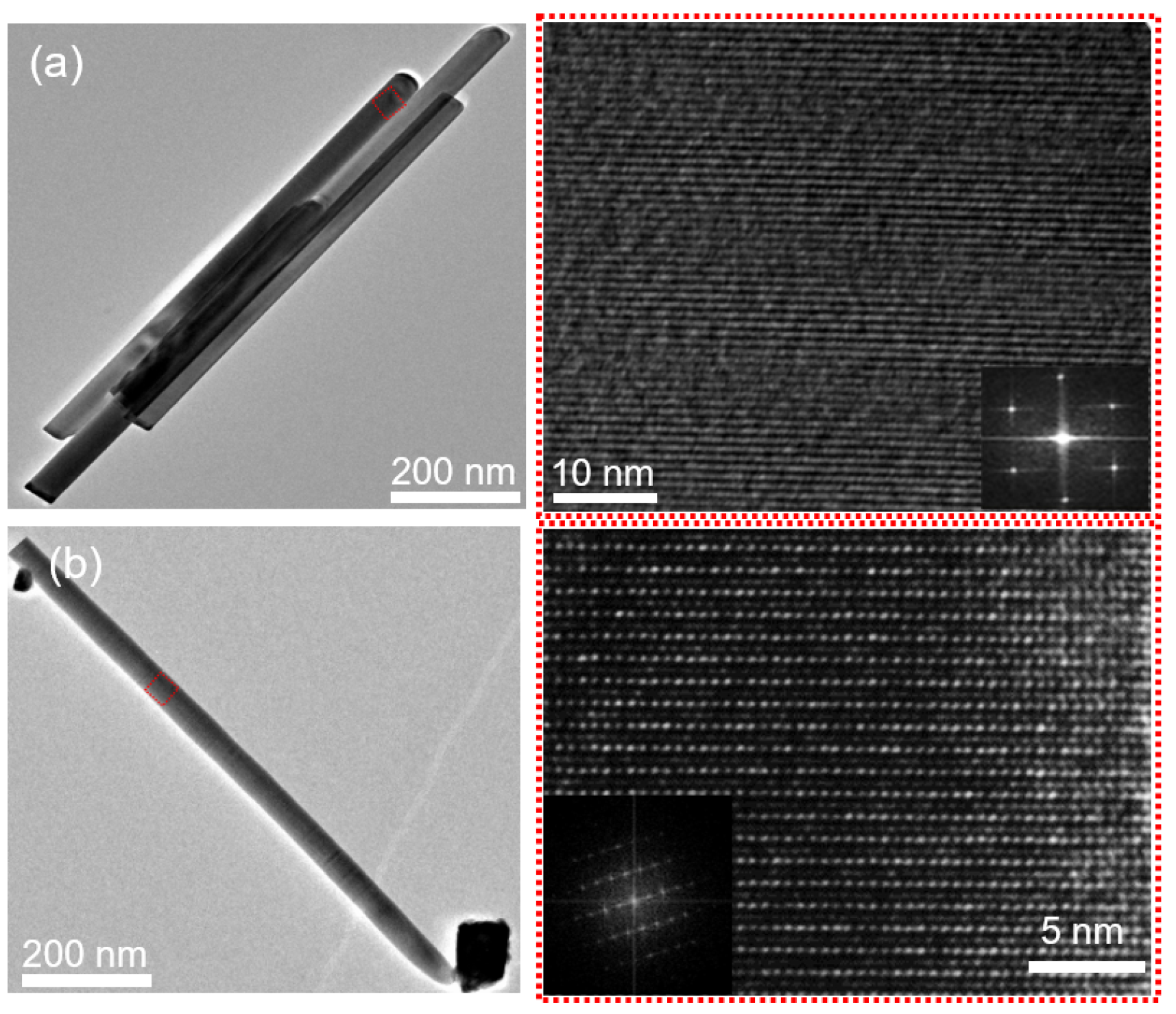
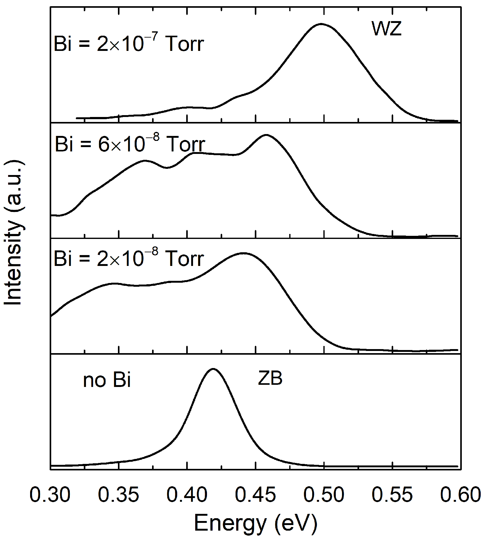
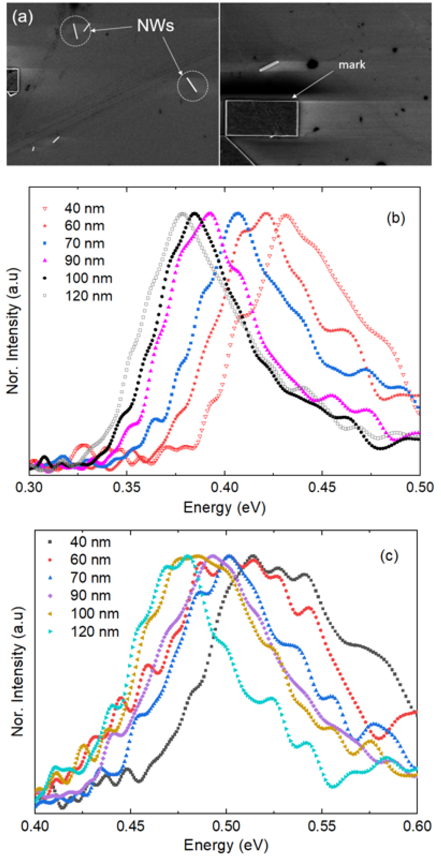
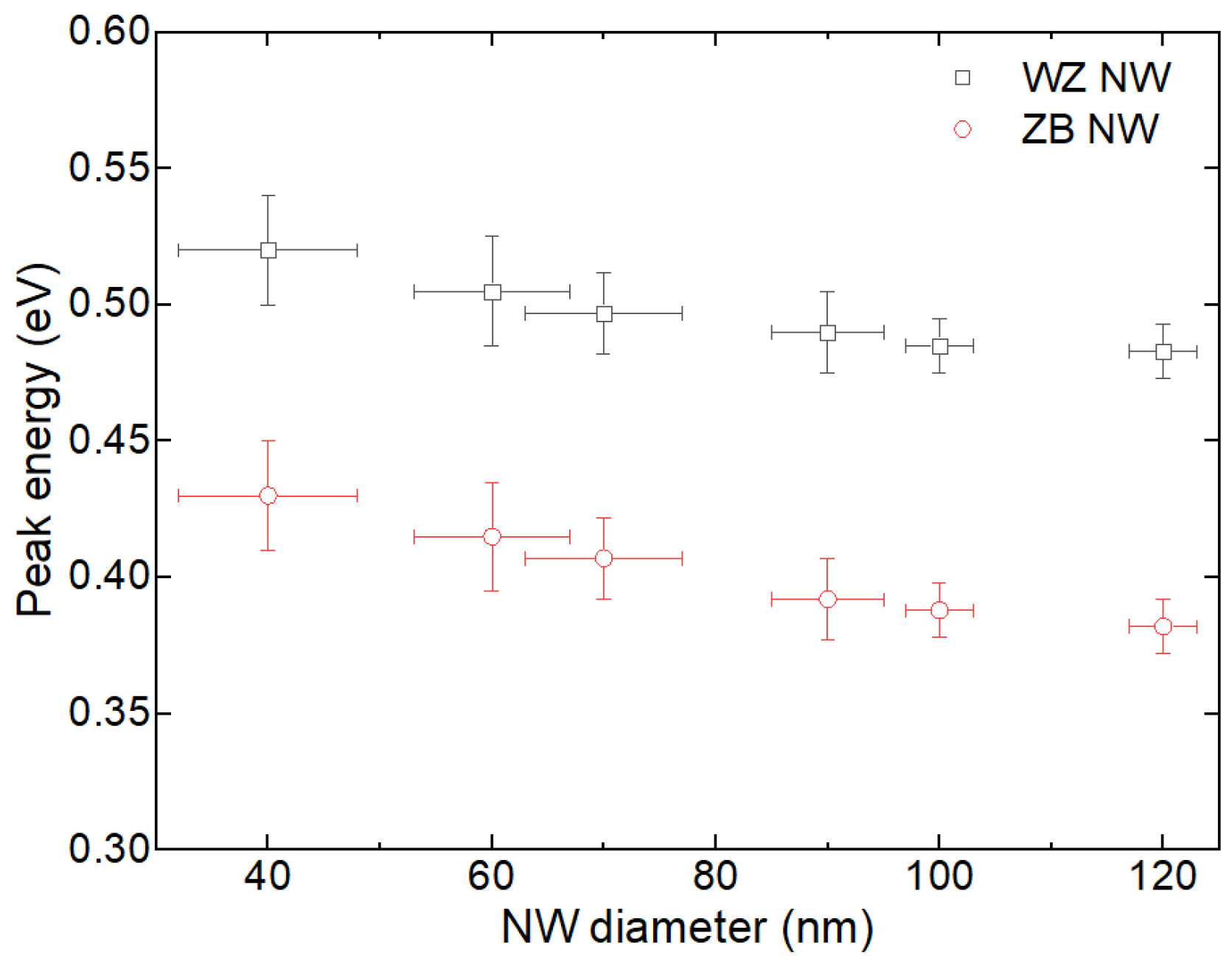
3. Results and Discussion

Figure 1a shows the SEM image of the as-grown InAs NWs without Bi surfactant. InAs NWs are grown along the <111> direction normal to the Si(111) substrate with { 110 } side facets. The average NW length is about 2 μ m and their diameter varies from 40 nm to 120 nm. Figure 1b shows the top view of the WZ phase InAs NWs lying on the sample surface. The InAs NWs with WZ phase were grown using Bi surfactant with Bi-BEP set at 2 × 10 7 Torr. The NWs were intentionally laid down by creating a scratch on the sample surface, with the aim to analyze the NW side wall facets as there was the possibility of the presence of Bi droplets on the NWs as reported previously for GaAsBi NW growth [22]. It can be seen that no Bi droplets are present on the NW side facets.
Figure 2 shows the TEM image and selective area diffraction pattern of the fraction of NW diameter. Figure 2a confirms that the NWs were grown epitaxially along <111> and the selective area diffraction pattern of InAs NWs indicates that the NWs exhibited a ZB crystal structure with side facets along [11 2 ¯ ] directions. No planar crystallographic defects were observed. Figure 2b shows the NWs with WZ crystal structure grown along the c-axis and displays side facets along the { 1 ¯ 100 } direction. In order to understand the WZ crystal growth, it is necessary to consider the growth kinetics.
It is commonly accepted that III-As compound semiconductor WZ crystal phases have lower surface energy than the ZB crystal phase. Studies suggested that InAs WZ crystal phase growth can be promoted if the growth happens under supersaturation conditions with an In-rich environment. In addition, this can occur if the growth conditions are thermodynamically favorable for large WZ phase nucleation which is possible only when the critical radius and nucleation barrier for the WZ phase are smaller than for the ZB phase [15,17]. As proposed earlier, the Bi surfactant lowers the surface energy at the growth plane as well as increases the adatoms diffusion [19]. Lower surface energy and higher diffusion coefficient provoke large WZ phase nucleation, and this explained the clear correlation between the Bi-flux and WZ phase growth.
Figure 3 shows the normalized PL spectra of InAs NWs grown under different Bi-fluxes. Although samples were grown for various Bi-BEPs, here, we only consider those Bi-fluxes which had a strong impact on the NW crystal structure. The PL spectra of pure ZB InAs NWs are shown in the bottom panel as a reference. The peak energy of ZB NWs is at 0.42 eV ( λ ∼ 2900 nm) with 30 meV full-width half-maxima (FWHM). The WZ NW emission spectra are presented in the top panel at the highest Bi-BEP with emission peak energy at 0.505 eV ( λ ∼ 2400 nm) with FWHM of 35 meV. As the PL emission spectra of a material also provide the bandgap energy of the material, from the peak energy we conclude that the WZ InAs NW bandgap energy is 70 to 100 meV higher than the ZB InAs NW bandgap energy. This is similar to findings reported previously [10,14,16,27]. The large FWHM are attributed to band-edge energy indicating PL spectra from NWs of various diameters since the laser spot size is about 10 μ m in diameter. The peak energy emission’s dependence on NW diameter as discussed later in the text.
It can be seen in Figure 3 that when increasing the Bi-flux, the dominant peak in the spectra reveals a blue shift with a sharp decline towards the high-energy edge and an elongated shoulder towards the lower energy side. The broad shoulder indicates the presence of additional peaks. Previous reports indicate that InAs NWs with mixed WZ/ZB phase crystal structures exhibited similar emission spectra [10,18]. As the main peak is at about 0.470 eV with higher intensity, therefore, it can be assumed that the WZ phase contents in the NW crystal structure are dominant and increase when increasing the Bi-BEP.
Here, it is worth mentioning that the optical emission energy of the NWs depends on the crystal structure as well as on the NW diameter due to the possibility of a quantum confinement phenomenon in addition to substrate-induced strain effects [16,28]. In order to explore the diameter-dependent optical properties of InAs NWs, we take full advantage of NWs grown unintentionally with different diameters and intentionally with pure ZB and WZ crystal phase. For this purpose, NWs were mechanically transferred onto a patterned Si/ SiO 2 substrate as shown in Figure 4a. A set of different diameter NWs were selected and located for micro-PL analysis. Figure 4b,c show the emission spectra of ZB and WZ NWs with diameters varying from 40 nm to 120 nm. A clear blue shift can be observed with the decreasing diameter of NWs, for both ZB and WZ phase NWs. It can be seen that ZB NWs showed a 50 meV peak shift while WZ NWs showed a 35 meV peak energy shift with decreasing NW diameter. Kobmuller et al. also found a similar blue shift in the peak energy of ZB NW with decreasing NW diameter [28].
Figure 5 shows the peak emission energy versus NW diameter. The peak energy shows a weak dependence on the NW diameter in the range of 80 nm to 120 nm and the observed change in energy can be attributed to built-in strain, since NWs were grown on Si substrate which has a different lattice constant as compared to InAs. Such peak energy changes have been observed previously for InAs NWs grown on Si substrate [16]. However, a strong dependence of the peak energy on the NW diameter in the range of 40 nm and 60 nm can be observed and is attributed to a quantum confinement effect which cannot be completely ruled out since the Bohr radius of ZB InAs is ∼35 nm and for WZ InAs it is ∼39 nm [10,28]. The error bars in Figure 5 represent the uncertainty in the measured NW diameter and the extracted peak energy which decreases with the increasing diameter of the NWs. Moreover, a peak broadening with the decreasing diameter of NWs can also be observed in Figure 4b,c. It is a known fact that InAs is a degenerate semiconductor and is intrinsically n-type doped. Therefore, the observed peak broadening can be explained by considering the donor-band transitions and donor–acceptor pair transitions that have impurities such as slow recombination rates [10,29].

4. Conclusions

In summary, both WZ and ZB InAs nanowires were successfully grown on Si substrate using Bi surfactant. It is found that there is a correlation between Bi-flux and the percentage of WZ phase contents in the NWs. Furthermore, photoluminescence spectroscopy investigation of both WZ and ZB InAs NWs revealed a peak energy of ∼0.50 eV and ∼0.42 eV, respectively, which is in good agreement with the theoretically estimated bandgap of InAs NWs. Our findings also showed the possibility to grow mixed crystal phases by controlling the Bi-flux which may apply to bandgap engineering within NWs for the mid-infrared range. It is also believed that the interesting finding regarding the use of Bi as a surfactant would instigate future studies, especially to understand the influence of Bi as a surfactant on growth kinetics and phase control growth of III-As materials.

Author Contributions

Conceptualization, S.S. and M.A.; methodology, S.S.; validation, M.A., A.M. and K.F.; formal analysis, S.S. and A.M.; investigation, S.S.; resources, M.A. and H.N.; data validation, K.F.; writing—original draft preparation, S.S.; writing—review and editing, S.S., A.M., K.F., M.A., H.N. and F.J.; visualization, S.S.; supervision, M.A.; project administration, M.A.; funding acquisition, M.A. All authors have read and agreed to the published version of the manuscript.

Funding

This research received no external funding.

Institutional Review Board Statement

Not applicable.

Informed Consent Statement

Not applicable.

Data Availability Statement

Data is contained within the article.

Conflicts of Interest

The authors declare no conflict of interest.

References

  1. Yang, P.; Yan, R.; Fardy, M. Semiconductor nanowire: What’s next? Nano Lett. 2010, 10, 1529–1536. [Google Scholar] [CrossRef] [PubMed]
  2. Tomioka, K.; Motohisa, J.; Hara, S.; Fukui, T. Control of InAs nanowire growth directions on Si. Nano Lett. 2008, 8, 3475–3480. [Google Scholar] [CrossRef] [PubMed]
  3. Offermans, P.; Crego-Calama, M.; Brongersma, S.H. Gas detection with vertical InAs nanowire arrays. Nano Lett. 2010, 10, 2412–2415. [Google Scholar] [CrossRef] [PubMed]
  4. Mingo, N. Thermoelectric figure of merit and maximum power factor in III-V semiconductor nanowires. Appl. Phys. Lett. 2004, 84, 2652–2654. [Google Scholar] [CrossRef]
  5. Koskinen, T.; Khayrudinov, V.; Emadi, F.; Jiang, H.; Haggren, T.; Lipsanen, H.; Tittonen, I. Thermoelectric Characteristics of InAs Nanowire Networks Directly Grown on Flexible Plastic Substrates. ACS Appl. Energy Mater. 2021, 4, 14727–14734. [Google Scholar] [CrossRef]
  6. Wang, L.; Zhang, L.; Yue, L.; Liang, D.; Chen, X.; Li, Y.; Lu, P.; Shao, J.; Wang, S. Novel dilute bismide, epitaxy, physical properties and device application. Crystals 2017, 7, 63. [Google Scholar] [CrossRef]
  7. Töpfer, T.; Petrov, K.P.; Mine, Y.; Jundt, D.; Curl, R.F.; Tittel, F.K. Room-temperature mid-infrared laser sensor for trace gas detection. Appl. Opt. 1997, 36, 8042–8049. [Google Scholar] [CrossRef]
  8. Du, J.; Liang, D.; Tang, H.; Gao, X.P. InAs nanowire transistors as gas sensor and the response mechanism. Nano Lett. 2009, 9, 4348–4351. [Google Scholar] [CrossRef]
  9. Muhiyudin, M.; Hutson, D.; Gibson, D.; Waddell, E.; Song, S.; Ahmadzadeh, S. Miniaturised Infrared Spectrophotometer for Low Power Consumption Multi-Gas Sensing. Sensors 2020, 20, 3843. [Google Scholar] [CrossRef]
  10. Sun, M.; Leong, E.; Chin, A.; Ning, C.Z.; Cirlin, G.; Samsonenko, Y.B.; Dubrovskii, V.; Chuang, L.; Chang-Hasnain, C. Photoluminescence properties of InAs nanowires grown on GaAs and Si substrates. Nanotechnology 2010, 21, 335705. [Google Scholar] [CrossRef]
  11. Sumikura, H.; Zhang, G.; Takiguchi, M.; Takemura, N.; Shinya, A.; Gotoh, H.; Notomi, M. Mid-infrared lasing of single wurtzite InAs nanowire. Nano Lett. 2019, 19, 8059–8065. [Google Scholar] [CrossRef] [PubMed]
  12. Joyce, H.J.; Wong-Leung, J.; Gao, Q.; Tan, H.H.; Jagadish, C. Phase perfection in zinc blende and wurtzite III-V nanowires using basic growth parameters. Nano Lett. 2010, 10, 908–915. [Google Scholar] [CrossRef] [PubMed]
  13. Dayeh, S.A.; Susac, D.; Kavanagh, K.L.; Yu, E.T.; Wang, D. Structural and Room-Temperature Transport Properties of Zinc Blende and Wurtzite InAs Nanowires. Adv. Funct. Mater. 2009, 19, 2102–2108. [Google Scholar] [CrossRef]
  14. Koblmüller, G.; Hertenberger, S.; Vizbaras, K.; Bichler, M.; Bao, F.; Zhang, J.; Abstreiter, G. Self-induced growth of vertical free-standing InAs nanowires on Si (111) by molecular beam epitaxy. Nanotechnology 2010, 21, 365602. [Google Scholar] [CrossRef]
  15. Johansson, J.; Dick, K.A.; Caroff, P.; Messing, M.E.; Bolinsson, J.; Deppert, K.; Samuelson, L. Diameter dependence of the wurtzite- zinc blende transition in InAs nanowires. J. Phys. Chem. C 2010, 114, 3837–3842. [Google Scholar] [CrossRef]
  16. Rota, M.B.; Ameruddin, A.S.; Fonseka, H.A.; Gao, Q.; Mura, F.; Polimeni, A.; Miriametro, A.; Tan, H.H.; Jagadish, C.; Capizzi, M. Bandgap energy of wurtzite InAs nanowires. Nano Lett. 2016, 16, 5197–5203. [Google Scholar] [CrossRef]
  17. Biermanns, A.; Dimakis, E.; Davydok, A.; Sasaki, T.; Geelhaar, L.; Takahasi, M.; Pietsch, U. Role of liquid indium in the structural purity of wurtzite InAs nanowires that grow on Si (111). Nano Lett. 2014, 14, 6878–6883. [Google Scholar] [CrossRef]
  18. Möller, M.; de Lima, M., Jr.; Cantarero, A.; Chiaramonte, T.; Cotta, M.; Iikawa, F. Optical emission of InAs nanowires. Nanotechnology 2012, 23, 375704. [Google Scholar] [CrossRef]
  19. Tixier, S.; Adamcyk, M.; Young, E.; Schmid, J.; Tiedje, T. Surfactant enhanced growth of GaNAs and InGaNAs using bismuth. J. Cryst. Growth 2003, 251, 449–454. [Google Scholar] [CrossRef]
  20. Lewis, R.B.; Corfdir, P.; Li, H.; Herranz, J.; Pfüller, C.; Brandt, O.; Geelhaar, L. Quantum dot self-assembly driven by a surfactant-induced morphological instability. Phys. Rev. Lett. 2017, 119, 086101. [Google Scholar] [CrossRef] [Green Version]
  21. Lu, Z.; Zhang, Z.; Chen, P.; Shi, S.; Yao, L.; Zhou, C.; Zhou, X.; Zou, J.; Lu, W. Bismuth-induced phase control of GaAs nanowires grown by molecular beam epitaxy. Appl. Phys. Lett. 2014, 105, 162102. [Google Scholar] [CrossRef] [Green Version]
  22. Ishikawa, F.; Akamatsu, Y.; Watanabe, K.; Uesugi, F.; Asahina, S.; Jahn, U.; Shimomura, S. Metamorphic GaAs/GaAsBi heterostructured nanowires. Nano Lett. 2015, 15, 7265–7272. [Google Scholar] [CrossRef] [PubMed]
  23. Fan, D.; Zeng, Z.; Dorogan, V.G.; Hirono, Y.; Li, C.; Mazur, Y.I.; Yu, S.Q.; Johnson, S.R.; Wang, Z.M.; Salamo, G.J. Bismuth surfactant mediated growth of InAs quantum dots by molecular beam epitaxy. J. Mater. Sci. Mater. Electron. 2013, 24, 1635–1639. [Google Scholar] [CrossRef]
  24. Wang, L.; Pan, W.; Chen, X.; Wu, X.; Shao, J.; Wang, S. Influence of Bi on morphology and optical properties of InAs QDs. Opt. Mater. Express 2017, 7, 4249–4257. [Google Scholar] [CrossRef]
  25. Webster, P.T.; Schaefer, S.T.; Steenbergen, E.H.; Johnson, S.R. Optical quality in strain-balanced InAs/InAsSb superlattices grown with and without Bi surfactant. In Proceedings of the Quantum Sensing and Nano Electronics and Photonics XV. International Society for Optics and Photonics, San Francisco, CA, USA, 28 January–2 February 2018; Volume 10540, p. 105401E. [Google Scholar]
  26. Alghamdi, H.; Alhassni, A.; Alhassan, S.; Almunyif, A.; Klekovkin, A.V.; Trunkin, I.N.; Vasiliev, A.L.; Galeti, H.V.; Gobato, Y.G.; Kazakov, I.P.; et al. Effect of bismuth surfactant on the structural, morphological and optical properties of self-assembled InGaAs quantum dots grown by Molecular Beam Epitaxy on GaAs (001) substrates. J. Alloys Compd. 2022, 164015. [Google Scholar] [CrossRef]
  27. Bao, J.; Bell, D.C.; Capasso, F.; Erdman, N.; Wei, D.; Fröberg, L.; Mårtensson, T.; Samuelson, L. Nanowire-Induced Wurtzite InAs Thin Film on Zinc-Blende InAs Substrate. Adv. Mater. 2009, 21, 3654–3658. [Google Scholar] [CrossRef]
  28. Koblmüller, G.; Vizbaras, K.; Hertenberger, S.; Bolte, S.; Rudolph, D.; Becker, J.; Döblinger, M.; Amann, M.C.; Finley, J.; Abstreiter, G. Diameter dependent optical emission properties of InAs nanowires grown on Si. Appl. Phys. Lett. 2012, 101, 053103. [Google Scholar] [CrossRef]
  29. Sun, M.; Joyce, H.J.; Gao, Q.; Tan, H.; Jagadish, C.; Ning, C.Z. Removal of surface states and recovery of band-edge emission in InAs nanowires through surface passivation. Nano Lett. 2012, 12, 3378–3384. [Google Scholar] [CrossRef] [Green Version]
Figure 1. SEM micrograph of catalyst-free selective area InAs nanowires, (a) top view (inset) and 30 tilted view of zincblende nanowires, (b) top view (inset) of as-grown and mechanically placed wurtzite InAs nanowires on Si substrate for surface analysis.
Coatings 12 00250 g001
Figure 2. High-resolution TEM image of pure (a) zincblende and (b) wurtzite InAs nanowires.
Coatings 12 00250 g002
Figure 3. Photoluminescence emission spectra of InAs NWs taken at 8 K with different Bi-fluxes. Bi-flux varies from 2 × 10 8 Torr to 2 × 10 7 Torr. Bottom panel of the figure is the reference sample with zero Bi-flux, indicating ZB nanowire energy bandgap, and the top panel shows highest Bi-flux and WZ energy bandgap.
Coatings 12 00250 g003
Figure 4. (a) SEM micrographs of the InAs nanowires transferred onto a marked Si/ SiO 2 substrate. Photoluminescence spectra of different diameter nanowires taken at 8 K, (b) zincblende (c) wurtzite.
Coatings 12 00250 g004
Figure 5. Peak energy shift of the spectra in Figure 4 versus nanowire diameter. Error bars represent the uncertainty in the measured NW diameter and the peak energy.
Coatings 12 00250 g005
Publisher’s Note: MDPI stays neutral with regard to jurisdictional claims in published maps and institutional affiliations.

