Article

Effect of Substrate Temperature on the Properties of RF Magnetron Sputtered p-CuInOx Thin Films for Transparent Heterojunction Devices

Department of Electrical and Computer Engineering, University of Central Florida, Orlando, FL 32816, USA
*
Author to whom correspondence should be addressed.
Coatings 2022, 12(4), 500; https://doi.org/10.3390/coatings12040500
Submission received: 8 March 2022 / Revised: 29 March 2022 / Accepted: 6 April 2022 / Published: 8 April 2022
(This article belongs to the Special Issue Recent Advances in the Growth and Characterizations of Thin Films)

Abstract

:
Copper indium oxide (CuInOx) thin films were deposited by the RF magnetron sputtering technique using a Cu2O:In2O3 target at varying substrate temperatures up to 400 °C. Mutually exclusive requirements of having a p-type thin film along with increased conductivity and high transparency were achieved by controlling the migration of indium oxide phases during the sputtering process, as verified by the XPS studies. A morphological study performed using SEM further confirmed the crystallization and the grain growth (95–135 nm) with increasing substrate temperatures, resulting in superior conductivity and an enhanced transparency of more than 70% in the 400–700 nm range. This is due to the controlled replacement of copper sites with indium while maintaining the p-type characteristic of the thin film. Optical studies carried out on the films indicated a bandgap change in the range of 2.46–2.99 eV as a function of substrate heating. A p-CuInOx/n-Si heterojunction was fabricated with a measured knee voltage of 0.85 V. The photovoltaic behavior of the device was investigated and initial solar cell parameters are reported.

1. Introduction

Transparent conducting oxides (TCOs) have unique optoelectronic properties which allow visible light to pass through while having reasonably high electrical conductivity [1,2,3]. TCOs have a variety of applications ranging from uses in solar cells, optical displays, reflective coatings, light emission devices, low-emissivity windows, electrochromic mirrors, UV sensors, and windows, defrosting windows, electromagnetic shielding, and transparent electronics [4,5]. The conductivity of TCOs can be tuned from insulating via semiconducting to conducting. Their transparency can also be adjusted depending on the donor/acceptor levels as well as the bandgap of the material. This enables the realization of both n-type and p-type TCOs, which make them highly attractive for transparent opto-electrical circuitries and technological applications. Most research activities have focused on the optimization of n-type TCOs [6,7,8,9], but many transparent electronic applications require the necessity of p-type TCOs as well.
Various techniques have been proposed to obtain p-TCO thin films with better electrical and optical properties. In spite of that, the conductivity of p-TCO thin films is still one or two orders of magnitude less than that in the corresponding n-TCO thin films. Increasing the conductivity of p-TCO thin films without sacrificing their visible transmittance is the most significant challenge for p-TCO technology in order to obtain high-performance active devices suitable for ‘‘Invisible Electronics’’ [10]. It may be noted that p-type transparent oxide semiconductors based on CuAlO2, CuGaO2, CuInO2, SrCu2O2, and LaCuOCh (Ch = chalcogen) have been reported [11]. Copper indium oxide–copper aluminum oxide and copper gallium oxide-based thin-film materials have emerged as the front runner for possible p-type TCO applications [10,11,12,13]. Of the copper-based systems, the CuInO2 system is particularly interesting because it can be doped with both p-type (with Ca) and n-type (with Sn), allowing p–n homojunctions to be produced. The synthesis of Cu2In2O5 has been reported only using either smelting [14] or chemical processes, which involve synthesizing Cu2In2O5 from aqueous solutions of nitrates, chlorides, and sulfates of Cu, In, and Ga [15]. Therefore, the realization of p-type TCOs has been rather challenging and involves the use of chemicals that present levels of toxicity and low yield or smelting which results in a high thermal budget for the fabricated device.
However, recently, Nair et al. fabricated a transparent thin-film p–n junction consisting of Ca and tin-doped CuInO2 [16] by oxygen plasma-enhanced reactive thermal evaporation. This allows for the scalable physical vapor phase deposition of the desired thin films. [10] Thus, there is a need to realize p-type TCOs which offer high yield, scalability, and low cost. RF magnetron sputtering of TCO sources, if controlled in situ, can lead to high uniformity and homogeneity, along with the ability to control the film thickness and deposition rate. It also allows for large-area deposition at a relatively low cost and optimum thermal budget [7,12,13,17,18,19].
In this work, we investigate the realization of p-type CuInOx thin films by RF magnetron sputtering and study the effects of substrate heating for the in situ controlling of the optoelectronic and morphological properties. It is seen that substrate heating influences the material characteristics more significantly than post-deposition annealing [13]. We can tailor the thin-film characteristics in situ to initiate crystalline growth and control the proportion of indium oxide or copper oxide phases to improve the transparency while retaining the p-type characteristics of the thin film at a reduced thermal budget as compared with post-deposition annealing [13]. Scanning electron microscopy imaging has been used to obtain the grain size of the film and UV-Vis spectral measurements have been carried out for transmittance studies. XPS analysis of the thin films has also been carried out to identify the oxidation state and bonding configurations of Cu, In, and O in copper indium oxide films. Junction studies of the p-type CuInOx have been investigated with n-Si and ITO for demonstrating heterojunction behavior, which can potentially find applications in transparent electronics, photodetectors, and solar cells.

2. Experimental Details

2.1. Deposition of Copper Indium Oxide Thin Films with Substrate Heating

Thin films of copper indium oxide (CuInOx) were deposited using radio frequency (RF) magnetron sputtering. MAK 2 sputter gun (San Jose, CA, USA) was driven by a Dressler Cesar 136 FST RF Generator (Denver, CO, USA) and an Advanced Energy VarioMatch-1000 matching network (Fort Collins, CO, USA). The deposition pressure was 10 mTorr, having an argon (Ar) flow of 10 sccm. All the depositions were performed at a power of 100 W on silicon/quartz substrates. The deposition pressure, argon flow and deposition power were chosen based on the optimal deposition rate during the sputtering process. Acetone and methanol were used to clean the substrates and they were rinsed with deionized water and blow dried with a nitrogen gun prior to the deposition.
A 2” powder-pressed target of Cu2O/In2O3 (1/1 mol%, 99.9% purity), ACI Alloy Inc. (San Jose, CA, USA), was used as a sputtering target. Highly dense single-phase targets for CuInO2 thin-film growing are still challenging, therefore a Cu2O–In2O3 composite target instead of a CuInO2 single-phase target was used in this study. Furthermore, having the composite target allows for more flexibility in controlling the Cu2O and In2O3 phases in the deposited thin film. The target and the substrate separation was maintained at 5 cm to achieve a uniform film thickness. Base pressure of 5 × 10⁻⁶ Torr was achieved before initiating the deposition. The deposition rate was measured for varying substrate temperatures. The thickness was measured using a Veeco Dektak-150 profilometer (Plainview, NY, USA). All films were deposited with a thickness of 2000 Å at the different substrate temperatures.

2.2. Morphological and Optical Studies of Copper Indium Oxide Thin Films

A field emission scanning electron microscope, Zeiss ULTRA-55 FEG SEM (Zeiss Microscopy, White Plains, NY, USA), was used for morphological studies. An acceleration voltage of 5 kV was used for the imaging at a working distance of 0.2 mm. A Cary 100 UV–Vis spectrophotometer (Varian Analytical Instruments, Walnut Creek, CA, USA) was used to measure the transmittance for a wavelength range of 300–800 nm. The composition of the films was determined using ESCALAB 250 Xi + X-ray photoelectron spectroscopy (XPS) by Thermo Fisher Scientific with a monochromatic Al Kα source (1486.7 eV). To remove the surface oxygen, a monatomic EX06 ion source (4 kV) was used to perform ion milling of the film surface for 30 s prior to the measurements. Thermo Fisher Scientific Avantage (software version 5.9902) was used to identify the elemental composition and fit the XPS peaks. A smart Shirley function was used to subtract the background for the XPS spectra. The peak fitting was performed by using a mixed Gaussian function after background subtraction.

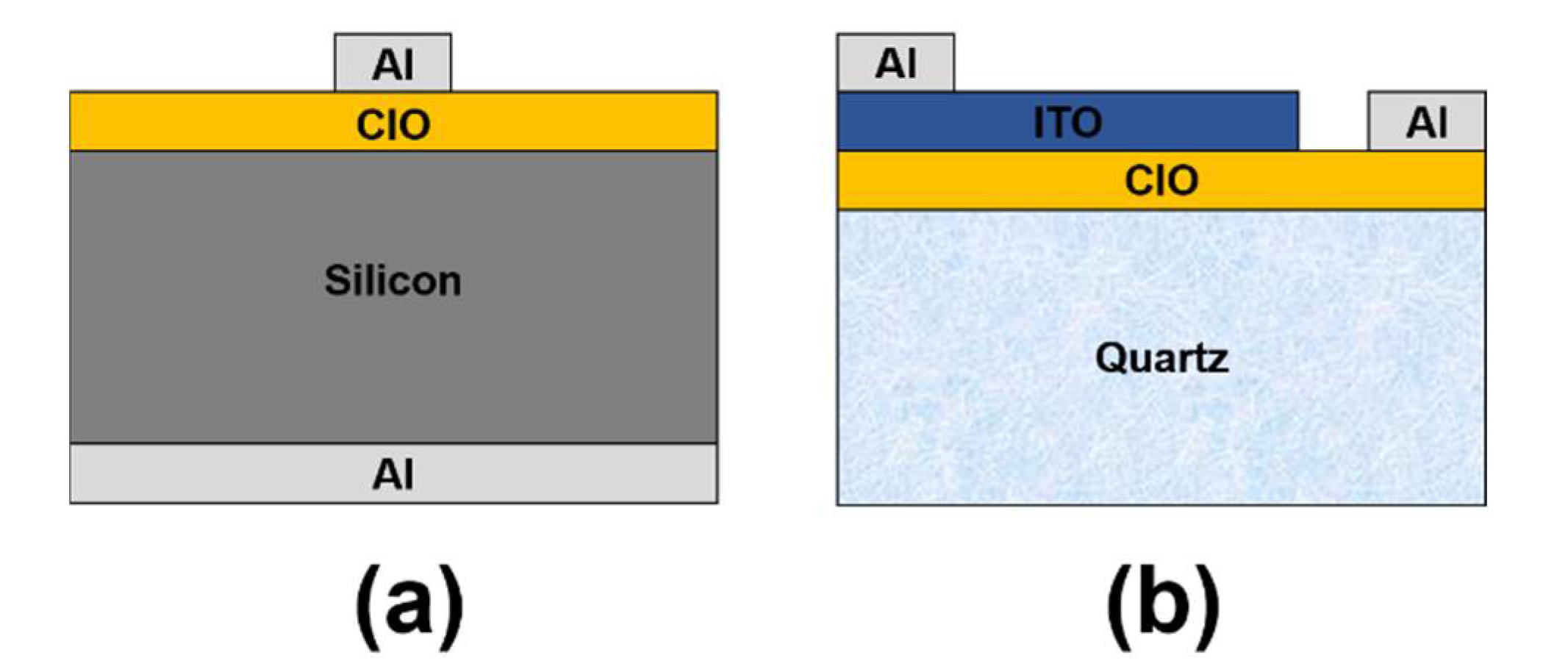
2.3. Fabrication of CuInOx Heterojunctions and Electrical Studies

(a) The 1–20 Ω-cm n-type silicon was used to fabricate the Si heterojunctions. Aluminum, as the contact for the n-type silicon, was deposited on the backside of the silicon using the thermal evaporation technique. Post annealing at 400 °C for 30 min in N2 ambiance was conducted before depositing the CuInOx thin films. Figure 1a shows the structure of the fabricated device.
(b) A quartz substrate was used to fabricate the heterojunction on a transparent platform. In total, 4000 Å of copper indium oxide films were deposited with a substrate temperature of 400 °C. A 1 cm × 1 cm area was opened and the rest of the area was masked using aluminum foil, and indium tin oxide was deposited by RF magnetron sputtering (100 W, 10 mTorr, 10 sccm Ar) at room temperature (RT) to obtain a thickness of 4000 Å. A mask with several holes (1 mm diameter) was used to deposit aluminum contacts on copper indium oxide (p-type) as well as indium tin oxide (n-type). Figure 1b shows the structure of the fabricated device.

3. Results and Discussions

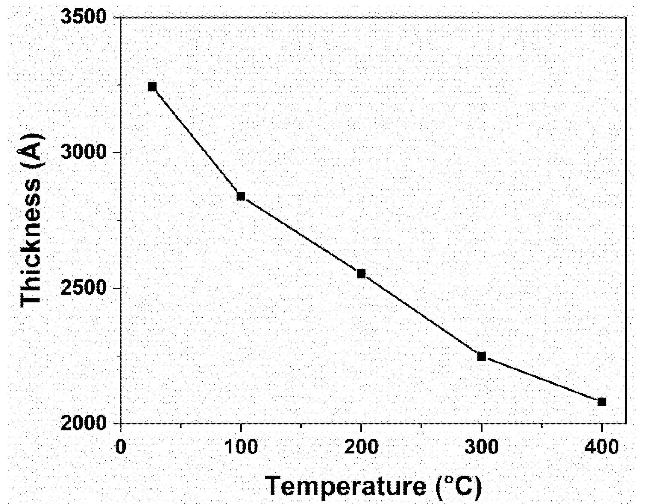
3.1. Deposition and Morphological Studies
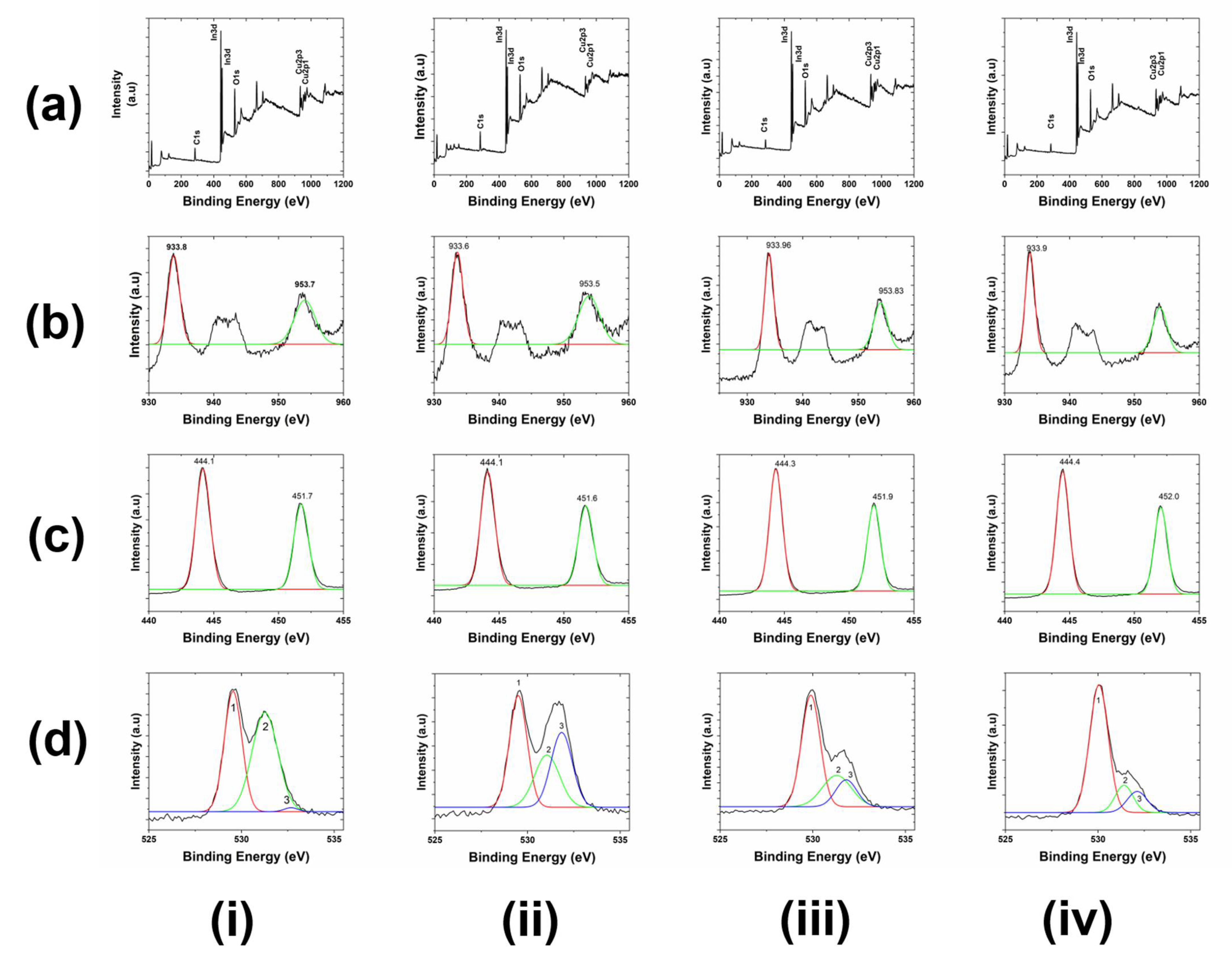
Figure 2 shows the thickness of the obtained films after 5 min of deposition at varying substrate temperatures. It is seen that the final thickness obtained at higher temperatures reduces, which may be attributed to higher thin-film densities and lower porosities [6]. It is interesting to point out here that the substrate temperature also increases due to collisions from secondary electrons [20].
Figure 3 shows the SEM images of as-deposited CIO thin films as well as those obtained at substrate temperatures of 200, 300, and 400 °C. Changes in the morphology were identified as the substrate heating temperature was increased. Films with a substrate deposition temperature of 200 °C displayed the presence of very small grains, as shown in Figure 3b with respect to the film deposited at room temperature. Thus, a minimum of 300–400 °C is required to initiate nanocrystalline growth, as evidenced in the figure. The grain size of 10–30 nm was obtained for the films deposited at 300–400 °C. It is worthy to note that the crystallization occurs at a much lower temperature as compared with post-deposition annealing, which is typically at 500 °C and above. Therefore, a significant reduction in thermal budget is achieved by the process of substrate heating during the RF magnetron sputtering process.

3.2. XPS Analysis

Figure 4a(i–iv) shows the XPS spectra obtained from the CuInOx films sputtered at room temperature, 200, 300, and 400 °C, respectively. Peaks pertaining to Cu, In, and O were identified in the obtained XPS survey spectra shown in Figure 4a(i–iv), confirming the phase purity. From Figure 4b(i–iv), two strong peaks are obtained at 933.8 eV and 953.7 eV, belonging to Cu 2p3/2 and Cu 2p1/2, respectively [21]. The presence of Cu2+ species was confirmed by the satellite peaks between 940 and 950 eV. Figure 4c(i–iv) shows the 3d5/2 and 3d3/2 indium core levels at a binding energy of 444.1 and 451.7 eV [21]. Oxygen 1 s core level, Figure 4d(i–iv), was fitted with three Gaussian peaks located at 529.5, 531.3, and 532.5 eV (marked 1, 2, and 3), respectively. Peak 1 is attributed to oxygen attached to In (+3) while peak 2 is attributed to oxygen attached to Cu (+1). Peak 3 is attributed to strongly chemisorbed oxygen which is normally observed at 532.2 eV [21]. It is seen from Figure 4d(i–iv) that the strength of peak 2 reduces relative to that of peak 1. This indicates that there is a controlled addition of indium oxide phases to the thin film as a result of substrate heating while maintaining sufficient copper oxide phases. The addition of the indium oxide phases causes the thin film to become more transparent while the optimal presence of copper oxide phases enables the film to retain its p-type characteristics. This relative addition of indium oxide phases is due to the loss in the copper oxide phases due to the possible desorption of copper oxide at elevated temperatures. The ratio of the area of the peaks corresponding to indium oxide and copper oxide was performed for room temperature, 200, 300, and 400 °C. It is seen that the ratio of In2O3:Cu2O increases as 0.98, 1.02, 1.06, and 1.11 with respective substrate temperatures corresponding to room temperature, 200, 300, and 400 °C. This is also validated by the transmittance measurements for transparency as well as hot probe measurements for the p-type behavior [18].

3.3. Optical Analysis and Bandgap

Figure 5 shows the percentage transmission for the films deposited on quartz substrates at room temperature, 200, 300, and 400 °C. Overall, the optical transmission increases for the films deposited at higher temperatures. This is because of the controlled relative increase in the indium oxide phases at the copper oxide sites as already verified by the XPS analysis. It is seen that the percentage increase in transmittance varies up to 25%–100% between wavelengths of 400 and 700 nm for a substrate temperature of 400 °C, which may be attributed to the higher transmission of indium oxide over that of copper oxide as the relative concentration of indium oxide increases with an increase in substrate temperature.
The optical bandgap of CuInOx thin films were calculated using the Tauc plot method [22,23] based on the optical transmission data. The absorption coefficient α was calculated directly from the transmission data as the reflectance was less than 5%. Absorption coefficient α was calculated using Equation (1), where d is the thickness of the film equal to 200 nm, and T is the percent of transmission. The optical bandgap (Eg) was estimated from Equation (2),
α = 1 d   ln ( 1 T )
( α h v ) 1 / n = B   ( hv Eg )
where hν is the photon energy, B is a constant, Eg is the optical bandgap, and n = 1/2 for the direct bandgap transition [21]. As demonstrated by Singh et al. [21], the best linear fit in the optical absorption region to the (αhν)1/n versus energy curves were obtained for n = 1/2, implying our thin-film material has a direct band gap. Figure 6 shows the generated Tauc plot. The linear region of the curve was extrapolated to the x-axis to identify the Eg value. The extrapolated values of the bandgap are listed in Figure 6. The bandgap was in the range of 2.46–2.99 eV for temperatures ranging from room temperature to 400 °C (Figure 6). It is worth mentioning that an increase in the bandgap with temperature is also attributed to the relative increase in the indium oxide phases as it has a higher bandgap than copper oxide.

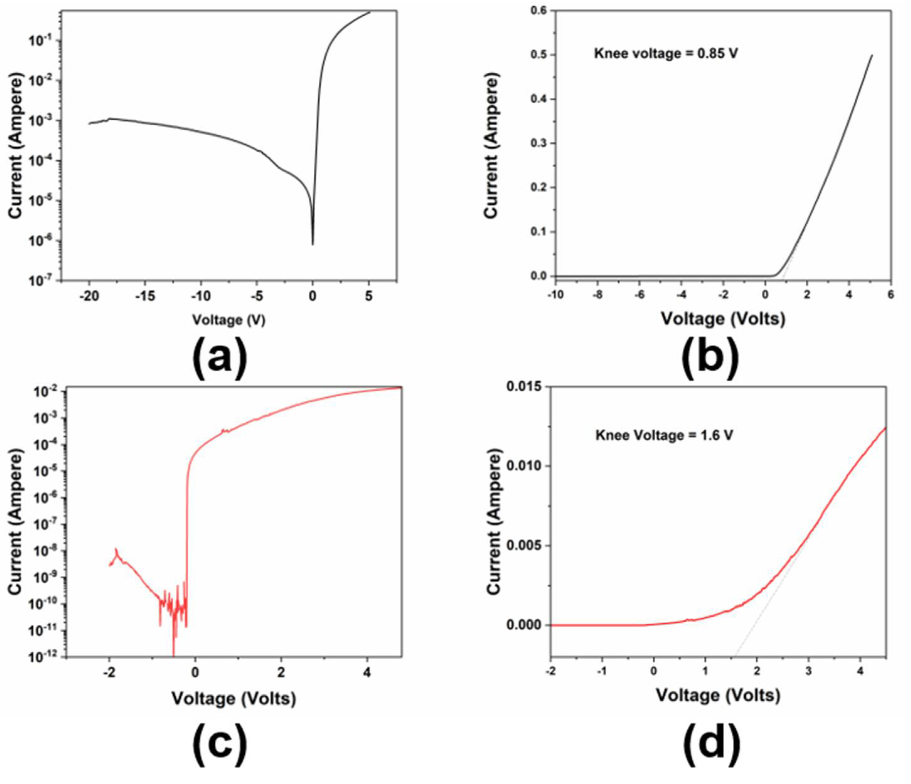
3.4. Electrical Studies

For the fabricated device structures, as outlined in Section 2.3, the I-V characteristics were performed. All the films were deposited at 400 °C as the films deposited at 400 °C had the highest transmission and also showed crystalline grains, as evidenced in the SEM images (Figure 3). For the silicon-based device, a knee voltage of 0.85 V was obtained. The value is similar to that of other such heterojunctions reported in the literature [16]. The I-V characteristics are depicted in Figure 7a,b, which shows n-Si/p-CIO heterojunction behavior. Light characteristics were also performed on the device, and an open-circuit voltage (VOC) of 50 mV and short-circuit current (ISC) of 5 µA were obtained. This confirms that the device is suitable for optoelectronic applications including solar cells and photodetectors. Figure 7c,d shows the I-V characteristics for the quartz-based p-CIO/n-ITO heterojunction with a knee voltage of 1.6V which is close to that of similar heterojunction devices [16,24]. The I-V characteristics again confirm a p-CIO/n-ITO heterojunction which has many potential applications in transparent electronics as both the layers have very high transmittance. Figure 8 shows the photomicrograph of the fabricated device on a quartz substrate showing a high transparency.

4. Conclusions

Copper indium oxide (CuInOx) films, having a p-type behavior along with high transparency and superior electrical conductivity, were deposited by RF magnetron sputtering. This control over the electrical, morphological, and optical properties was obtained in situ by varying the substrate temperature during the deposition process. While the p-type nature was controlled by the presence of the copper oxide phases in the deposited thin films, the transparency was controlled by the presence of indium oxide phases. XPS results confirm that at elevated temperatures of 400 °C, the relative increase in indium oxide phases is favored, resulting in a higher optical bandgap of 2.99 eV and better transparency (>45% for 400–700 nm). It may be interesting to note here that further increasing the substrate temperature during the deposition process may increase the transparency further, as well as the crystallization, which may need to be validated by further studies. However, these advantages will be offset by the higher thermal budget with increasing temperature. Optimal optical, electrical, and morphological properties were obtained for depositions carried out at a substrate temperature of 400 °C. The heterojunction behavior of the p-type CIO was confirmed with n-Si and n-ITO, thereby laying the basis for completely transparent TCO-based optoelectronic devices.

Author Contributions

Conceptualization, K.B.S.; Data curation, G.S. and A.K.; Formal analysis, G.S. and A.K.; Investigation, G.S.; Methodology, G.S., A.K. and K.B.S.; Project administration, G.S. and K.B.S.; Software, G.S.; Supervision, K.B.S.; Validation, G.S. and A.K.; Writing—original draft, G.S.; Writing—review & editing, K.B.S. All authors have read and agreed to the published version of the manuscript.

Funding

A portion of the article processing charges were provided by the UCF College of Graduate Studies Open Access Publishing Fund.

Institutional Review Board Statement

Not applicable.

Informed Consent Statement

Not applicable.

Data Availability Statement

Not applicable.

Conflicts of Interest

The authors declare no conflict of interest.

References

  1. Ginley, D.S.; Bright, C. Transparent conducting oxides. MRS Bull. 2000, 25, 15–18. [Google Scholar] [CrossRef]
  2. Fortunato, E.; Ginley, D.; Hosono, H.; Paine, D.C. Transparent conducting oxides for photovoltaics. MRS Bull. 2007, 32, 242–247. [Google Scholar] [CrossRef] [Green Version]
  3. Ye, F.; Cai, X.M.; Dai, F.P.; Zhang, D.P.; Fan, P.; Liu, L.J. Transparent Conductive Cu-In-O Thin Films Deposited by Reactive DC Magnetron Sputtering with Different Targets. In Advanced Materials Research; Trans Tech Publications Ltd.: Kapellweg, Switzerland, 2011. [Google Scholar]
  4. Lewis, B.G.; Paine, D.C. Applications and processing of transparent conducting oxides. MRS Bull. 2000, 25, 22–27. [Google Scholar] [CrossRef]
  5. Szyszka, B.; Loebmann, P.; Georg, A.; May, C.; Elsaesser, C. Development of new transparent conductors and device applications utilizing a multidisciplinary approach. Thin Solid Film. 2010, 518, 3109–3114. [Google Scholar] [CrossRef]
  6. Sundaram, K.; Khan, A. Characterization and optimization of zinc oxide films by rf magnetron sputtering. Thin Solid Film. 1997, 295, 87–91. [Google Scholar] [CrossRef]
  7. Shantheyanda, B.P.; Todi, V.O.; Sundaram, K.B.; Vijayakumar, A.; Oladeji, I. Compositional study of vacuum annealed Al doped ZnO thin films obtained by RF magnetron sputtering. J. Vac. Sci. Technol. A Vac. Surf. Film. 2011, 29, 051514. [Google Scholar] [CrossRef]
  8. Sundaram, K.B.; Bhagavat, G.K. Chemical vapour deposition of tin oxide films and their electrical properties. J. Phys. D Appl. Phys. 1981, 14, 333. [Google Scholar] [CrossRef]
  9. Sundaram, K.B.; Bhagavat, G.K. Low temperature synthesis wide optical band gap Al and (Al, Na) co-doped ZnO thin films. Appl. Surf. Sci. 2011, 257, 2341–2345. [Google Scholar]
  10. Banerjee, A.; Chattopadhyay, K. Recent developments in the emerging field of crystalline p-type transparent conducting oxide thin films. Prog. Cryst. Growth Charact. Mater. 2005, 50, 52–105. [Google Scholar] [CrossRef]
  11. Sheng, S.; Fang, G.; Li, C.; Xu, S.; Zhao, X. p-Type transparent conducting oxides. Phys. Status Solidi 2006, 203, 1891–1900. [Google Scholar] [CrossRef]
  12. Saikumar, A.K.; Sundaresh, S.; Nehate, S.D.; Sundaram, K.B. Properties of RF Magnetron-Sputtered Copper Gallium Oxide (CuGa2O4) Thin Films. Coatings 2021, 11, 921. [Google Scholar] [CrossRef]
  13. Skaria, G.; Kumar Saikumar, A.; Shivprasad, A.D.; Sundaram, K.B. Annealing Studies of Copper Indium Oxide (Cu2In2O5) Thin Films Prepared by RF Magnetron Sputtering. Coatings 2021, 11, 1290. [Google Scholar] [CrossRef]
  14. Su, C.-Y.; Mishra, D.K.; Chiu, C.-Y.; Ting, J.-M. Effects of Cu2S sintering aid on the formation of CuInS2 coatings from single crystal Cu2In2O5 nanoparticles. Surf. Coat. Technol. 2013, 231, 517–520. [Google Scholar] [CrossRef]
  15. Su, C.-Y.; Chiu, C.-Y.; Chang, C.-H.; Ting, J.-M. Synthesis of Cu2In2O5 and CuInGaO4 nanoparticles. Thin Solid Film. 2013, 531, 42–48. [Google Scholar] [CrossRef]
  16. Nair, B.; Rahman, H.; Shaji, S.; Okram, G.; Sharma, V.; Philip, R.R. Calcium incorporated copper indium oxide thin films-a promising candidate for transparent electronic applications. Thin Solid Film. 2020, 693, 137673. [Google Scholar] [CrossRef]
  17. Sundaresh, S.; Nehate, S.D.; Sundaram, K.B. Electrical and optical studies of reactively sputtered indium oxide thin films. ECS J. Solid State Sci. Technol. 2021, 10, 065016. [Google Scholar] [CrossRef]
  18. Saikumar, A.K.; Sundaresh, S.; Nehate, S.D.; Sundaram, K.B. Preparation and Characterization of Radio Frequency Sputtered Delafossite p-type Copper Gallium Oxide (p-CuGaO2) Thin Films. ECS J. Solid State Sci. Technol. 2022, 11, 023005. [Google Scholar] [CrossRef]
  19. Ray, S.; Banerjee, R.; Basu, N.; Batabyal, A.K.; Barua, A.K. Properties of tin doped indium oxide thin films prepared by magnetron sputtering. J. Appl. Phys. 1983, 54, 3497–3501. [Google Scholar] [CrossRef]
  20. Sundaram, K.B.; Garside, B.K. Properties of ZnO films reactively RE sputtered using a Zn target. J. Phys. D Appl. Phys. 1984, 17, 147. [Google Scholar] [CrossRef]
  21. Singh, M.; Singh, V.N.; Mehta, B.R. Synthesis and properties of nanocrystalline copper indium oxide thin films deposited by RF magnetron sputtering. J. Nanosci. Nanotechnol. 2008, 8, 3889–3894. [Google Scholar] [CrossRef]
  22. Ohyama, M.; Kozuka, H.; Yoko, T. Sol-gel preparation of transparent and conductive aluminum-doped zinc oxide films with highly preferential crystal orientation. J. Am. Ceram. Soc. 1998, 81, 1622–1632. [Google Scholar] [CrossRef]
  23. Sundaram, K.B.; Bhagavat, G.K. Optical absorption studies on tin oxide films. J. Phys. D Appl. Phys. 1981, 14, 921. [Google Scholar] [CrossRef]
  24. Yanagi, H.; Ueda, K.; Ohta, H.; Orita, M.; Hirano, M.; Hosono, H. Fabrication of all oxide transparent p–n homojunction using bipolar CuInO2 semiconducting oxide with delafossite structure. Solid State Commun. 2001, 121, 15–17. [Google Scholar] [CrossRef]
Figure 1. Device schematic for (a) n-Si/p-CIO heterojunction and (b) quartz p-CIO/n-ITO heterojunction.
Coatings 12 00500 g001
Figure 2. Thickness of CuInOx films at varying substrate temperatures after 5 min of sputtering process.
Coatings 12 00500 g002
Figure 3. SEM images of CuInOx films on quartz: (a) room temperature, (b) substrate temperature of 200 °C, (c) substrate temperature of 300 °C, (d) substrate temperature of 400 °C.
Coatings 12 00500 g003
Figure 4. (a) XPS spectra of CuInOx thin films with (b) copper peaks, (c) indium peaks, and (d) oxygen peaks. (iiv) correspond to room temperature, 200 °C, 300 °C, and 400 °C, respectively.
Coatings 12 00500 g004
Figure 5. (a) Transmittance spectra of CuInOx films on quartz at different temperatures during deposition. (b) Percentage increase in transmittance for the deposited films due to the effect of substrate heating with respect to room temperature deposition.
Coatings 12 00500 g005
Figure 6. Tauc plots of the CuInOx thin films deposited at different substrate temperatures.
Coatings 12 00500 g006
Figure 7. I-V characteristics of (a,b) n-Si/p-CIO heterojunction and (c,d) quartz p-CIO/n-ITO heterojunction with knee voltages.
Coatings 12 00500 g007
Figure 8. Photomicrograph of the fabricated device on a quartz substrate showing a high transparency.
Coatings 12 00500 g008
Publisher’s Note: MDPI stays neutral with regard to jurisdictional claims in published maps and institutional affiliations.

