Article

Microstructure and Electric Properties of Bi2O3-Doped (K0.5Na0.5)NbO3 Lead-Free Ceramics

1
School of Science, Harbin University of Science and Technology, Harbin 150080, China
2
School of Material Science and Chemical Engineering, Harbin University of Science and Technology, Harbin 150080, China
3
Institute of Functional Materials and Sono- Photo- Instruments, School of Instrumentation Science and Engineering, Harbin Institute of Technology, Harbin 150080, China
*
Authors to whom correspondence should be addressed.
Coatings 2022, 12(4), 526; https://doi.org/10.3390/coatings12040526
Submission received: 23 February 2022 / Revised: 8 April 2022 / Accepted: 11 April 2022 / Published: 13 April 2022
(This article belongs to the Special Issue Ferroelectric Thin Films and Composites)

Abstract

:
In this paper, Bi2O3-doped (K0.5Na0.5)NbO3 (x = 0.1, 0.2, 0.3, 0.4) lead-free ceramics are prepared by a conventional solid-state reaction and analyzed by studying the structure, ferroelectric, and piezoelectric properties. It is found that the doping of Bi2O3 increases the proportion of the trigonal phase in KNN ceramics, thus enabling the construction of KNN ceramics with an orthogonal–trigonal phase boundary at room temperature. At the same time, doping with Bi2O3 can reduce the grain size and improve grain size uniformity of the ceramics. The KNN-0.1%Bi2O3 ceramic has the best piezoelectric properties in all composition; the results are as follows: d33 = 121pC/N, kp = 0.474, kt = 0.306.

1. Introduction

The ceramic potassium sodium niobate (K0.5Na0.5)NbO3 (KNN) was first discovered in 1959 [1]. In 2004, Saito et al. [2] found that KNN-based ceramics had higher piezoelectric properties (d33 = 416 pC/N) by the texture method. Since then, research into KNN-based ceramics has become a “hot topic”, with different doping elements and components to improve electric properties being studied [3,4,5,6]. As a kind of perovskite structure, the electric properties of KNN-based ceramics are significantly improved by a ferroelectric phase transition [7]. However, the polymorphic phase transition (PPT) is different from the morphotropic phase boundary (MPB); it is not only affected by composition, but also by temperature for KNN-based ceramics [8]. Therefore, KNN-based ceramics can achieve high electrical performance in the phase boundary regulation or by the construction of new phase boundary.
In recent years, it is clear that the doping of Li, Ta, and other elements and solid solutions with other perovskite-structured components methods can improve the electric performance through phase boundary regulation or the construction of new phase boundaries [9,10,11,12,13,14,15,16]. In particular, the electric properties are improved when the phase boundary is close to room temperature. The (0.96-x)(K0.48Na0.52)(Nb0.96Sb0.04)O3-0.04(Bi0.5Na0.5)ZrO3-xBaZrO3 piezoelectric ceramics have a perfect piezoelectric property (d33 = 610pC/N) with a three-phase coexistence of trigonal–orthogonal–tetragonal phases at room temperature [3]. In addition, the grain size effect has also been found to have a great influence on the piezoelectric properties [17,18,19,20,21,22]. For example, La and Mn can solve the problem of uneven grain size and excessive leakage current in KNN-based ceramics [23,24]. Doping with Bi2O3 can reduce the grain size and inhibit the leakage current [25,26].
The current research shows that the phase structure and grain size have a significant effect on the electric performance of KNN-based ceramics. However, there is still no clear explanation for the control mechanism of the phase boundary. Grain size has been found to be closely related to ceramic properties in many studies [27,28]. Therefore, the purpose of this study is to examine KNN-ceramics doped with Bi2O3, and to analyze the effect of Bi element doping on the phase structure and grain size.

2. Materials and Methods

KNN-x%Bi2O3 (x = 0.1, 0.2, 0.3, 0.4) ceramics are prepared by a conventional solid-state reaction. Na2CO3 powder (purity higher than 99.50%), K2CO3 powder (purity higher than 99%), Nb2O5 powder (purity higher than 99.90%), and Bi2O3 powder (purity higher than 99.90%) are raw materials obtained from Aladdin (Shanghai, China). First, the raw material powder is weighed in the desired stoichiometric ratio. Then, all powders are ball-milled in alcohol for 12 h. Second, the mixture is dried and calcined at 900 °C for 4 h. Afterwards, the slurries are ball-milled in ethanol for 24 h, mixed with polyvinyl alcohol as a binder, and pressed into disks of 13 mm in diameter and 1.0 mm in thickness under pressure of 10 MPa. At x = 0.1, the sintering condition of the ceramic sample is 1103 °C for 6 h; at x = 0.2, 0.3, 0.4, the sintering condition is 1106 °C for 6 h. Finally, the ceramics are polished and silver electrodes were printed on both sides of the ceramics and then fired at 550 °C for 30 min. The specimens for the measurement of the electric properties are poled in oil for 15 min at room temperature under an electric field of 30 kV/cm.
In order to characterize the structure of ceramics, XRD was performed with D/max-r-B12kW X-ray diffractometer (Rigaku Corporation, Tokyo, Japan), and the grain morphology of ceramics was observed with FEI-Quanta200-FEG scanning electron microscope (FEI Corporation, Hillsboro, OR, USA). The experimental test temperature range of the dielectric properties is 50–450 °C; the test frequencies are 500 Hz, 1 kHz, 5 kHz, 10 kHz, 100 kHz, 200 kHz. Ferroelectric performance was tested using Radiant Technologies Precision Premier II Ferroelectric Measurement Integrated System. The ZJ-4AN quasi-static d33 measuring instrument (Institute of Acoustics, Chinese Academy of Sciences, Beijing, China) was used to measure the piezoelectric constant.

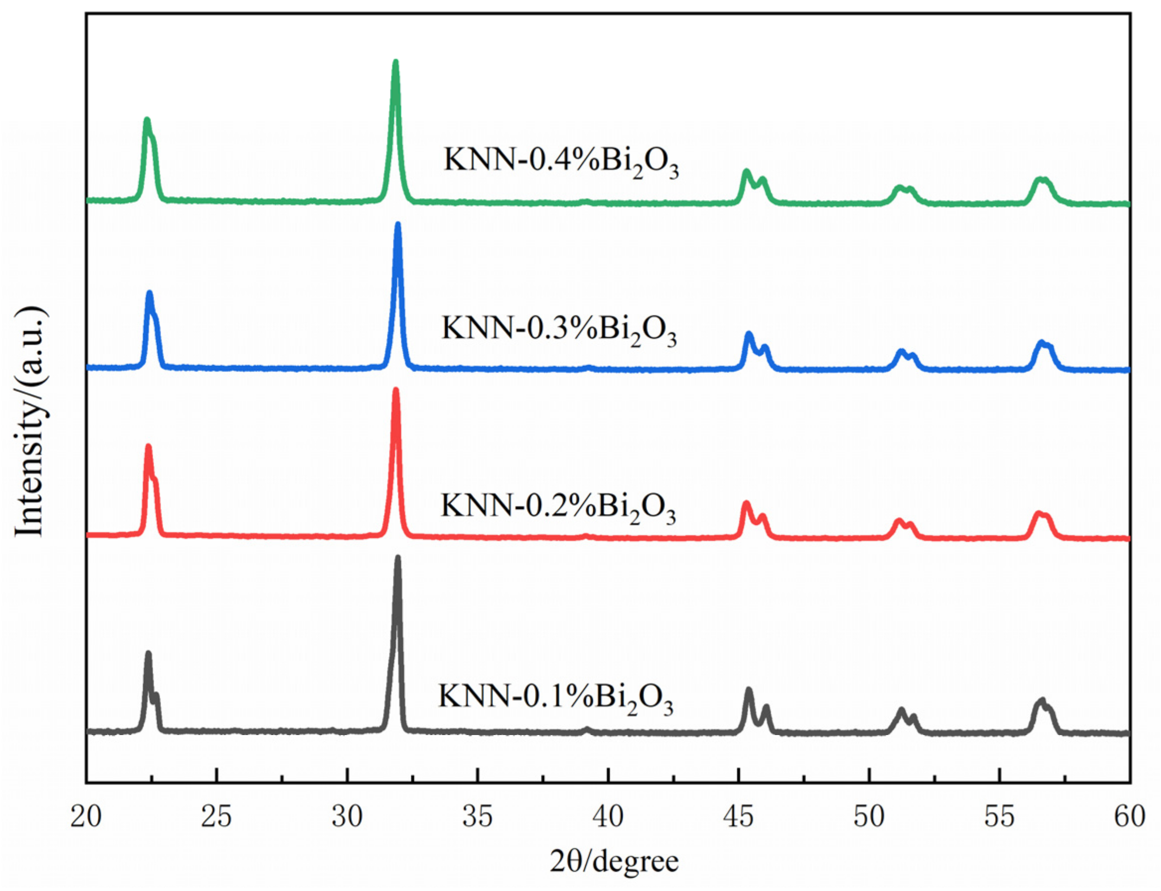
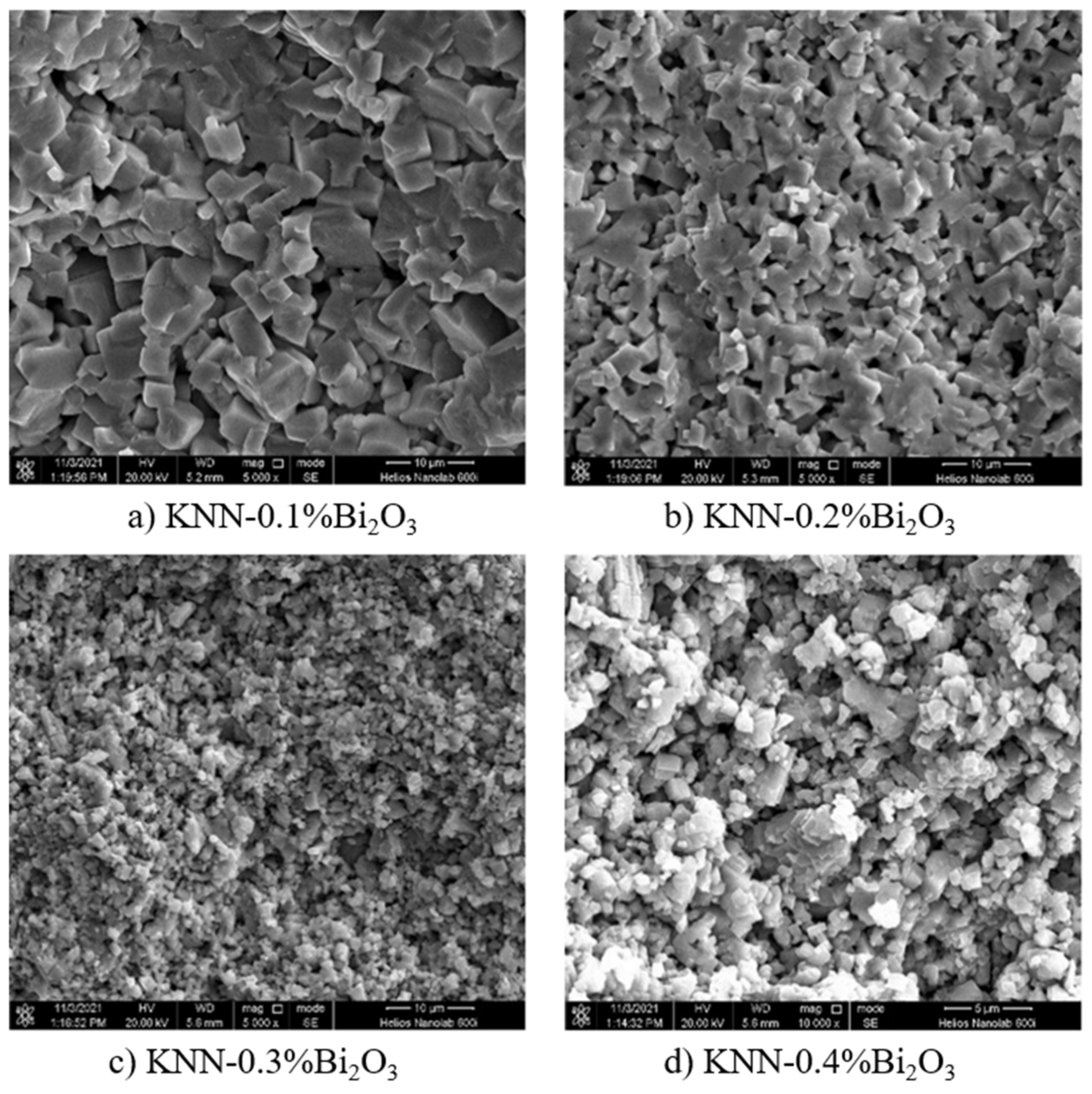
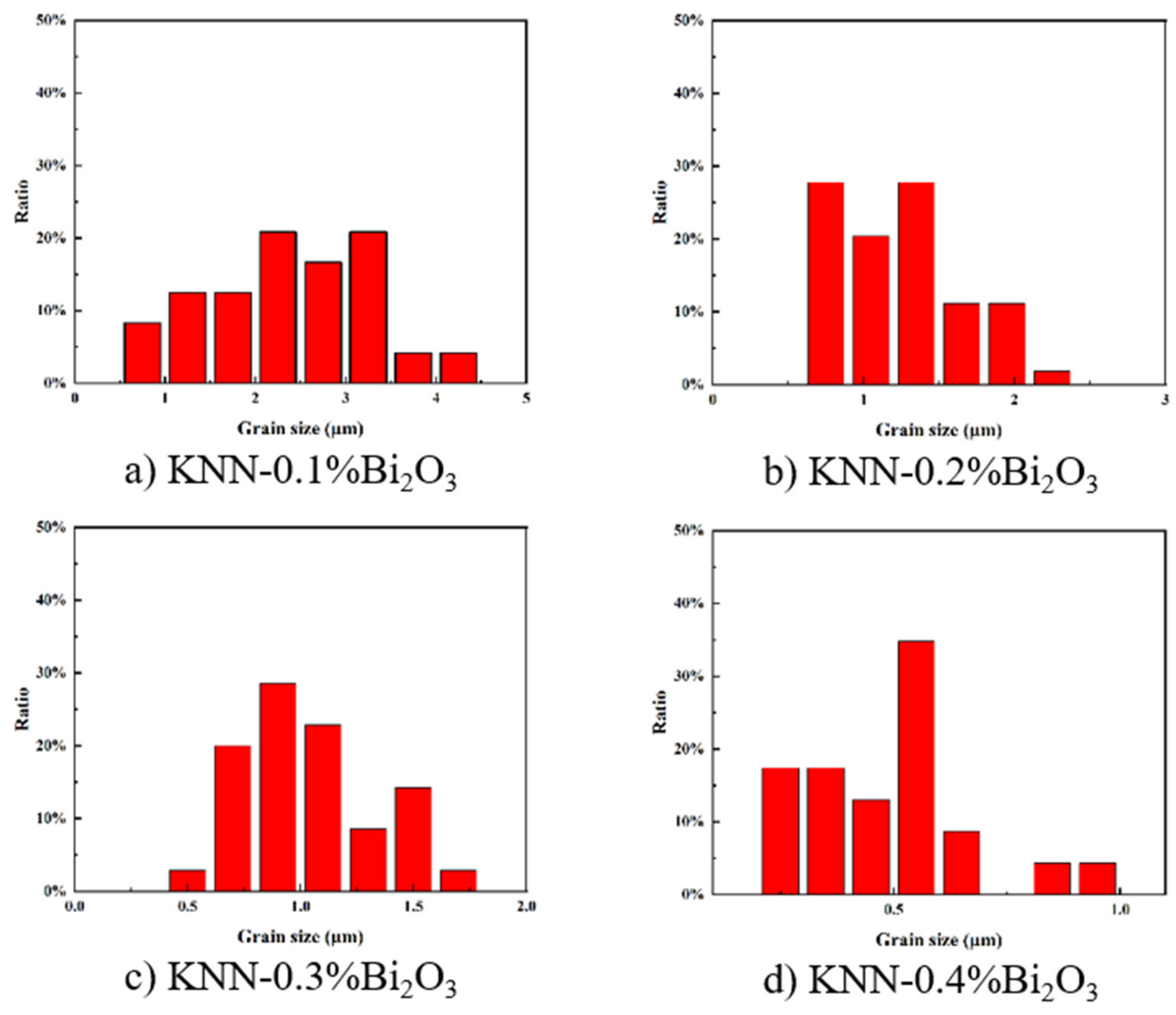
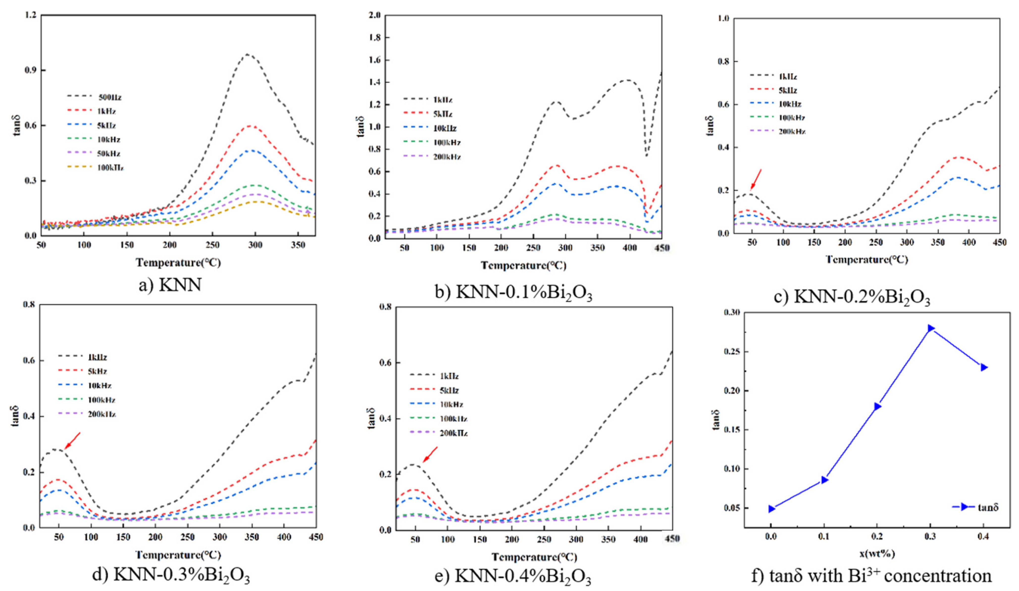
3. Results and Discussions

Figure 1 shows the XRD patterns of KNN-xBi2O3 ceramics, and the test range is from 20° to 60° at room temperature. It can be seen from the XRD pattern that the sample is a perovskite structure with no impurity phase. Table 1 contains the unit cell parameters for KNN-x%Bi2O3(x = 0.0, 0.1, 0.2, 0.3) ceramics. When the doping concentration x is 0.1, the ratio of the peak intensities of the diffraction peaks (220) and (002) is approximately 2:1 at 45°, indicating that the sample is in the orthorhombic phase at room temperature. With the increase in doping concentration, the difference in the peaks (220) and (002) is narrowed, and the ratio of the peak intensities approaches 1.5:1, indicating that the proportion of the trigonal phase in the sample increased and that the orthogonal–trigonal phase was formed at room temperature. The reason for this is that the atomic radius of Bi3+ is larger than that of Na+ and K+, and the oxygen octahedral structure is distorted after the substitution of the A site, which increases the proportion of the trigonal phase in the ceramic at room temperature, and creates an orthogonal–trigonal phase boundary at room temperature.
Figure 2 shows the microscopic topography of KNN-xBi2O3 piezoelectric ceramics, and tetragonal grains can be clearly observed in all samples. Moreover, with the increase in Bi3+ content, the grain size of ceramics gradually decreases. The reason for this phenomenon may be that the atomic radius of Bi3+ is smaller than that of Na+ and K+; the doped Bi is located at grain boundaries and excessive voids inhibit grain growth [29,30]. Therefore, the reduction in grain size occurs because the added Bi3+ replaces the position of the A ion in the ABO3 perovskite structure. From Figure 2a–c, it can be seen that the pores increase with an increase in doped Bi3+ concentration in the ceramics. The melting point of Bi2O3 is lower than the sintering temperature of KNN ceramics, and the liquid phase appears during the sintering process, resulting in an increase in the contact area of the grain boundaries. With an increase in grain boundary mobility, the pore discharge rate becomes lower than the grain growth rate and defects appear in the ceramics.
Figure 3 shows the particle size distribution of the KNN-xBi2O3 piezoelectric ceramics. When the doping concentration x is 0.1, the distribution of grain size is not uniform; the grain size ranges from 0.5 μm to 4.5 μm. With an increase in doping concentration, the grain size decreases and the uniformity of grain size increases. When the doping concentration x is 0.4, the grain size fluctuates around 1 μm and the average grain size reaches the minimum value of 0.49 μm. The SEM data show that Bi2O3 doping can effectively reduce the grain size of the ceramics and improve the uniformity of grains. However, when the doping concentration x is greater than or equal to 0.2, the pores will increase, so the doping concentration of Bi2O3 should be adjusted reasonably.
Figure 4 shows the dielectric temperature spectrum of KNN-xBi2O3 ceramics. The mesothermal spectrum of KNN ceramics is shown in Figure 4a. KNN ceramics have an orthorhombic phase structure at room temperature and undergo trigonal–tetragonal and tetragonal–cubic phase transitions at 209 °C and 304 °C, respectively. Figure 4b–e present the dielectric spectra of KNN-x%Bi2O3 ceramics, corresponding to samples with doping concentrations of 0.1%, 0.2%, 0.3%, and 0.4%. From Figure 4b, it can be observed that there are three distinct peaks in the dielectric temperature map. The peak at 281 °C corresponds to the depolarized dielectric peak. After this peak, the remaining two peaks correspond to the quadrature at 194 °C. The tetragonal phase transition at the dielectric peak and the tetragonal–cubic phase transition dielectric peak at 429 °C. There are also three peaks in Figure 4c–e, which correspond to the orthogonal–trigonal phase transition dielectric peak, the orthorhombic–tetragonal phase transition dielectric peak, and the tetragonal–cubic phase transition dielectric peak, respectively; the corresponding temperatures are 57 °C, 215 °C, and 433 °C, respectively. It can be seen Bi3+ doping can increase the orthogonal–trigonal phase transition temperature of KNN-based ceramics around 50 °C. Figure 4f presents the orthorhombic–tetragonal phase transition temperature and dielectric constant under different concentrations of bismuth oxide doping. Except for individual singular points, the overall trend of the two is an improvement with the increase of bismuth oxide doping concentration. Among them, the overall improvement in TO-T is relatively low, but the dielectric constant is significantly improved. When the doping concentration x was 0.4, the dielectric constant is increased by nearly 30% compared with KNN ceramics. This is because Bi3+ doping increases the proportion of the trigonal phase at room temperature, making the orthogonal–trigonal mixed phase structure at room temperature. Therefore, the dielectric properties of KNN ceramics can be improved by doping Bi3+.
Figure 5 shows the change in dielectric loss during the heating process of KNN-xBi2O3 piezoelectric ceramics. It can be seen that the dielectric loss of the sample changes drastically at the phase transition, which is due to the lattice distortion caused by the phase transition as the temperature increases, resulting in a dramatic increase in dielectric loss. Figure 5f shows the variation in the dielectric loss of the ceramics with Bi3+ content at 50 ˚C and 1 kHz. It can be observed from the figure that the dielectric loss of the sample increases with the increase in doping concentration; moreover, at the Bi3+ content of 0.3, the dielectric loss of the sample reaches its peak value, because the pores increase, causing more defects in the sample, and the dielectric loss increases.
Figure 6a displays the hysteresis loops of KNN-x%Bi2O3 ceramics under the electric field of 25 kV/cm. With the addition of Bi3+, the squareness of the hysteresis loops of the samples increased with the increase in Bi3+ concentration, indicating that the ferroelectric properties of the ceramics also improved with the increase in Bi3+ concentration. The hysteresis loop of the sample with doping concentration x = 0.3 is poor. Combined with SEM data analysis, it was observed that there were many pores in the sample, which result in excessive internal leakage current. Figure 6b shows the relationship between remanent polarization, coercive field, and saturation polarization with doping concentration. Bi3+ doping can soften KNN ceramics, making it easier for domains to flip. The influence of polarization intensity is greater, and they all follow an increasing trend. When the doping concentration x is 0.1, the increase reaches 70%. However, with an increase in the Bi3+ doping concentration, the magnitude will decrease. In addition, the coordination number around the pores may also be increased due to grain size reduction. When the coordination number is greater than or equal to 6, the grain growth will slow down the shrinkage of the pores [29]. The remanent polarization and the maximum polarization of the ceramic decrease.
Table 2 presents the characterization of the piezoelectric properties of KNN-xBi2O3 ceramics, including electromechanical coupling coefficients kp, kt, and piezoelectric constants. A small amount of Bi3+ doping can significantly improve the piezoelectric properties of ceramics. When the doping concentration x is 0.1, d33 reached 121 pC/N. The reason for this is that a small amount of doped Bi3+ entered the lattice, significantly improving the electromechanical coupling coefficient. The thickness of the electromechanical coupling coefficient kt reached 0.306a and the plane electromechanical coupling coefficient kp reached 0.474. When the doping concentration increases, excess Bi3+ will not enter the interior of the lattice, but hinder the growth of grains at the grain boundaries. Although the grain size tends to shrink, there are more pore defects and poorer ceramic performance. The planar electromechanical coupling coefficient of the sample ceramic with a doping concentration of x = 0.3 is the highest among the experimental samples, but its thickness electromechanical coupling coefficient drops to 0.138, the electromechanical coupling coefficients kp and kt cannot be improved, and the piezoelectric performance of the ceramic decreases at the same time.

4. Conclusions

In this paper, KNN-x%Bi2O3 ceramics are prepared by a solid-state reaction method. The doping of Bi element can increase the proportion of the tripartite phase in the ceramic. When the doping concentration x is higher than 0.2%, the orthogonal–tripartite phase boundary is created, which can improve the electrical properties of ceramics. When the doping concentration x is 0.1, the piezoelectric constant reached 121 pC/N. When the doping concentration x is 0.4, the dielectric constant reached a maximum value of 468.03. Therefore, high-performance lead-free potassium niobate nano-ceramics can be prepared by adjusting the phase boundary and grain size by doping with a small amount of Bi2O3.

Author Contributions

Data curation, J.L.; formal analysis, J.L. and H.M.; investigation, J.L. and J.W.; project administration, F.W.; validation, D.L.; writing—original draft J.L. and J.W.; writing—review and editing, T.M., Y.T. and B.Y. All authors have read and agreed to the published version of the manuscript.

Funding

This research was supported by the National Natural Science Foundation of China (NSFC) (No. 51402075) and the Natural Science Foundation of Heilongjiang Province (No. E2018049).

Institutional Review Board Statement

Not applicable.

Informed Consent Statement

Not applicable.

Data Availability Statement

The data presented in this study are available on request from the corresponding author.

Conflicts of Interest

The authors declare no conflict of interest.

References

  1. Egerton, L.; Dillon, D.M. Piezoelectric and dielectric properties of ceramics in the system potassium-sodium niobate. J. Am. Ceram. Soc. 2010, 42, 438–442. [Google Scholar] [CrossRef]
  2. Saito, Y.; Takao, H.; Tani, T.; Nonoyama, T.; Takatori, K.; Homma, T.; Nagaya, T.; Nakamura, M. Lead-free piezoceramics. Nature 2004, 432, 84–87. [Google Scholar] [CrossRef] [PubMed]
  3. Zhou, C.; Zhang, J.; Yao, W.; Liu, D.; He, G. Remarkably strong piezoelectricity, rhombohedral-orthorhombic-tetragonal phase coexistence and domain structure of (K,Na)(Nb,Sb)O3-(Bi,Na)ZrO3-BaZrO3 ceramics. J. Alloy. Compd. 2019, 820, 153411. [Google Scholar] [CrossRef]
  4. Wang, J.; Luo, L. Probing the diffusion behavior of polymorphic phase transition in K0.5Na0.5NbO3 ferroelectric ceramics by Eu3+ photoluminescence. J. Appl. Phys. 2018, 123, 144102.1–144102.7. [Google Scholar] [CrossRef]
  5. Xu, K.; Li, J.; Lv, X.; Wu, J.; Zhang, X.; Xiao, D.; Zhu, J. Superior piezoelectric properties in potassium-sodium niobate lead-free ceramics. Adv. Mater. 2016, 28, 8519–8523. [Google Scholar] [CrossRef] [PubMed]
  6. Qin, Y.; Zhang, J.L.; Yao, W.; Lu, C.; Zhang, S. Domain configuration and thermal stability of (K0.48Na0.52)(Nb0.96Sb0.04)O3-Bi0.50(Na0.82K0.18)0.50ZrO3 piezoceramics with high d33 coefficient. ACS Appl. Mater. Interfaces 2016, 8, 7257–7265. [Google Scholar] [CrossRef] [PubMed]
  7. Li, J.F.; Wang, K.; Zhu, F.Y.; Cheng, L.Q.; Yao, F.Z. (K,Na)NbO3-based lead-free piezoceramics: Fundamental aspects, processing technologies and remaining challenge. J. Am. Ceram. Soc. 2013, 96, 3677–3696. [Google Scholar] [CrossRef]
  8. Dai, Y.J.; Zhang, X.W.; Chen, K.P. Morphotropic phase boundary and electrical properties of K1-xNaxNbO3 lead-free ceramics. Appl. Phys. Lett. 2009, 94, 042905. [Google Scholar] [CrossRef]
  9. Wu, J.; Xiao, D.; Zhu, J. Potassium-Sodium Niobate Lead-Free Piezoelectric Materials: Past, Present, and Future of Phase Boundaries. Chem. Rev. 2015, 115, 2559–2595. [Google Scholar] [CrossRef]
  10. Guo, Y.; Kakimoto, K.I.; Ohsato, H. Phase transitional behavior and piezoelectric properties of (Na(0.5)K(0.5))NbO3-LiNbO3 ceramics. Appl. Phys. Lett. 2004, 85, 4121–4123. [Google Scholar] [CrossRef]
  11. Dai, Y.; Zhang, X.; Zhou, G. Phase transitional behavior in K0.5Na0.5NbO3-LiTaO3 ceramics. Appl. Phys. Lett. 2007, 90, 262903. [Google Scholar] [CrossRef]
  12. Wang, K.; Yao, F.Z.; Jo, W.; Gobeljic, D.; Shvartsman, V.V.; Lupascu, D.C.; Li, J.F.; Redl, J. Temperature-Insensitive (K,Na)NbO3-based lead-free Piezoactuator Ceramics. Adv. Funct. Mater. 2013, 23, 4079–4086. [Google Scholar] [CrossRef]
  13. Du, H.L.; Zhou, W.C.; Luo, F.; Zhu, D.M.; Pei, Z.B. Structure and electrical properties’ investigation of (K0.5Na0.5)NbO3-(Bi0.5Na0.5)TiO3 lead-free piezoelectric ceramics. J. Phys. D Appl. Phys. 2008, 41, 085416. [Google Scholar] [CrossRef]
  14. Hong, T.; Wu, J.; Zheng, T.; Wang, X.; Lou, X. New (1-x)K0.45Na0.55Nb0.96Sb0.04O3-xBi0.5Na0.5HfO3 lead-free ceramics: Phase boundary and their electrical properties. J. Appl. Phys. 2015, 118, 044102. [Google Scholar]
  15. Cheng, X.; Wu, J.; Lou, X.; Wang, X.; Wang, X.; Xiao, D.; Zhu, J. Achieving both giant d33 and high Tc in patassium-sodium niobate ternary system. ACS. Appl. Mater. Inter. 2014, 6, 750–756. [Google Scholar] [CrossRef]
  16. Cheng, X.; Wu, J.; Wang, X.; Zhang, B.; Lou, X.; Wang, X.; Xiao, D.; Zhu, J. Mediating the contradiction of d33 and TC in potassium-sodium niobate lead-free piezoceramics. ACS Appl. Mater. Interfaces 2013, 5, 10409–10417. [Google Scholar] [CrossRef] [PubMed]
  17. Sun, S.; Liu, H.; Fan, L.; Ren, Y.; Chen, J. Structural origin of size effect on piezoelectric performance of Pb(Zr,Ti)O3. Ceram. Int. 2020, 47, 5256–5264. [Google Scholar] [CrossRef]
  18. Huang, X.; Li, W.; Zeng, J.; Zheng, L.; Men, Z.; Li, G. The grain size effect in dielectric diffusion and electrical conduction of PZnTe-PZT ceramics. Physica B 2019, 560, 16–22. [Google Scholar] [CrossRef]
  19. Yu, H.; Wang, X.; Jian, F.; Li, L. Grain size effect on piezoelectric and ferroelectric properties of BaTiO3 ceramics. J. Eur. Ceram. Soc. 2014, 34, 1445–1448. [Google Scholar]
  20. Kakimoto, K.I.; Kaneko, R.; Kagomiya, I. Grain size controlled (Li,Na,K)NbO3 ceramics using powder source classified by centrifugal separator. Jpn. J. Appl. Phys. 2013, 51, 09LD06. [Google Scholar] [CrossRef]
  21. Wang, X.; Yu, H.; Zhao, P.; Liu, X.; Wei, T.; Zhang, Q.; Wang, X. Optimizing the grain size and grain boundary morphology of (K,Na)NbO3-based ceramics: Paving the way for ultrahigh energy storage capacitors. J. Mater. 2021, 7, 780–789. [Google Scholar] [CrossRef]
  22. Wang, C.; Chen, J.; Shen, L.; Rui, J.; Hou, Y. Particle size effect on the electrical properties of spark-plasma-sintered relaxor potassium sodium niobate ceramic. J. Ceram. Sci. Technol. 2017, 8, 255–258. [Google Scholar]
  23. Cha, J.M.; Lee, J.W.; Bae, B.; Yong, J.J.; Yoon, C.B. Synthesis and characterization of MnO2 added (Na0.475K0.475Li0.05) (Nb0.9Ta0.05Sb0.05)O3 lead-free piezoelectric ceramics. J. Korean Ceram. Soc. 2020, 57, 440–446. [Google Scholar] [CrossRef]
  24. Ar, A.; Spa, C.; Ym, A.; Gth, A.; Jjc, A.; Bdh, A.; Khc, B.; Sn, D.; Cwa, A. An easy approach to obtain large piezoelectric constant in high-quality transparent ceramics by normal sintering process in modified potassium sodium niobate ceramics. J. Eur. Ceram. Soc. 2020, 40, 2989–2995. [Google Scholar]
  25. Wang, X.; Tang, X.; Kwok, K.; Chan, H.; Choy, C.L. Effect of excess Bi2O3 on the electrical properties and microstructure of (Bi1/2Na1/2)TiO3 ceramics. Appl. Phys. A 2005, 80, 1071–1075. [Google Scholar] [CrossRef]
  26. Li, S.; Fu, J.; Zuo, R. Middle-low temperature sintering and piezoelectric properties of CuO and Bi2O3 doped PMS-PZT based ceramics for ultrasonic motors. Ceram Int. 2021, 47, 20117–20125. [Google Scholar] [CrossRef]
  27. Yang, W.; Li, P.; Wu, S.; Li, F.; Shen, B.; Zhai, W. A study on the relationship between grain size and electrical properties in (K,Na)NbO3-Based lead-free piezoelectric ceramics. Adv. Electron. Mater. 2019, 5, 1900570. [Google Scholar] [CrossRef]
  28. Liu, Y.; Li, Z.; Thong, H.; Lu, J.; Li, J.; Gong, W.; Wang, K. Grain size effect on piezoelectric performance in perovskite-based piezoceramics. Acta Phys. Sin. 2020, 69, 217704. [Google Scholar] [CrossRef]
  29. Bah, M.; Podor, R.; Retoux, R.; Delorme, F.; Nadaud, K.; Giovannelli, F.; Monot-Laffez, I.; Ayral, A. Real-Time Capturing of Microscale Events Controlling the Sintering of Lead-Free Piezoelectric Potassium-Sodium Niobate. Small 2022, 2106825. [Google Scholar] [CrossRef]
  30. Cahn, J.W. The impurity-drag effect in grain boundary motion. Acta Metall. 1962, 10, 789–798. [Google Scholar] [CrossRef]
Figure 1. XRD pattern of KNN-xBi2O3 piezoelectric ceramics.
Coatings 12 00526 g001
Figure 2. SEM of KNN-xBi2O3 piezoelectric ceramics.
Coatings 12 00526 g002
Figure 3. Particle size distribution of KNN-xBi2O3 piezoelectric ceramics.
Coatings 12 00526 g003
Figure 4. Temperature dependence of dielectric permittivity and TO-T, and dielectric constant ε r dependence for KNN-x%Bi2O3(x = 0.0, 0.1, 0.2, 0.3, 0.4) ceramics.
Coatings 12 00526 g004
Figure 5. Temperature dependence of dielectric loss tanδ for KNN-x%Bi2O3(x = 0.0, 0.1, 0.2, 0.3, 0.4) ceramics.
Coatings 12 00526 g005
Figure 6. Ferroelectric properties of KNN-xBi2O3 piezoelectric ceramics.
Coatings 12 00526 g006
Table 1. Cell parameters of KNN-x%Bi2O3(x = 0.0, 0.1, 0.2, 0.3) ceramics.
x (wt%)0.10.20.3
a(Å)3.96553.98013.9700
b(Å)5.74825.68415.6846
c(Å)5.63445.71305.7064
Table 2. Electromechanical coupling coefficient of KNN-xBi2O3 ceramics.
x (wt%)0.10.20.30.4
kp0.4740.2760.4780.270
kt0.3060.1660.1400.145
d33(pC/N)121818082
Publisher’s Note: MDPI stays neutral with regard to jurisdictional claims in published maps and institutional affiliations.

