Article

Investigations on the Influence of Subsequent Electron Beam (EB) Remelting on the Microstructure of an Aluminium Nitride Layer Formed on an Aluminium Substrate (Part II)

1
Institute of Materials Engineering, Technische Universität Bergakademie Freiberg, 09599 Freiberg, Germany
2
Institute of Materials Science, Technische Universität Bergakademie Freiberg, 09599 Freiberg, Germany
*
Author to whom correspondence should be addressed.
Coatings 2022, 12(5), 650; https://doi.org/10.3390/coatings12050650
Submission received: 13 April 2022 / Revised: 2 May 2022 / Accepted: 5 May 2022 / Published: 10 May 2022

Abstract

:
Nitriding of Al alloys leads to the formation of a thin, hard nitride layer (AlN) on the surface. A subsequent EBR can both eliminate the nitriding-related cavities under the nitride layer and increase the hardness of the substrate without melting or destroying the nitride layer. This paper deals with investigations regarding the influence of the energy/heat input on the microstructure within both the AlN layer and the remelted Al substrate. Of particular interest was the interface between the AlN and the Al substrate, which changed to a transition zone with a depth of approximately 80 µm. A range of high-resolution imaging and analytical tools for both scanning and transmission electron microscopy were used for these investigations. Based on the findings from the microstructural investigations, a schematic model was developed of the processes occurring within the nitride layer and at the interface as a result of remelting.

1. Introduction

For Fe-based materials, nitriding is a well-known thermochemical surface technology to improve both tribological and corrosive stress behaviour, as well as fatigue strength. This is due to the formation of a thin but very hard compound layer of iron nitrides. In the case of alloyed steels whose alloying elements form special nitrides, this layer is supported by a thicker, hardened diffusion layer.
A hardness or stress profile within the surface similar to that of steel would also be desirable for relatively soft Al-based materials. However, the Al-specific nitriding mechanism—i.e., that of exclusively outward nitride layer growth—leads to strong limitations with respect to the load-bearing capacity of the thin, hard AlN layer formed [1,2]. This is mainly determined by two factors: (i) the lack of a supporting diffusion layer (nitrogen does not exhibit significant solubility in aluminium), and (ii) the formation of local cavities below the AlN layer [1,3,4].
It has already been shown that hardness can be increased by subsequent heat treatment consisting of solution annealing and ageing [5,6,7], as well as by the duplex treatment of EB surface alloying and nitriding [8]. However, for both technology variants, the cavities cannot be eliminated.
Therefore, a new technology aims at the subsequent electron beam remelting (EBR) of a previously nitrided Al material. As has already been shown, this treatment variant offers completely new possibilities for improving the material’s surface properties [9,10,11]. The basis for this special process sequence is both the significantly higher decomposition (1700 °C) and melting temperatures of the AlN (2490 °C) [12] than that of the Al base material (<660 °C). This allows melting of the Al substrate surface underneath the already generated AlN layer (1st process) without melting and thus destroying it. Nevertheless, the energy input must be well dosed in order to avoid negatively influencing the AlN layer in terms of both its microstructure and properties. Therefore, the microstructural components of AlN layers as well as their physical properties are of great importance for subsequent surface remelting.
To date, this treatment sequence has only been implemented in association with a subsequent solid-phase process, such as surface hardening for thin nitrided layers or hard coatings deposited on steels [13].
Electron beam liquid-phase processes are characterized by high cooling rates (102–105 K/s [14]) after surface remelting, which usually lead to solidification under disequilibrium conditions. In some cases, metastable or completely new phases are precipitated [15]. Furthermore, the solid solution solubility increases [16,17]. In the case of Fe and Zr in Al, the solubility increases from <1 at.% to as much as 10 at.%. For Mg, Si and Cu, as much as 40 at.% can be achieved. However, the information on maximum solubility varies greatly in the literature [18]. Investigations have shown that the rapidly cooled microstructure after spray compacting changes fundamentally after remelting. A dendritic cast structure is formed with eutectic Si precipitates and a supersaturated solid solution. With increasing cooling rate, the Si content in the eutectic can be increased from an original value of about 12 wt.% to as high as 19 wt.% [19]. In addition, new or morphologically altered intermetallic phases are formed [18,20]. This effect strongly depends on the initial chemical composition. Alloying elements such as Cu, Ni and Fe and the intermetallic phases they form have a major influence on the hardness of the remelted layer [8]. In contrast, Si precipitations play something of a subordinate role in changing the hardness of the layer. As a result of microstructural refinement and phase formation, there is typically a 2- to 3-fold increase in hardness after remelting of spray-compacted Al alloys, depending on the cooling rate and chemical composition [11,18].
On the basis of a detailed understanding of the microstructural features of the initial nitrided state presented in part I (see [21]), the changes during subsequent electron beam remelting are investigated in the present work. This applies to both the effects on the AlN layer, with its different phases, as well as the Al base material as a result of short-term remelting, and especially at the interface.
A deep understanding of the mechanisms and microstructural changes evident after the single and combination processes will form the basis for the future generation of a load-optimized surface composite according to the duplex treatment of PN + EBR.

2. Materials and Methods

2.1. Material

The spray-formed hypereutectic Al alloy DISPAL S232® (Supplier: Gränges Powder Metallurgy GmbH, Velbert, Germany formerly PEAK Werkstoff GmbH, ibid) was used as the base material. A detailed description of its microstructure can be found in Part I of this research work [21].

2.2. Surface Treatment Technologies and Parameters

Plasma nitriding (1st process step) was carried out in a commercial DC plasma nitriding facility under soft vacuum conditions (15 Pa). The aim of parameter setting (see [21]) was the generation of different nitride layer thicknesses tAlN in the range of 1.5 to 4.3 µm.
In a 2nd process step, EB remelting (EBR) of a small surface area of the Al substrate underneath the already existing AlN layer was carried out in a universal electron beam facility K26-15/80 (power: 15 kW; max. acceleration voltage: 80 kV) from pro-beam systems GmbH (Stollberg, Germany). Due to the process, the treatment takes place in a vacuum chamber with a soft vacuum of approximately 0.1–1 Pa. Therefore, two different beam guidance techniques—line scan and meander—were used (see schematic illustration in [10,11]). In the case of the line scan, the EB is deflected along a line at high frequency in the y-direction (5000 Hz) and the specimen is fed perpendicularly in the x-direction (vx = 8–12 mm/s). This results in a path-shaped energy transfer, the width of which is determined by the line length (ly = 10 mm). The energy distribution is almost constant over the line length.
With the meander technique, the EB is guided in a meandering manner over the sample surface by a combined movement of beam deflection in the y-direction and sample displacement in the x-direction. With a relatively slow beam deflection in the y-direction (fy = 5–10 Hz), a discrete melt pool can be seen on the surface compared to the line scan, which is deflected over a path width of b = 10 mm. In the process, the melt tracks created transverse to the sample feed (vx = 1.6–2 mm/s) merge with each other in such a way that a closed remelting path is created. The beam was additionally superimposed by a circular oscillation figure (dosz = 0.5–0.75 mm, fosz = 500–800 Hz).
The EBR layer thickness tEBR was varied by means of variations of the beam current IB mainly.
Thermographic measurements (thermo field camera P1-ML (Optris GmbH, Berlin, Germany) on the surface of the AlN layer during EB remelting revealed maximum hotspot temperatures of approximately 1200 °C. These are far below the decomposition or melting temperature of the AlN (cf. Section 1), but they are twice as high as the melting temperature of the Al substrate. As a result, only the Al surface melted up to an energy-dependent depth z.

2.3. Characterization Methods

The process-specific surface deformations after EBR were characterized by non-contact 3D surface profilometry.
The microstructures were analysed by means of metallographic cross sections using light optical microscopy (LOM) and scanning electron microscopy (SEM). In addition to microstructural investigations, the AlN layer thickness tAlN, the EBR layer thickness tEBR and the height difference Δh resulting from surface deformation during remelting were measured on the transverse sections. The above mentioned geometric parameters were determined for each parameter variant on three light microscope images at 2 to 5 measuring points each and then averaged.
SEM images were used to determine the secondary dendrite arm spacing (SDAS). However, the SDAS values were only an estimate, as they were not determined according to recognized standards. With the help of the SDAS, the local solidification time t could be estimated according to Equation (1), using the material specific constant k = 10.4 µm/s−⅓ (for AlSi10Mg [22]). Meanwhile—and considering the solidification interval (Ts–l) for DISPAL S232 (216 K [23,24])—the cooling rate T ˙ was estimated according to Equation (2).
S D A S = k · t 3
T ˙ = T s l t
Transmission electron microscopy JEM 2200FS (JEOL GmbH, Munich, Germany) was used for spatially resolved (AlN layer, interface/transition zone, remelted base material) detailed microstructural characterisation. A comprehensive description of the sample preparation procedures and the high-resolution analytical tools are given already by the authors in Part I [21].
The nanoindentation was performed inside a scanning electron microscope (SEM) using a Picoindenter (PI 87, Hysitron, Minneapolis, MN, USA) mounted on the SEM stage. Hardness-depth curves were recorded in the nitride layer starting from the surface and extending up to the remelted surface of the Al substrate. The indentations were performed using a Berkovich indenter in displacement-controlled mode with a maximum depth of zmax = 60 nm (nitrided state, PN) and zmax = 80 nm (nitrided and remelted state, PN + EBR). The specimen was tiled by 70° relative to the electron beam during the measurement process.
The layers generated in the course of the development of this remelting technology were characterised on the basis of hardness-depth curves by means of microhardness measurement HV0.3 (FN = 2.98 N).

3. Results and Discussion

3.1. Initial Plasma Nitrided State (PN)

For the preliminary investigations on the influence of the EB parameters on the formation of the EB remelted layer, AlN layers with thicknesses in the range of 1.5 to 5.4 µm were used (see Section 3.2).
The different layer thicknesses were mainly achieved by varying the effective nitriding time, i.e., the longer the time, the thicker the layer. Detailed information on the nitriding technology and the results observed can be found in the literature [21,25,26].
The main challenges in layer formation as a result of the plasma nitriding of spray-compacted Al alloys are that of local cavity formation due to outward Al diffusion (Figure 1a) and the selective growth of nitride nuclei in the area of the Al solid solution, which led to gap formation at the interface (Figure 1b).
The nitrided initial state, which was suitable for detailed investigations by means of high-resolution imaging and analytics after the duplex treatment (PN + EBR) within the context of this contribution, is characterised comprehensively in Part I of this research work [21].

3.2. Influence of the AlN Layer Thickness on the Subsequent Electron Beam Remelting Process (PN + EBR)

Given a constant AlN layer thickness, previous works by the current authors describe the influence of different beam deflection techniques—such as the flash technique [10], the meander technique and the line scan technique [11]—on the microstructure and hardness of the remelted layers.
This contribution investigates the influence of both different AlN layer thicknesses and energy inputs (beam current IB at a constant feed rate vx) for two different deflection techniques (line scan, meander).
As expected, the remelting depth increased almost linearly with increasing energy input or increasing beam current IB (red curve in Figure 2a) with the line scan method. In principle, this relationship also applies to the combination treatment (PN + EBR) if the energy input takes place via the AlN layer formed on the surface. Depending on the initial AlN layer thickness; however, there were deviations with regard to the EBR layer thickness achieved compared to the single treatment (EBR), i.e., without AlN. Assuming the same energy input, AlN initial layer thicknesses of tAlN ≤ 3 µm led to lower—and tAlN ≥ 4.5 µm to higher—EBR layer thicknesses than those achieved by EBR of the unnitrided Al material (cf. Figure 2a). For an AlN initial layer thickness of approximately 4 µm, the EBR layer thicknesses achieved for single and duplex treatment were of a similar magnitude (Figure 2a).
With the meander technique, such a clear dependency on both the energy input and the initial AlN layer thickness could not be detected (Figure 2b). The energy input represented by the beam current IB could only be varied in a narrow range. A beam current of IB = 1.6 mA or a layer thickness of approximately 50 µm represented a limit state where the AlN layer thickness had a strong influence on the results achieved. While no defects could be found within the EBR layer for thinner AlN layers (cf. area I. for IB = 1.6 mA, Figure 2b), remelting in association with thicker AlN layers tended to lead to defects, such as layer spalling (cf. area II. for IB = 1.6 mA, Figure 2b).
During EBR close to the surface, on the one hand, a volume expansion occurred during the generation of the melt pool, which was a function of the thermal expansion coefficient of the Al alloy DISPAL S232 (α = 18–19 · 10−6 K−1) and the temperature difference (ΔT = 1100 K). This could be roughly estimated on the basis of the linear expansion perpendicular to the sample surface and amounted to approximately Δz = 1 µm for a relevant remelting depth of 50 µm.
On the other hand—and of far greater significance—the local cavities that resulted from the outward diffusion of aluminium during nitriding were filled by the melt (Figure 3b). The temperature- and concentration-dependent melt movement (Marangoni flow) led to swelling of the surface, with some highly geometric patterns at the surface. In the cross section, a relatively uniform wave profile is recognisable, which is characterised by a height difference Δh (cf. Figure 3a). The evaluation of all determined height differences (as described in Section 2.3) showed that the AlN layers are predominantly damage tolerant up to a height difference of Δhmax < 16 µm, i.e., they can deform and do not lead to spalling on the surface (see exemplarily A in Figure 4a, tAlN = 1.6 µm). Depending on the thickness of the AlN layer and/or the EBR parameters, some spalling of the AlN layer occurred locally (B in Figure 4a, tAlN = 4.3 µm).
EDS measurements proved that even after the combination treatment (PN + EBR), the AlN layer was enriched with Mg and Al (Figure 4b). Initially, this suggested that, compared to the initial AlN layer (see [21]), no changes in either the elemental distribution or, perhaps, the microstructure occurred after EBR as a result of the thermal exposure.
Similarly to the findings shown elsewhere by the authors [9,10,11,18,20], the rapid solidification of the melt pool generated in the surface of the Al substrate beneath the AlN layer resulted in a hardness level that was up to three times higher than that of the base material. The reason for this was the formation of a new microstructure under non-equilibrium conditions (see needles in SEM micrograph in Figure 4b). This led to the formation of various intermetallic phases, which will be described later.

3.3. High-Resolution Analysis of the Single and Duplex Treatment

3.3.1. Single Treatment: Electron Beam Remelting (EBR)

As already mentioned, the remelted microstructure was so fine—due to the rapid solidification—that the microstructural components could hardly be resolved under the light microscope. TEM images showed that a cellular dendritic structure and various intermetallic phases (IC) had formed (Figure 5a).
The cells consisted predominantly of Al solid solution. In contrast to the initial spray compacted state (cf. [21]), additionally very fine globular crystallites were seen within the cells (see I. in Figure 5c) and in the intercellular region (II. in Figure 5c) in the bright-field (bf) contrast of the TEM image. In both regions, beside Al additionally Si could be detected by means of EDS measurement (point A, B in Figure 5d). Furthermore, fine-range diffraction confirmed the presence of Si (Figure 5e). The Si crystallites exhibited a size of between 10–20 nm and—in isolated cases—as much as 50 nm (Figure 5c). It was concluded from the diffraction images that the grains were statistically randomly oriented and, thus, produced closed diffraction rings. From the findings, it can be concluded that the silicon that was exclusively precipitated primarily in the initial state is now eutectically precipitated, especially in the intercellular region.
A cell size of 0.15–0.25 µm was determined on the basis of the TEM images (cf. Figure 5a). It should be noted that this was only an estimate and not a standard-compliant determination of SDAS. A cooling rate of approximately 10−3 K/s was calculated according to Equations (1) and (2).
In the analysis range of a few μm, it could be concluded from the diffraction patterns that the Al matrix within the cells (CCR)—as well as in the intercellular region (ICR)—were of similar orientation. As with a casting texture, the dendrites were oriented towards the heat flux in the direction of the base material. From the <116> beam direction in the TEM, directional solidification resulted parallel to the heat flow near the <110> direction or plane (identical in the cubic crystal system) (see Figure 5f).
Long, acicular AlxFeySiz phases contained no or only minor fractions of Cu (cf. analysis point C in Figure 5b,d). Smaller intermetallic phases embedded in the dendritic matrix microstructure exhibited equal proportions of Fe and Cu alongside the primary fractions of Al and Si (cf. analysis points D in Figure 5b,d).

3.3.2. Duplex Treatment: Plasma Nitriding + Electron Beam Remelting (PN + EBR)

The energy input of the electron beam changed the interface between the nitride layer and the substrate as a result of the rapid melting and solidification during EBR. The cavities resulting from nitriding were filled with molten aluminium (Figure 3). As a result, the clear assignment of the interface in the merely nitrided state transformed into a transition area, the boundaries of which could not be determined precisely on the basis of the microstructure (cf. Figure 6a). An approximately 50 to 200 nm-wide mixing or transition zone of solidified Al melt and AlN was formed.
EDS measurements should first provide information about changes in the chemical composition within the transition zone formed. It should be noted that reliable determination of the light elements nitrogen and oxygen is not possible with this method, so that only normalized proportions can be given.
An EDS line scan at the interface EBR layer to the AlN layer (Figure 6a) proved that the Mg enrichment already found in the nitrided initial state also persisted after remelting (Figure 6b). In contrast to the nitrided state [21], a significant Si content was also detectable within the AlN layer (Figure 6b). The Fe and Cu contents were at a comparable, though low level and only occurred locally. By means of EEL spectroscopy, it could be proven—in principle—that both O and N were present in this area. However, no statement could be made about their concentrations.
SAED analysis of different parts (I. lower; II. middle; III. upper; see Figure 7) of the AlN layer after EB treatment revealed that the upper part of the AlN layer (III.) was not affected (Figure 7d,e). Analogous to the merely nitrided initial state previously investigated [21], the EELS spectrum of the upper part showed two strong peaks for AlN and Al (diffusion paths) (Figure 7e). In contrast, a peak for AlN was visible in the middle part of the layer (II., Figure 7c), but it was strongly broadened in the direction of the Si peak (Figure 7e). The spectrum also showed an elevation in the area of the Al peak, though there was no clear maximum, but rather a similar broadening. It was obvious that melting of the Al present in the initial state (i.e., former Al diffusion paths) occurred here as a result of the energy input. The EEL spectrum in the lower area of the AlN layer (I., Figure 7b) was similar to that of the middle area, with a somewhat clearer Si peak (Figure 7e). It was thus concluded that the Si could rise into the middle part of the AlN layer via the transition region. As a result of the rapid solidification, a fine Al-Si eutectic formed, which led to broadening of the peak.
Additional fine-range diffraction was carried out in the transition zone between the AlN and the EBR layers (circle area I. (b) in Figure 7b). In the radial intensity distribution, a very high proportion of MgO was detected in addition to AlN and Si (Figure 8c). The intensity distribution of this oxide showed that the MgO was polycrystalline and was present in a preferred orientation (texture). The inner rings of the diffraction pattern were assigned to Si (Figure 8a).
Furthermore, in the transition zone {211} reflections of Mg3N2 were detected by means of diffraction patterns (Figure 8b). Despite the relatively low decomposition temperature (approximately 800 °C), the thermal effect of the EB could not decompose the nitride. This can be explained by the fact that the introduced energy of the EB decreases continuously starting from the surface, so that in the transition zone between substrate and EBR layer was a maximum temperature that is lower than the melting temperature of the substrate (516–738 °C).
Since Mg3N2 was present next to the molten Al, a reaction to AlN was conceivable.

3.3.3. Characterization of Layer Hardness

Hardness-depth profiles were recorded by means of nanoindentation using a Picoindenter in the SEM. Due to surface rounding during sample preparation, the interface between the AlN and the Al substrate was taken as a reference point, i.e., z = 0 µm (Figure 9a). Therefore, hardness measurements in the AlN layer exhibited negative depth values (−z), with positive depth values (z) in the Al substrate. It should be noted that the nanoindentation was carried out under different displacement-controlled test conditions for the treatment states investigated, namely zmax = 60 nm (PN) and zmax = 80 nm (PN + EBR). For this reason, the absolute values of the hardness measurements were not directly comparable. The hardness values after the combination treatment PN + EBR normally tend to be underestimated.
EBR led to nearly four-times-higher hardness (4.6 ± 0.6 GPa) than the initial hardness of the Al substrate. As a result of the thermal influence on the AlN layer during subsequent remelting, there was obviously a homogenisation of the hardness values in the nitride layer (Figure 9b)—values that were strongly scattered in the initial state (cf. [21]). While the average hardness value of the AlN layer after EBR was 13.1 ± 0.6 GPa, the hardness within the transition zone was lower (10.1 ± 1.5 GPa).

3.4. Model Conception for the Formation of the Interface after EB Remelting

On the basis of the TEM investigations in the previous [21] and present contributions, a detailed understanding of the processes involved in nitriding and subsequent remelting was gained. The essential microstructural changes after remelting in comparison to the initial nitrided state were schematically summarised in a model (Figure 10).
After nitriding an Al alloy, as known, an AlN layer is formed on the surface. For the outward nitriding process, Al diffusion paths (Figure 10a) were detected by means of unbound Al that probably accumulated in the region of the AlN crystallite boundaries [21]. Enrichment with Mg occurred at the interface to the Al substrate, which led to the additional formation of both MgO and Mg3N2 [21].
After EBR with suitable parameters, the AlN layer remained fundamentally unaffected. A decisive difference to the merely nitrided state was that the cavities (Figure 10a) formed there had now been filled with melt and, thus, were eliminated after EBR (Figure 10b). Furthermore, the small (but, in the lower-layer section, in particular, wider) gaps between the AlN rods (see Figure 10a) were also filled with Al melt. As a result, a homogeneous transition zone was generated that exhibited continuous bonding of the AlN layer to the substrate. In the lower (transition zone) as well as in the middle part of the AlN layer, additional Al and Si were detected. It was assumed that this formed within the pre-existing Al diffusion paths during the previous nitriding process (cf. Al in Figure 10a). The fine cellular dendritic solidification of the Al melt resulted from the extremely high heating and cooling rates within these small channels. As a result, all of the spaces between the individual AlN rods were infiltrated with melt (due to capillarity) in a quasi-sponge-like manner (Figure 10b).

4. Conclusions

Combination surface treatments have great potential for improving properties that transcend the known possibilities offered by single surface treatments. This was the motivation for the present research work, which dealt with in-depth microstructural investigation of the duplex treatment plasma nitriding and electron beam remelting of a spray-compacted Al alloy. Within the scope of this contribution, the following conclusions could be reached:
(1)
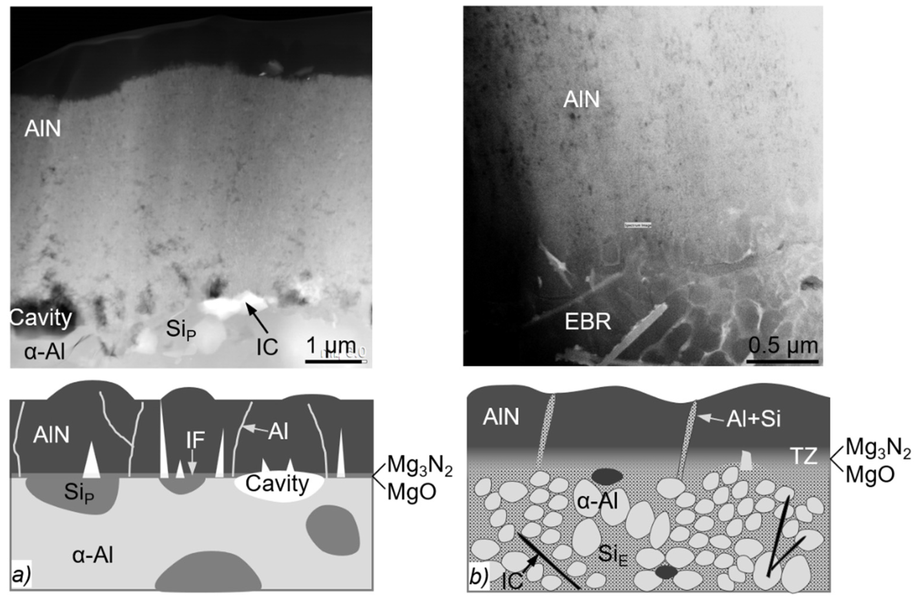
EBR of the Al substrates beneath the AlN layer led to the formation of a fine dendric Al matrix microstructure with different intermetallic compounds.
(2)
In addition to an increase in hardness in the remelted layer, the special innovation of the technology lies in the fact that it was also possible to eliminate (i.e., to “fill”) both the cavities underneath the AlN layer resulting from outward diffusion of the Al and the small gaps between the AlN rods. As a result, a homogeneous transition zone was generated that exhibited continuous bonding of the AlN layer to the substrate.
(3)
Despite the high temperature during the EBR, the transition zone exhibited both AlN and Mg3N2. Furthermore, large amounts of MgO were detected in a polycrystalline structure with a preferential orientation. In the lower (transition zone) as well as in the middle part of the AlN layer, additional Al and Si were detected, the radial intensity distribution peaks of which were strongly broadened and washed out. This was obviously due to the fine cellular dendritic solidification of the Al melt.
(4)
The subsequent remelting led to homogenisation of the hardness values in the nitride layer.
(5)
Due to movement of the melt pool, the surface was structured with a relatively regular pattern and defects, both within and below the AlN layer, were filled with Al melt. It is expected that both should have beneficial effects on the material’s wear behaviour. The research on this matter has not yet been completed.

Author Contributions

Conceptualization, funding acquisition, project administration, supervision, writing—original draft preparation, visualization, A.B.; investigation, writing—review and editing, J.B.; investigation, methodology, investigation, review and editing, E.H. and A.J.; investigation, M.M. and V.K. All authors have read and agreed to the published version of the manuscript.

Funding

This research was funded by German Research Foundation (DFG), grant number AlN-Flash-I and -II (No. BU2568/6-1; 9-1). Open Access Funding by the Publication Fund of the TU Bergakademie Freiberg.

Institutional Review Board Statement

Not applicable.

Informed Consent Statement

Not applicable.

Data Availability Statement

Not applicable.

Acknowledgments

The authors would also like to thank A. Dalke (TU Bergakademie Freiberg, Institute of Materials Engineering) for carrying out the nitriding experiments. The TEM samples were prepared by A. Leuteritz (TU Bergakademie Freiberg, Institute of Materials Science). The authors also wish to thank G. Bittner and R. Lehnert (both TU Bergakademie Freiberg, Institute of Materials Engineering) for carrying out the nano- and pico-indentation hardness measurements.

Conflicts of Interest

The authors declare no conflict of interest.

References

  1. Spies, H.-J.; Dalke, A. Nitriding of Aluminum and its Alloys. In ASM Handbook, Heat Treating of Nonferrous Alloys; Totten, G.E., Ed.; ASM International: Materials Park, OH, USA, 2016; Volume 4E, pp. 302–307. [Google Scholar] [CrossRef]
  2. Telbizova, T.; Parascandola, S.; Kreissig, U.; Günzel, R.; Möller, W. Mechanism of diffusional transport during ion nitriding of aluminium. Appl. Phys. Lett. 2000, 76, 1404–1406. [Google Scholar] [CrossRef]
  3. Spies, H.-J. Stand und Entwicklung des Nitrierens von Aluminium- und Titanlegierungen. HTM J. Heat Treat. Mater. 2000, 55, 141–150. [Google Scholar] [CrossRef]
  4. Buchwalder, A.; Dalke, A.; Spies, H.-J.; Zenker, R. Plasma nitriding of spray-formed aluminium alloys. Adv. Eng. Mater. 2012, 13, 970–975. [Google Scholar] [CrossRef]
  5. Reinhold, B.; Naumann, J.; Spies, H.-J. Einfluss von Zusammensetzung und Bauteilgeometrie auf das Nitrierverhalten von Aluminiumlegierungen. HTM J. Heat Treat. Mater. 1998, 53, 329–336. [Google Scholar] [CrossRef]
  6. Reinhold, B. Untersuchungen zum Einfluss des Sauerstoffpartialdrucks beim Plasmanitrieren von Aluminiumlegierungen und chromlegierten Stählen. Ph.D. Thesis, TU Bergakademie Freiberg, Freiberg, Germany, 2004. [Google Scholar]
  7. Buchwalder, A.; Spies, H.-J.; Zenker, R.; Dalke, A.; Krug, P. Plasmanitrieren von sprühkompaktierten Al-Legierungen. HTM J. Heat Treat. Mater. 2011, 66, 240–247. [Google Scholar] [CrossRef]
  8. Dalke, A. Beitrag zur kombinierten Randschichtbehandlung von Aluminiumlegierungen: Elektronenstrahlumschmelzlegieren mit Fe-Basis-Zusatzstoffen und Plasmanitrieren. Ph.D. Thesis, TU Bergakademie Freiberg, Freiberg, Germany, 2016. [Google Scholar]
  9. Hegelmann, E.; Jung, A.; Buchwalder, A.; Zenker, R. Investigation of electron beam surface remelting of plasma nitrided spray-formed hypereutectic Al-Si alloy. In Proceedings of the 26th DTZ Jihlava, Jihlava, Czech Republic, 21–23 November 2017. [Google Scholar]
  10. Jung, A.; Buchwalder, A.; Hegelmann, E.; Hengst, P.; Zenker, R. Surface engineering of spray-formed aluminium-silicon alloys by plasma nitriding and subsequent electron beam remelting. Surf. Coat. Technol. 2018, 335, 166–172. [Google Scholar] [CrossRef]
  11. Hegelmann, E.; Jung, A.; Hengst, P.; Zenker, R.; Buchwalder, A. Investigations regarding electron beam surface remelting of plasma nitrided spray-formed hypereutectic Al-Si alloy. Adv. Eng. Mater. 2018, 20, 1800244. [Google Scholar] [CrossRef]
  12. Meletis, E.I.; Yan, S. Formation of aluminum nitride by intensified plasma ion nitriding. J. Vac. Sci. Technol. A 1991, 9, 2279–2284. [Google Scholar] [CrossRef]
  13. Grumbt, G. Beitrag zum Elektronenstrahl-Randschichthärten in Kombination mit einer PVD-Hartstoffbeschichtung. Ph.D. Thesis, TU Bergakademie Freiberg, Freiberg, Germany, 2018. [Google Scholar]
  14. Schultz, H. Elektronenstrahlschweißen; DVS-Verlag: Düsseldorf, Germany, 1989. [Google Scholar]
  15. Jones, H. Rapid Solidfication of Metals and Alloys; The Institution of Metallurgists: London, UK, 1982. [Google Scholar]
  16. Furrer, P.; Warlimont, H. Gefüge und Eigenschaften von Aluminiumlegierungen nach rascher Erstarrung. Z. Met. 1971, 62, 12–20. [Google Scholar] [CrossRef]
  17. Gaffet, E.; Pellitier, J.M.; Bonnet-Jobez, S. Laser surface alloying of Ni film on Al-based alloy. Acta Metal 1989, 12, 3205–3215. [Google Scholar] [CrossRef]
  18. Buchwalder, A. Beitrag zur Flüssigphasen-Randschichtbehandlung von Bauteilen aus Aluminiumwerkstoffen Mittels Elektronenstrahl. Ph.D. Thesis, TU Bergakademie Freiberg, Freiberg, Germany, 2007. [Google Scholar]
  19. Gyenot, M. Randschichtlegieren von Aluminium AlSi8Cu3 mit Silizium Mittels Diodenlaser. Ph.D. Thesis, University of Bremen, Bremen, Germany, 2003. [Google Scholar]
  20. Zenker, R.; Buchwalder, A.; Klemm, M. Neue Entwlicklungen auf dem Gebiet der thermischen Elektronenstrahl-Randschichtbehandlung von Aluminium-Legierungen. HTM J. Heat Treat. Mater. 2009, 4, 208–214. [Google Scholar] [CrossRef]
  21. Buchwalder, A.; Böcker, J.; Hegelmann, E.; Klemm, V. Investigations on the Microstructure of an Aluminium Nitride Layer and Its Interface with the Aluminium Substrate (Part I). Coatings 2022, 12, 618. [Google Scholar] [CrossRef]
  22. BDG-Richlinie: Bestimmung des Dendritenarm-abstandes für Gusstücke aus Aluminium-Gusslegierungen. P220. 2011. Available online: https://www.guss.de/fileadmin/user_upload/richtlinien/bdg-richtlinie_p_220.pdf (accessed on 29 March 2022).
  23. Zhang, J.; Fan, Z.; Wang, Y.-Q.; Zhou, B.-L. Microstructure and mechanical properties of in situ Al-Mg2Si composites. Mater. Sci. Technol. 2000, 16, 913–918. [Google Scholar] [CrossRef]
  24. Krug, P.; Sinha, G. Metallische Verbundwerkstoffe; Kainer, K.U., Ed.; WILEY-VCH Verlag GmbH & Co. KGaA: Weinheim, Germany, 2003. [Google Scholar]
  25. Dalke, A.; Buchwalder, A.; Spies, H.-J.; Biermann, H.; Zenker, R. EB Surface Alloying and Plasma Nitriding of Different Al Alloys. Mater. Sci. Forum 2011, 690, 91–94. [Google Scholar] [CrossRef]
  26. Dalke, A.; Buchwalder, A.; Spies, H.-J.; Zenker, R. Influence of process control on nitride layer formation of spray formed Al alloys during dc pulse plasma nitriding. In Proceedings of the IFHTSE 2014, München, Germany, 12–15 May 2014. [Google Scholar]
Figure 1. Initial state after plasma nitriding (formation of a thin AlN layer) of a hypereutectic spray-compacted Al alloy with primary silicon SiP and different intermetallic compounds IC: (a) SEM overview image; (b) detail from the interface.
Coatings 12 00650 g001
Figure 2. Influence of the initial AlN layer thickness (values given in the diagrams) and the energy input (beam current IB) on the EBR layer thickness achieved in comparison to the reference EB-remelted Al base material without a nitride layer (EBR) using different beam deflection techniques: (a) line scan (vx = 12 mm/s); (b) meander (vy = 1.6 mm/s).
Coatings 12 00650 g002
Figure 3. Influence of EBR (line scan; vx = 12 mm/s; IB = 10 mA) on (a) the surface topography in the light optical cross section (Δhx … height difference), and (b) the microstructure (SEM-SE contrast).
Coatings 12 00650 g003
Figure 4. Influence of both the initial AlN layer thickness tAlN and the beam current IB (line scan; vx = 12 mm/s) on the surface deformation: (a) tAlN = 1.6 µm at IB = 10 mA (top); tAlN = 4.3 µm at IB = 12 mA (bottom); (b) element distribution after EBR (IB = 12 mA) measured by means of cross-sectional analysis using EDS.
Coatings 12 00650 g004
Figure 5. EB remelted microstructure: (a) TEM bf image overview with characteristic microstructural areas (IC—intermetallic compounds; CCR—cell core region; ICR—intercellular region); (b) detailed image with EDS measuring points (A–D); (c) detailed image with SAED measuring areas: I. cell core (CCR), II. intercellular region (ICR); (d) EDS analysis (d*–reciprocal lattice plane spacing) of measuring points marked in (b); (e) radial intensity distribution of the diffraction patterns from area I. and II. marked in (c); (f) diffraction pattern from <116>-beam direction.
Coatings 12 00650 g005
Figure 6. Analysis at the transition zone between AlN and the EBR layer: (a) TEM image (bf) of the area investigated marked with EDS and SAED measuring points (A–H) at the different distances z, given in the partial images; (b) EDS profiles (note: without N and O); (c) EEL spectra measured.
Coatings 12 00650 g006
Figure 7. TEM images from AlN layer after (a) plasma nitriding (initial state) and after subsequent EBR at different distances, (b) lower part of the AlN layer (transition zone), (c) middle part, and (d) upper part with marked areas of SAED analysis (I.–III.) and (e) corresponding EEL spectra.
Coatings 12 00650 g007
Figure 8. SAED measurements at the transition zone (PN + EBR): diffraction patterns of: (a) MgO, (b) Mg3N2, and (c) radial intensity distribution of the diffraction pattern.
Coatings 12 00650 g008
Figure 9. Nanoindentation hardness measurements in displacement-controlled mode with a maximum depth of zmax = 60 nm (PN) and of zmax = 80 nm (PN + EBR): (a) SEM image with indentation tips (exemplary), (b) hardness-depth profile (z = 0 marks the transition zone between AlN and EBR layer).
Coatings 12 00650 g009
Figure 10. TEM images and schematic illustration of the interface (IF) or transition zone (TZ) between the AlN layer and (a) the Al substrate in the initial state after plasma nitriding, and (b) the remelted microstructure after subsequent EBR (α-Al—Al solid solution; SiP—primary silicon; SiE—eutectic silicon; IC—intermetallic compound).
Coatings 12 00650 g010
Publisher’s Note: MDPI stays neutral with regard to jurisdictional claims in published maps and institutional affiliations.

