Abstract
Topological insulator (TI) Bi2Se3 thin films were prepared on half-metallic ferromagnetic La0.7Sr0.3MnO3 thin film by magnetron sputtering, forming a TI/FM heterostructure. The conductivity of Bi2Se3was modified by La0.7Sr0.3MnO3 at high- and low-temperature regions via different mechanisms, which could be explained by the short-range interactions and long-range interaction between ferromagnetic insulator and Bi2Se3 due to the proximity effect. Magnetic and transport measurements prove that the ferromagnetic phase and extra magnetic moment are induced in Bi2Se3 films. The weak anti-localized (WAL) effect was suppressed in Bi2Se3 films, accounting for the magnetism of La0.7Sr0.3MnO3 layers. This work clarifies the special behavior in Bi2Se3/La0.7Sr0.3MnO3 heterojunctions, which provides an effective way to study the magnetic proximity effect of the ferromagnetic phase in topological insulators.
1. Introduction
Three-dimensional topological insulator (TIs) Bi2Se3 has strong intrinsic spin-orbit coupling, forming a bulk band gap and time reversal symmetry (TRS), which has great potential applications in spintronics and thermoelectric devices [1,2,3,4]. The destruction of TRS leads to a band gap opening at the Dirac point of the topological surface state (SSs) of TIS, resulting in many new phenomena [5,6]. The magnetic proximity effect in the TI/FMI interface has been considered as an effective method to break TRS of topological states by introducing ferromagnetism from FMI into TI. Compared with the introduction of magnetism by doping magnetic ions, the magnetic proximity effect avoids bringing extra crystal defects and impurities [7,8,9,10]. It has been reported that he anomalous magnetotransport, WAL effect and quantum spin Hall phase [7,11] appear in TI/magnetic insulators [12,13], superconducting/TI systems [14,15] and graphene/TI [16] due to proximity effect. Using the magneto-optical Kerr effect to measure Bi2Se3 on yttrium iron garnet, a magnetic signal up to 130K can be observed [17]. Exchange coupling induced in MnSe/Bi2Se3 and EuS/Bi2Se3 was demonstrated by experiments and first-principles calculations [18]. Proximity-induced magnetism in a Bi2Se3/LaCoO3 thin film heterostructure was prepared by the MBE method [19]. The WAL effect of Bi2Se3/GdN heterostructure is suppressed by a magnetic substrate [20].
La0.7Sr0.3MnO3 (LSMO) is a perovskite material with a colossal magnetoresistance effect, which has a strong coupling and correlation between charge, magnetism, spin, orbit and lattice [21,22]. The magnetism of Mn 3d electrons in LSMO may produce a strong exchange coupling with p electrons in TIs, which may enhance the proximity interaction.
In this paper, the electrical transport and magnetic properties of Bi2Se3 films deposited on LSMO substrates with different deposition times have been studied. The transport measurement results show that the WAL effect of Bi2Se3 is suppressed due to the proximity coupling with LSMO. The transport behaviors explain the competition mechanism between Bi2Se3 and LSMO and prove the influence of the magnetic proximity effect on the transport behavior of Bi2Se3. Furthermore, magnetization data confirm that additional induced magnetic moment can be generated in the Bi2Se3 layer. Our findings in Bi2Se3/LSMO heterostructures will be open up a new research direction for the MI/TI interfaces and quantum anomalous Hall effect.
2. Experimental
Before depositing the film, the LaAlO3 (100) single crystal substrates were cleaned by a standard cleaning procedure [23]. The La0.7Sr0.3MnO3 films were grown by the polymer-assisted chemical solution deposition (PACSD) method on LAO single crystal substrates [24]. A single quaternary chalcopyrite Bi2Se3 alloy target with 99.999% purity was used as the sputtering source material. The chamber was vacuumed to a background pressure of 4 × 10⁻⁴ Pa before sputtering. Argon was used as the working gas with the working pressure of 0.5 Pa and flow rate of 50 sccm. The distance between the target and substrate was 5 cm, and the RF sputtering power was 100 W. The deposition time (t) was kept at 3–10 min. The deposited films were annealed in a selenium-rich environment of 300 °C.
The crystal structure of the thin film was characterized by powder X-ray diffraction (X’Pert-Panlytical, Almelo, The Netherland). The physical properties measurement system (PPMS, Quantum Design) and the standard four-probe method were used to measure the transport properties of the thin films at a temperature of 2~300 K and a magnetic field of 0~9 T. The thickness and microstructure of the films were observed by field emission scanning electron microscopy (FESEM, JSM-7001F, JEOL, Tokyo, Japan). The compositions of the samples were analyzed by energy dispersive X-ray analysis (EDX) attached FESEM. The magnetic measurement was carried out by the superconducting quantum interference device (SQUID) magnetometer. The transmission electron microscopy (TEM) study was carried out using a Libra200 TEM. X-ray photoelectron spectroscopy (XPS) and ultraviolet photoelectron spectroscopy (UPS) studies were conducted with a Thermo ESCALAB 250 xi instrument (Waltham, MA, USA). XPS spectra were collected by the Mg Kα (1253.7 eV) source with a pass energy of 40 eV and an illuminated area of 400 μm in an ultrahigh vacuum chamber (base pressure of 8 × 10⁻¹⁰ Torr). The work function of Bi2Se3 was obtained by UPS spectra with a pass energy of 2 eV and HeI (21.22 eV) source.
3. Results and Discussion
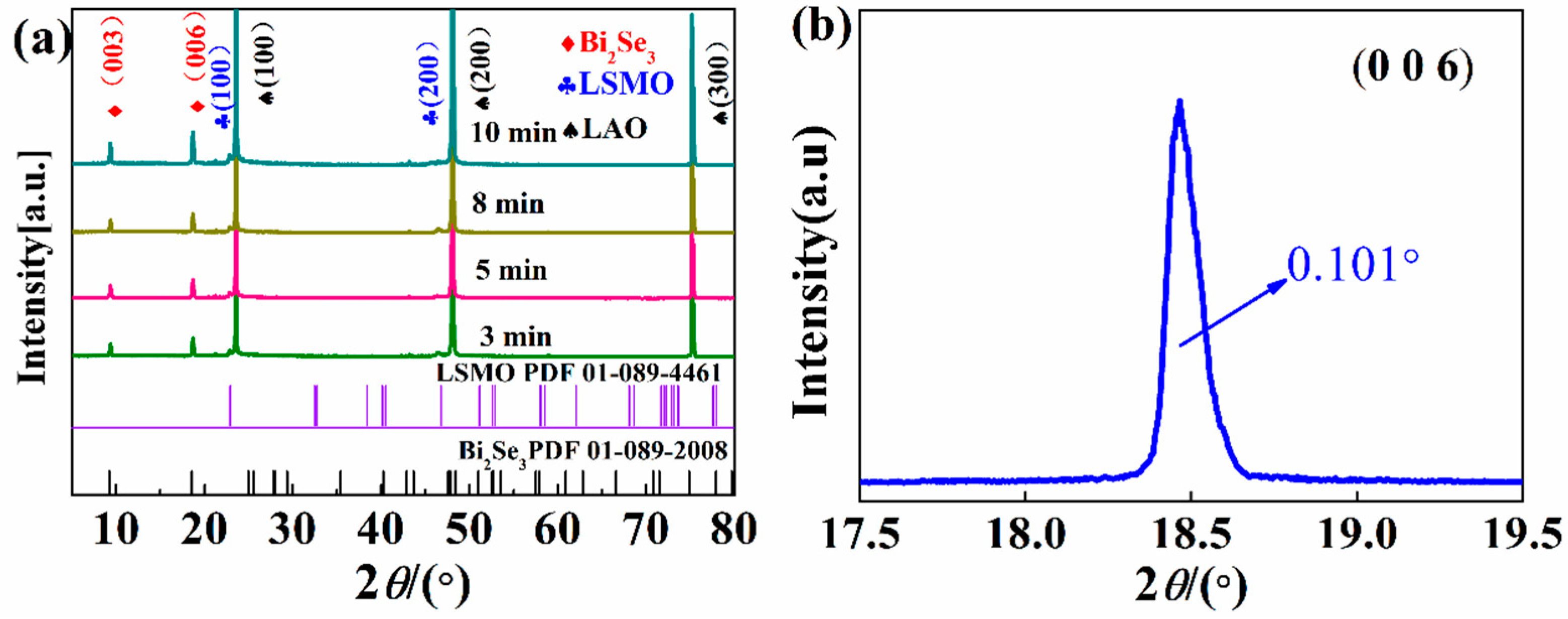
The three phases were observed in the spectrum as shown in Figure 1a, including Bi2Se3, LSMO and LAO (100). The Bi2Se3/LSMO thin films were based on LAO (100), so the XRD diffraction peak showed a strong LAO peak. LSMO had an a-axis orientation with (100) family peaks. The Bi2Se3 films showed (0 0 3n) reflection in the scanning range of 5°~80°, indicating that the film has high crystallinity along the growth direction [25]. Figure 1b shows the X-ray rocking curve of the Bi2Se3 sample (006) peak with deposition time t = 8 min. The diffraction peak was sharp and symmetrical, and the FWHM was 0.101°. The relative intensity of Bi2Se3/LSMO increased slightly with the increase of deposition time of Bi2Se3 films. Moreover, the XRD spectra of all samples were similar, indicating that the crystal quality of Bi2Se3 and the uniformity of thin films can be well reproduced on LSMO/LAO (001).
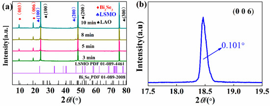
Figure 1.
(a) X-ray diffraction spectra of Bi2Se3 films on LaSrMnO3/LAO with different deposition times. (b) X-ray rocking curve of the (006) peak of the Bi2Se3 film of 8 min.
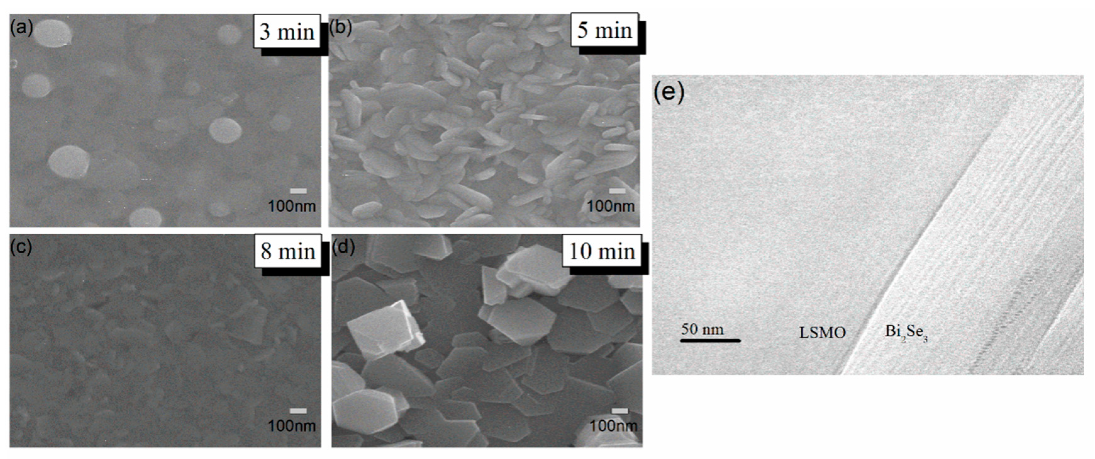
To study the influence of different deposition times on the morphology of thin films, the surface of the Bi2Se3 films was scanned through the SEM technique. Figure 2a–d shows the SEM images of Bi2Se3 films deposited on LSMO/LAO substrates with different deposition times, which ranged from 3 min to over 10 min. The films consisted of continuous nanosheets, with no cracks and voids. The surface of the sample deposited for 3 min was flat, which had some very small particles. With the increase of deposition time, these particles gradually formed a flake structure. The hexagonal structure was obviously observed in the sample with t = 10 min. The layered structure and hexagonal structure in the sample were clearly observed, in agreement with the XRD analysis [26,27]. For the Bi2Se3 films on LSMO/LAO with a different deposition time, the relative atomic ratio of Se/Bi was in the range of 1.43 to 1.47, which was lower than the nominal ratio of 1.5 in EDX results, as shown in Table 1. It is assumed that a small amount of Se vacancy occurred in the films. Figure 2e shows the TEM of the Bi2Se3/LSMO heterojunction with t = 8 min. The layered structure of Bi2Se3 can be clearly observed. The interface of Bi2Se3/LSMO has clear boundaries with no transitional region, which indicates that there is no obvious diffusion or chemical reaction between Bi2Se3 and LSMO.
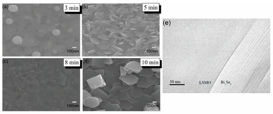
Figure 2.
(a–d) FESEM image of typical Bi2Se3 films grown on an LSMO/LAO substrate. (e) TEM images of Bi2Se3/LSMO/LAO with t = 8 min.

Table 1.
The EDX and thickness results of the Bi2Se3 films with deposition time.
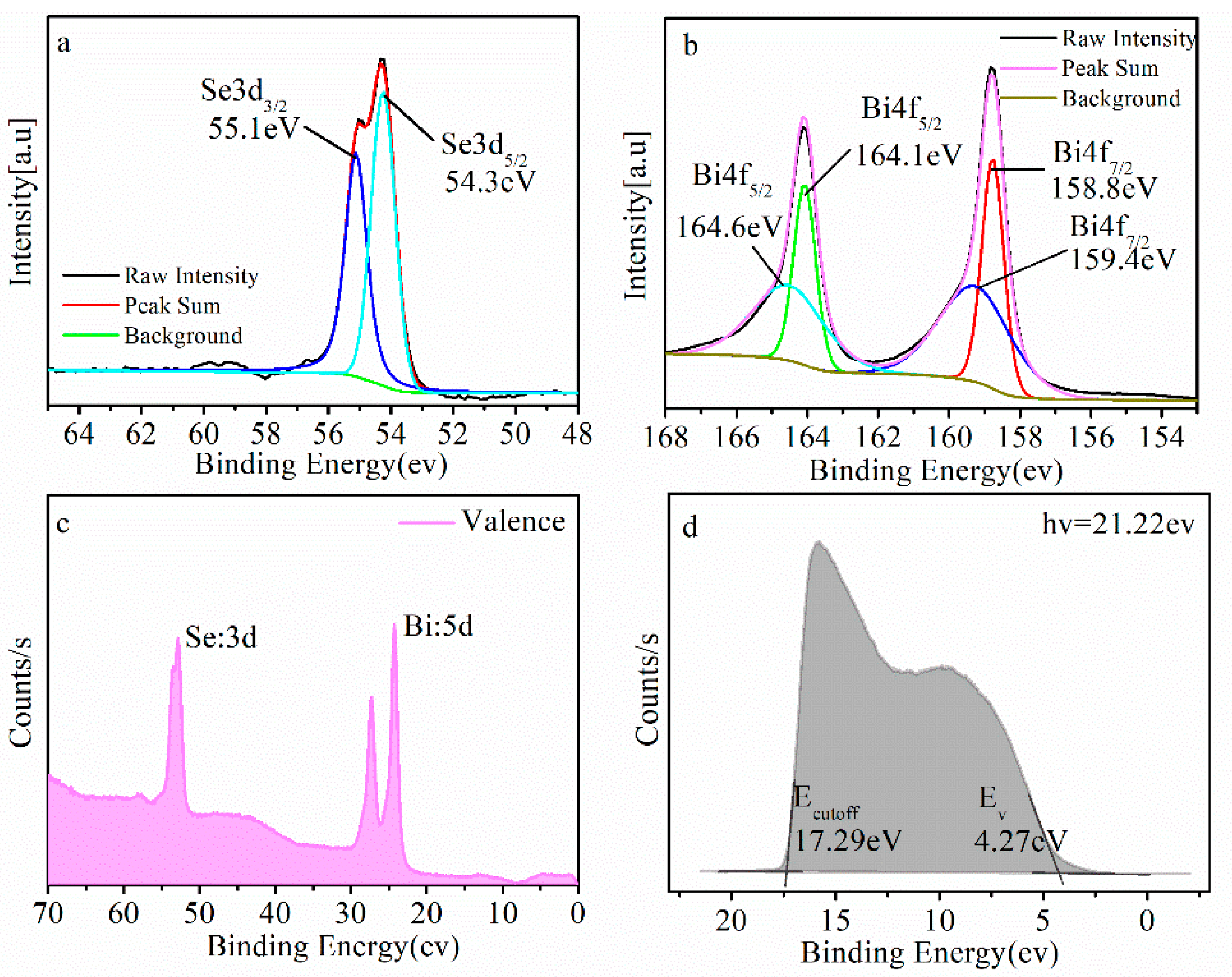
The XPS and UPS analysis of the spectrum are shown in Figure 3. C 1’s peak is often used for binding energy referencing in XPS by using the calibration method based on C 1’s peak position, and work function, : [28]. The value for C 1’s peak after calibration was 285.65 eV. The binding energies of Se and Bi were calibrated by 285.65 eV, as shown in Figure 3a,b.
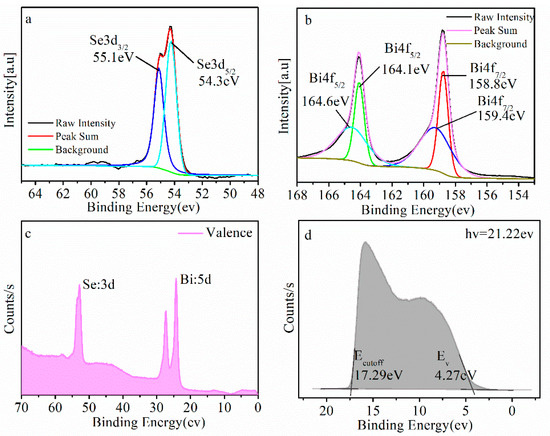
Figure 3.
XPS analysis of Bi2Se3/LSMO/LAO with t = 8 min; (a) the Se 3d peaks; (b) the Bi 4f peaks. (c) Valence-level measurements on Bi2Se3/LSMO/LAO taken with 100 eV photons. (d) UPS spectra of Bi2Se3/LSMO/LAO.
Figure 3a is the spectral fitting result of Se 3d, where the Se 3d5/2 and Se3d3/2 peaks were at 54.3 and 55.1 eV, respectively. The difference between the peaks of the Se3d peak was 0.8 eV, indicating that the valence state of Se in the Bi2Se3 was Se2-. There was a weak peak in the binding energy range of 57–60 eV, indicating that the Se–O bond (58.8 and 59.9 eV) appeared in the sample, suggesting that part of the sample was oxidized during storage. The peak in Figure 3b corresponded to the Bi 4d, with binding energy Bi 4f7/2 and Bi 4f5/2 being at 158.8 and 164.1 eV, respectively. The difference between the peaks of Bi 4f was 5.3 eV, which is completely consistent with the Bi3+, corresponding to the Bi–Se bond. The shoulder peaks Bi 4f7/2 (A) and Bi 4f5/2 (A) were found on the right side of the high binding energy, and the binding energies were 159.4 and 164.6 eV, respectively, indicating that the sample was oxidized during placement and that the Bi-O bond appeared. The surface composition ρSe/Bi = 1.49 could be estimated from the integrated peak intensity, which was close to the results of EDX and normally stoichiometry. Core-level spectroscopy was performed with 50 eV photons, with the samples held at room temperature. Figure 3c displays 3d and 5d valence levels (spin-orbit split doublets) of Se and Bi, respectively. The values of 5d5/2 and 5d3/2 were 24.3 and 27.5 eV. The peak of Se 3d was 52.9 eV. The fact that no extra peaks were observed indicates a good surface quality with a stoichiometric composition [29]. Figure 3d is the work function (ϕ) of the sample. The value of ϕ was measured to be 3.93 eV, which was smaller than the reported value [30]. The lower work function of our sample may be related to the thickness of the sample and the environment. The work function of layered Bi2Se3 is smaller than that of bulk Bi2Se3 [31]. The work function of Bi2Se3 samples decreased from 5.4 to 4.0 eV after air exposure [32]. Other factors could also have reduced work function of the sample, such as adsorption of other elements (Cesium) [33].
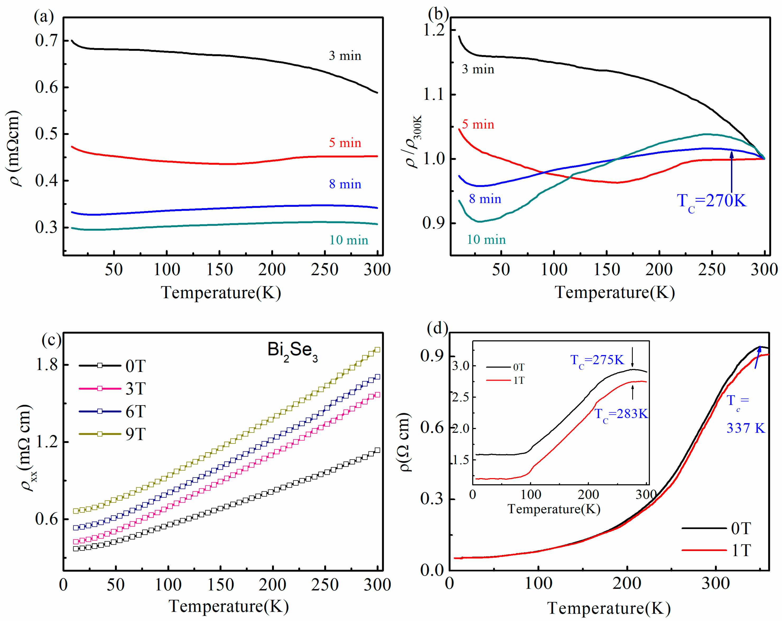
The resistivity in the ab plane of Bi2Se3/LSMO/LAO thin films with different deposition times was measured in the range of 2 K ≤ T ≤ 300 K at the zero field, as shown in Figure 4a. The electrical current was applied in the ab plane, and B was perpendicular to the ab plane. The resistivity of the sample decreased with the increase of Bi2Se3 deposition time. In the temperature range below 30 K, there was an insulator transition in all Bi2Se3/LSMO/LAO thin films, that is, the resistivity decreased with the increase of temperature, as shown in Figure 4b, revealing that an insulating state was attributed to the presence of an impurity band [29,34]. This is the conventional electrical transport characteristic of Bi2Se3 films [35]. The behavior of rising resistance indicates that it was due to the bulk carrier freezing of Bi2Se3. The carrier in surface states and impurity transitions of Bi2Se3 mainly causes the transport behavior [36]. The variation trend of the resistivity below 30 K was basically consistent with that of Fe-doped Bi2Se3 samples [37,38].
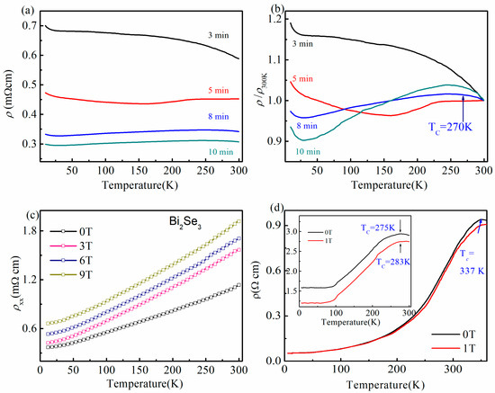
Figure 4.
(a) Temperature dependence of resistivity of Bi2Se3/LSMO/LAO thin films deposited at different times at the zero field. (b) Resistivity normalization curve for Bi2Se3/LSMO/LAO thin films with different deposition times at th zero field. (c) Temperature-dependent resistivity for Bi2Se3/LAO thin films with different magnetic fields. (d) Temperature dependence of resistivity for LSMO/LAO thin films in 0 T and 1 T magnetic field. Inset: Temperature dependence of resistivity for polymer LSMO/Si films.
The Bi2Se3 samples with deposition time t = 3 min exhibited complete insulation behavior in the whole measured temperature range, which was likely due to much stronger scattering from disorder and porosity [39]. These three samples (t ≥ 5 min) showed a metallic R vs T due to the existence of Se vacancies, as shown in Figure 4b [29]. For the t = 5 min, the metal insulation transition behavior began to appear at about 170 K. When t ≥ 8 min, with the decrease of temperature, the resistance increased at first, reached the maximum at about 270 K, and then decreased. The difference of sample resistance behavior is related to different deposition times of Bi2Se3 and intrinsic transport properties of Bi2Se3 and LSMO [40].
Figure 4c shows that the resistivity of pure Bi2Se3 thin films varied with temperature (ρ-T) between 300 and 5 K under different applied magnetic fields. Bi2Se3 thin films exhibited weak metal behavior, and their resistivity increased with the increase of the magnetic field [38]. The resistivity of LSMO/LAO thin films was 103-times higher than that of Bi2Se3 thin films, indicating that LSMO acts as the insulating substrate of Bi2Se3. Resistance peaks of LSMO/LAO films were observed when the transition temperature was 340 K at 0 T in Figure 4d. LSMO is a spin-polarized material with a perovskite structure and intrinsic insulator-metal (I-M) transition [41].
The TI-M of textured LSMO/LAO and single crystal is in the range of 340 to 360 K [42], which is close to the transition temperature of our LSMO/LAO samples. In order to compare the TI-M of polycrystalline LSMO films, non-textured LSMO/Si films were prepared. In polycrystalline and non-textured LSMO systems, the TI-M decreased to 275 K at 0 T, shown in the inset of Figure 4d. The value of the TI-M for LSMO/Si thin films was lower than that of LSMO/LAO thin films, which was due to the increase of spin scattering caused by more disorder in the grain boundary region in Si substrates [43].
For the Bi2Se3/LSMO/LAO thin films with t ≥ 8 min, the resistivity peak temperature of the Bi2Se3/LSMO/LAO film was about the same as that of the LSMO/Si film, about 270 K. The interface scattering [44] between the lower surface of Bi2Se3 and the upper surface of LSMO led to a scattering increase in the heterostructure, resulting in the decrease of TC of Bi2Se3/LSMO from 340 to 270 K. This characteristic may be attributed to the interaction between the ferromagnetic insulator and Bi2Se3 due to the proximity effect.
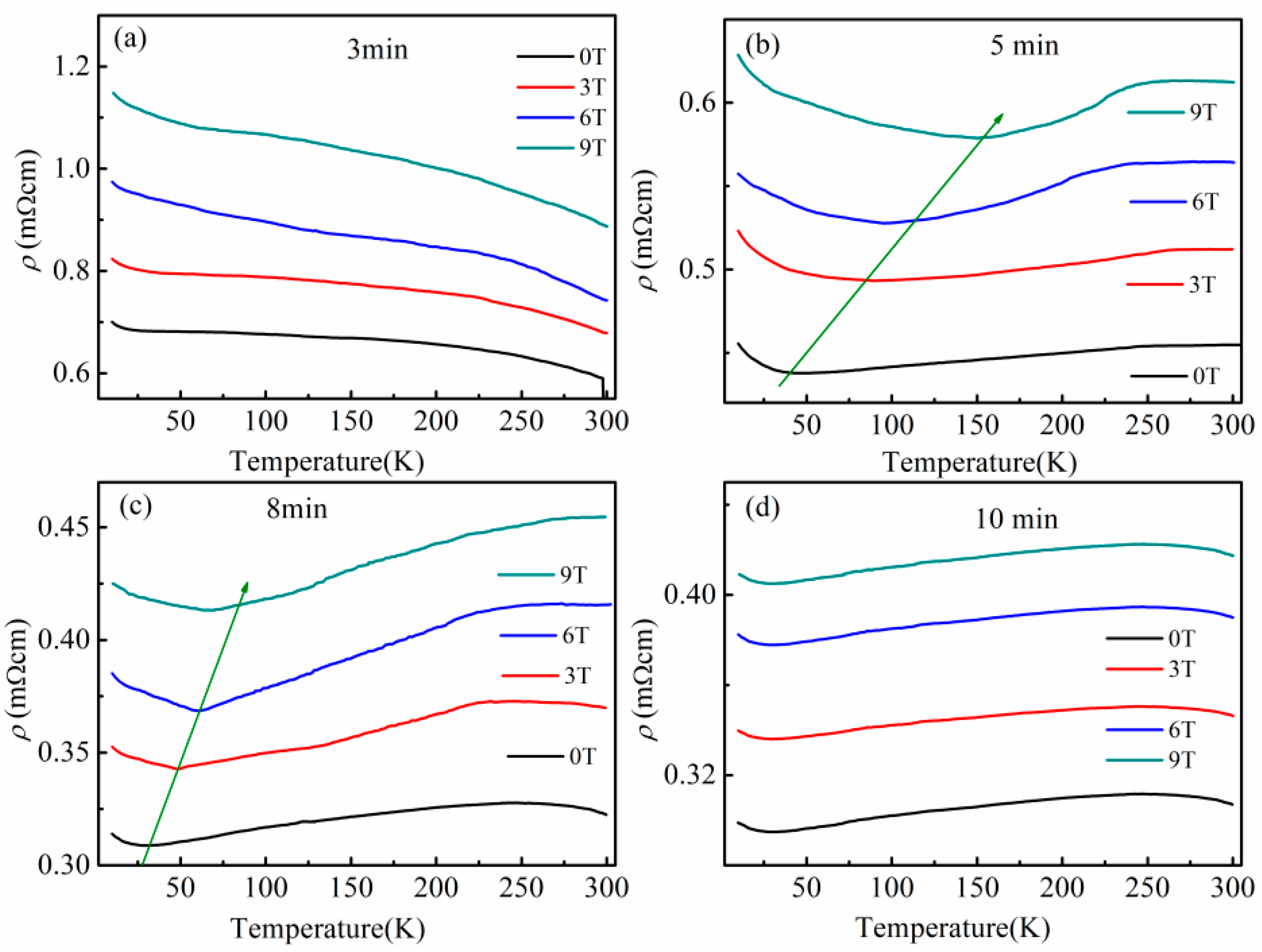
Figure 5 displays p-T curves of Bi2Se3/LSMO/LAO thin films under different applied fields from 0 to 9 T. The resistivity of all samples exhibits positive magnetoresistance (MR = ((pH − p0)/p0 × 100%). The sample with t = 3 min showed insulated resistivity. For the samples of t = 8 min and t = 10 min, the resistivity peak was found above 250 K, which is close to the metal-insulator transition temperature of LSMO [41]. This may be related to the intrinsic resistance peak of the LSMO. After reaching a maximum, the resistivity showed a metallic behavior between 30 and 270 K. The metallic resistivity indicates that phonon scattering was dominant in this temperature range.
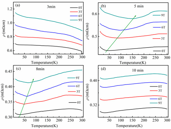
Figure 5.
The resistivity of Bi2Se3/LSMO/LAO deposited at different times varies with temperature at different applied fields: (a) 3 min; (b) 5 min; (c) 8 min; (d) 10 min.
For the thin films with t = 5 min, the resistivity was almost independent of temperature above 250 K. No resistance peak was found. The strong coupling and competition between LSMO and Bi2Se3 carriers led to the appearance and disappearance of intrinsic resistance peaks of LSMO [40]. A plausible mechanism for the resistivity characteristic may be attributed to the proximity effect, which leads to a spin injection from LSMO to Bi2Se3. The thickness of the Bi2Se3 layers was measured in the range of 53–710 nm, and the spin-diffusion length can be longer than 100 nm, as reported in ferromagnet-superconductor heterostructures [42,45], so the spin injection is considered to be a long-range interaction of the proximity effect. Compared with local short-range interaction, spin injection is non-localized. The magnetic field drives the LSMO layer from a highly disordered multiple domain model into a state of uniform magnetization, which considerably reduces the spin flip scattering on the interface and increases the efficiency of spin injection. The spin polarized quasi-particles diffuse into Bi2Se3, which plays an important role in controlling the transport properties [40].
Below 250 K, the electrical resistance decreases with the decrease of temperature. With decreasing temperature, the resistivity decreases, reaching a minimum. Then, the resistivity increases below the transition temperature Tmin. As the magnetic field increases, Tmin moves to a high temperature, shown in of Figure 5b,c, which manifests that the magnetic field has a great influence on the total conductivity.
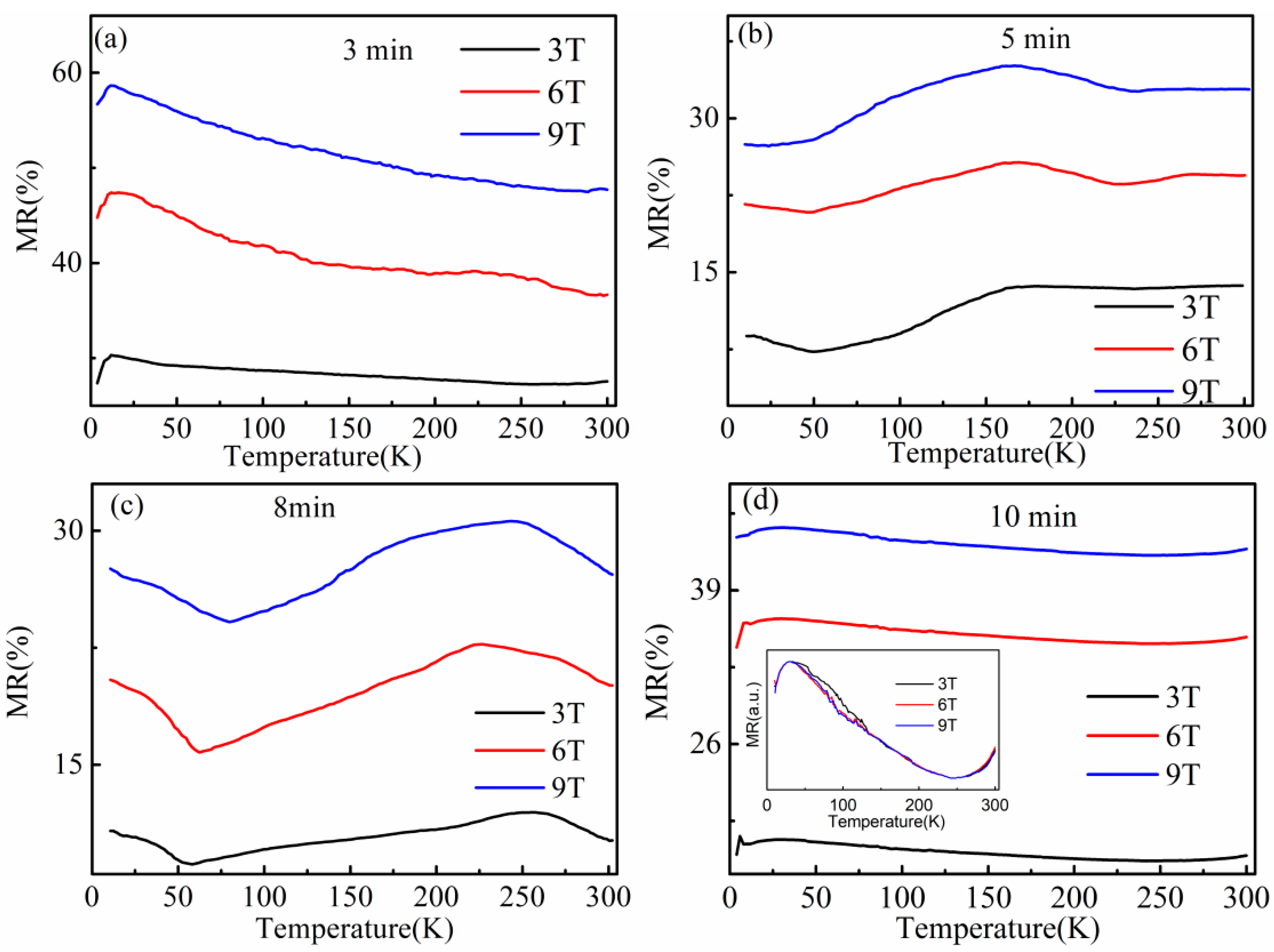
Figure 6 shows the magnetoresistance ratio (MR%) of the Bi2Se3/LSMO/LAO thin films versus temperature. Here, the resistivity changed, caused by the extra magnetic field, and the rate of change is called magnetoresistance. Changes in MR showed almost the same trend in Figure 6a,d. Magnetoresistance peaks appeared at about 30 K. The simultaneous reversal of ρ(T) and MR-T properties was observed at a low temperature of about 30 K, which indicates that the SSs contributions of Bi2Se3 were significantly improved upon due to the LSMO film [37]. Figure 6b,c shows a similar trend. With the increase of temperature, the MR first decreased, then increased to the maximum value near 270 K and then decreased. The changing trend of MR in different temperature ranges reflects the competition between MR of LSMO and Bi2Se3 [40]. It is reasonable to assume that the electrical transport mechanisms of LSMO and Bi2Se3 are different. Below 30 K, the conductance is mainly contributed by surface state carriers, which shows the electrical transport characteristics of Bi2Se3, while LSMO conductance dominates at high-temperature regions due to the emergence of MR peaks and the resistance peak.
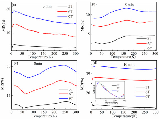
Figure 6.
Temperature-dependent magnetoresistance (MR) ratio of Bi2Se3/LSMO/LAO thin films under different applied magnetic fields: (a) 3 min; (b) 5 min; (c) 8 min; (d) 10 min. Inset in (d): The relationship between the relative resistivity and T below 30 K.
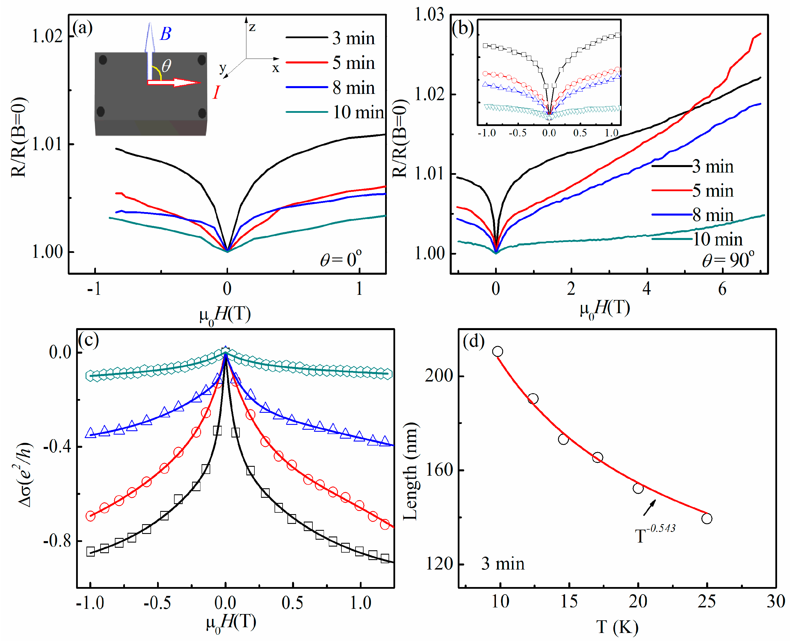
Figure 7 shows the resistivity versus applied field measured at 10 K. In MR measurements, θ represents the angle between the B field and the current I and the B field in the z direction and the Hall voltage probes in the y direction, as shown in Figure 7a. In Figure 7b, an unsaturated MR appears under a high applied magnetic field, which is associated with topological surface states [46]. A WAL cusp comes from the spin-momentum locked surface states [47], which is consistent with a recent transport study in Bi2Se3 films [19,48]. The WAL cusp is most pronounced at t = 3 min, and it becomes weaker gradually with the increase of the deposition time. The low field MR of topological insulators shows that the shorter the t is, the more obvious the WAL effect is, which is related to the thickness of the thin film. When the B is parallel to the plane (θ = 0°), the 2D WAL effect disappears [49], and the 3D WAL effect derived from the bulk channel can be observed in the sample in Figure 7a. When the B is perpendicular to the plane (θ = 90°), it can be ascribed to 2D and 3D WAL. The 2D WAL effect can be obtained by deducting the 3D WAL effect.
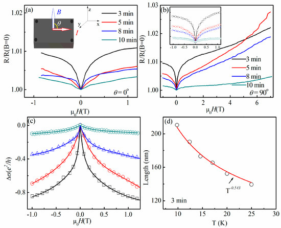
Figure 7.
(a) Normalized magnetoresistance of Bi2Se3 films on LSMO/LAO of different deposition times measured at θ = 0°, T = 10 K. (b) Normalized magnetoresistance of Bi2Se3 films measured at θ = 90°, T = 10 K. Inset: enlarged view of MR near zero fields showing the robustness of the WAL effect. (c) The HLN fit of the weak-field magnetoconductivity Δσ for films with different deposition times measured at T = 10 K after subtracting the 3D bulk contribution; solid curves represent fitting data. (d) The relationship between the coherence length of t = 3 min Bi2Se3 film and temperature. The circle represents the experimental results, and the solid curve represents the fitting results.
Using the resistivity of the Figure 7a,b, tge 2D magnetoconductivity Δσ can be evaluated with the Hikami–Larkin–Nagaoka (HLN) formalism [50], as shown in Figure 6c.
where e, h, lϕ, Ψ and α are the electronic charge, the Planck’s constant, phase coherent length, digamma function and a coefficient, respectively. Bϕ = h/4elϕ2. α is −0.5 for one topological surface and −1 in a film with both upper and lower surfaces [49,51]. The information of lϕ and α is obtained by data fitting, which is listed in Table 2. The value of α was −0.34 and −0.43, which is consistent with the case of α = −0.5, indicating that only one surface channel contributed to the 2D WAL effect. The value of α was −0.61 and −0.69, which indicates that there was a small part of coupling between the upper and lower channels of Bi2Se3 films, and the remaining part was mainly one channel [52]. lϕ increased steadily with deposition time from lϕ ≈ 210 nm to lϕ ≈ 517 nm at 10 K, which was close to the value of lϕ~500 nm estimated from the Bi2Se3 nanoribbons [53]. The phase coherence length lϕ can be obtained from Bϕ = h/4elϕ2, in which the coherence length lϕ monotonically increases as the samples get thicker [54]. There is allometric behavior with lϕ∝T−0.543 between lϕ values and temperature. Theoretically, the system is two dimensional when lϕ∝T−1/2 [55]. The exponent was very close to the expected −1/2, indicating that the Bi2Se3 film (t = 3 min) is a two-dimensional system. The lφ of the Bi2Se3/LAO sample was 457 nm, which is larger than that of the magnetic sample Bi2Se3/LSMO/LAO (t = 3, 5, 8 min). The lφ of the Bi2Se3/LSMO/LAO decreased obviously, indicating that the magnetic proximity coupling suppressed the WAL effect [19,56]. The electron cancellation interference caused by spin-orbit coupling could be destroyed by magnetic scattering or by an external magnetic field, resulting in the decrease of lφ.
Table 2.
Lists of Bi2Se3 films with different deposition times and fitting parameters of the lϕ and the α.
Figure 8 shows magnetization versus applied magnetic field curves for the bilayer films Bi2Se3/LSMO. The Bi2Se3/LAO film was diamagnetic, consistent with previous reports, as shown in Figure 8a [57]. The magnetization at 10 K for Bi2Se3/LSMO films had obvious saturation and hysteresis that are shown in Figure 8b, which are evidence of ferromagnetic signals. The coercive field Hc = 105 Oe for Bi2Se3/LAO film. The magnetization data also confirmed that magnetism was induced in Bi2Se3 films. Figure 8c draws the magnetic hysteresis loops of Bi2Se3 film on LSMO/LAO measured at 10 K. There were obvious hysteresis loops in the Bi2Se3/LSMO/LAO substrates, indicating the existence of ferromagnetic states in the films. The coercive field Hc = 726 Oe for t = 3 min sample, Hc = 315 Oe for t = 5 min sample, Hc = 279 Oe for t = 8 min sample and Hc = 252 Oe for t = 10 min sample, decreasing as the deposition time increased. The coercive field of Bi2Se3/LSMO/LAO was slightly larger than that of LSMO/LAO, which could be attributed to interface exchange coupling [58]. The saturated total magnetic moment of Bi2Se3/LSMO samples (8 min) was about 27% higher than that of LSMO/LAO samples, as shown in Figure 8b,c, which indicates that additional induced magnetic moments were generated in heterojunctions through short-range ferromagnetic exchange at the interface [59]. The short-range proximity effect between LSMO and Bi2Se3 mainly comes from charge transfer and redistribution, orbital hybridization and exchange coupling [19,59]. The characteristic scales of effects are generally under 10 nm due to the localization [45]. The field-cooled magnetization curve for Bi2Se3/LSMO samples is shown in Figure 8d. It can be further proved that magnetism was induced in Bi2Se3. The Curie temperature of the LSMO/LAO film was around 350 K, while the Curie temperature of t = 5 min Bi2Se3/LSMO sample was about 270 K. Below 270 K, the rapid increase of magnetization M of Bi2Se3/LSMO/LAO with the decrease of temperature T was caused by ferromagnetic phase transition, which is consistent with the LSMO film itself. Above 270 K, M was larger than that of LSMO, indicating there were some amounts of magnetic moments induced in the Bi2Se3/LSMO/LAO heterostructure.
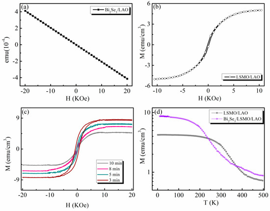
Figure 8.
Hysteresis curves measured at 10 K with an in-plane applied field: (a) the Bi2Se3/LAO films, (b) the LSMO/LAO films measured, (c) the Bi2Se3/LSMO/LAO films. (d) Magnetization versus temperature of Bi2Se3 film on LSMO/LAO measured during field cooling with 1 kOe.
4. Conclusions
Topological insulator Bi2Se3 thin films were prepared on LSMO/LAO substrates by magnetron sputtering. The magnetic characterization and electrical and magnetic transport properties of the new TI/FM heterostructure were studied. The transport measurement showed that the conductance was mainly contributed by Bi2Se3 in the low temperature region (below 30 K), while LSMO conductance dominated at the high-temperature regions, which could be explained by the short-range interactions and long-range interaction. The short-range interactions were related to four mechanisms: charge transfer and redistribution, orbital hybridization, and exchange coupling. The long-range interaction was assumed to be associated with the spin injection. At a low magnetic field, MR showed a WAL spike. With the increase of deposition time, the WAL spike was gradually suppressed. The HLN quantum interference model can be used to fit the magnetic conductance under the low field data of 10 K. The WAL effect of Bi2Se3 was strongly suppressed by the induced magnetism. The additional induced moments and suppressed WAL effect proved the emergence of a ferromagnetic phase in Bi2Se3 films. We conclude that ferromagnetism in LSMO films affects the Bi2Se3 thin film. This indicates that the ferromagnetic order may be introduced into the Bi2Se3 film due to the magnetic proximity effect of the LSMO. Our results on a TI/FMI heterostructure provide a way for the study of proximity-induced magnetism in TIS and the application of TI-based spintronic devices.
Author Contributions
Methodology, M.Z.; validation, M.Z., and Q.L.; formal analysis, M.Z. and L.L.; investigation, M.Z., T.Z.; resources, M.Z., T.Z.; data curation, M.Z.; writing—original draft preparation, M.Z.; writing—review and editing, M.Z., Q.L., L.L. and T.Z.; funding acquisition, M.Z. All authors have read and agreed to the published version of the manuscript.
Funding
The research was supported by the National Natural Science Foundation of China (Grant No.11804281) and the Fund Project of the Ministry of Education of China (No. Z2017093).
Institutional Review Board Statement
Not applicable.
Informed Consent Statement
Not applicable.
Data Availability Statement
Not applicable.
Conflicts of Interest
The authors declare no conflict of interest.
References
- Xia, Y.; Qian, D.; Hsieh, D.; Wray, L.; Pal, A.; Lin, H.; Bansil, A.; Grauer, D.; Hor, Y.S.; Cava, R.J.; et al. Discovery (theoretical prediction and experimental observation) of a large-gap topological-insulator class with spin-polarized single-Dirac-cone on the surface. Nat. Phys. 2009, 5, 398–402. [Google Scholar] [CrossRef] [Green Version]
- Chang, C.Z.; Zhang, J.S.; Feng, X.; Shen, J.; Zhang, Z.C.; Guo, M.H.; Li, K.; Ou, Y.B.; Wei, P.; Wang, L.L.; et al. Experimental Observation of the Quantum Anomalous Hall Effect in a Magnetic Topological Insulator. Science 2013, 340, 167–170. [Google Scholar] [CrossRef] [PubMed] [Green Version]
- Qi, X.L.; Zhang, S.C. The quantum spin Hall effect and topological insulators. Phys. Today 2010, 63, 33–38. [Google Scholar] [CrossRef] [Green Version]
- Wang, M.X.; Liu, C.; Xu, J.P.; Fang, Y.; Lin, M.; Yao, M.Y.; Gao, C.L.; Shen, C.Y.; Ma, X.C.; Chen, X.; et al. The coexistence of superconductivity and topological order in the Bi2Se3 thin films. Science 2012, 336, 52–55. [Google Scholar] [CrossRef]
- Chang, C.Z.; Wei, P.; Moodera, J.S. Breaking time reversal symmetry in topological insulators. MRS Bull. 2014, 39, 867–872. [Google Scholar] [CrossRef] [Green Version]
- Li, M.D.; Cui, W.P.; Yu, J.; Dai, Z.Y.; Wang, Z.; Katmis, F.; Guo, W.L.; Moodera, J. Magnetic proximity effect and interlayer exchange coupling of ferromagnetic/topological insulator/ferromagnetic trilayer. Phys. Rev. B 2015, 91, 014427. [Google Scholar] [CrossRef] [Green Version]
- Zheng, G.L.; Wang, N.; Yang, J.Y.; Wang, W.K.; Du, H.F.; Ning, W.; Yang, Z.R.; Lu, H.Z.; Zhang, Y.H.; Tian, M.L. Weak localization effect in topological insulator micro flakes grown on insulating ferrimagnet BaFe12O19. Sci. Rep. 2016, 6, 21334. [Google Scholar] [CrossRef] [Green Version]
- Zhang, Z.; Feng, X.; Wang, J.; Lian, B.; Zhang, J.; Chang, C.; Guo, M.; Ou, Y.; Feng, Y.; Zhang, S.C.; et al. Magnetic quantum phase transition in Cr-doped Bi2(SexTe1−x)3 driven by the Stark effect. Nat. Nanotechnol. 2017, 12, 953–957. [Google Scholar] [CrossRef] [Green Version]
- Wei, P.; Katmis, F.; Assaf, B.A.; Steinberg, H.; Herrero, P.J.; Heiman, D.; Moodera, J.S. Exchange-Coupling-Induced Symmetry Breaking in Topological Insulators. Phys. Rev. Lett. 2013, 110, 186807. [Google Scholar] [CrossRef]
- Zhang, M.; Liu, L.G.; Yang, H. Anomalous second ferromagnetic phase transition in Co0.08Bi1.92Se3 topological insulator. J. Alloy. Compd. 2016, 678, 463–467. [Google Scholar] [CrossRef]
- Yang, Q.I.; Dolev, M.; Zhang, L.; Zhao, J.F.; Fried, A.D.; Schemm, E.; Liu, M.; Palevski, A.; Marshall, A.F.; Risbud, S.H.; et al. Emerging Weak Localization Effects on Topological Insulator-Insulating Ferromagnet Bi2Se3-EuS Interface. Phys. Rev. B 2013, 88, 081407. [Google Scholar] [CrossRef] [Green Version]
- Liu, W.Q.; He, L.; Zhou, Y.; Murata, K.; Onbasli, M.C.; Ross, C.A.; Jiang, Y.; Wang, Y.; Xu, Y.B.; Zhang, R.; et al. Evidence for ferromagnetic coupling at the doped topological insulator/ferrimagnetic insulator interface. AIP Adv. 2016, 6, 055813. [Google Scholar] [CrossRef] [Green Version]
- Hu, Y. Prediction of reentering and switching ferromagnet/antiferromagnet exchange bias by antiferromagnetic proximity effect. Nanotechnology 2019, 30, 025708. [Google Scholar] [CrossRef] [PubMed]
- Casas, O.E.; Arrachea, L.; Herrera, W.J.; Yeyati, A.L. Proximity Induced Time-Reversal Topological Superconductivity in Bi2Se3 Films without Phase Tuning. Phys. Rev. B 2019, 99, 161301. [Google Scholar] [CrossRef] [Green Version]
- Dai, W.Q.; Richardella, A.; Du, R.Z.; Zhao, W.W.; Liu, X.; Liu, C.X.; Huang, S.H.; Sankar, R.; Chou, F.C.; Samarth, N.; et al. Proximity-Effect-Induced Superconducting Gap in Topological Surface States-A Point Contact Spectroscopy Study of NbSe2/Bi2Se3 Superconductor-Topological Insulator Heterostructures. Sci. Rep. 2017, 7, 7631. [Google Scholar] [CrossRef] [Green Version]
- Dmytro, P.; MacDonald, A.H. Spintronics and Pseudospintronics in Graphene and Topological Insulators. Nat. Mater. 2012, 11, 409–416. [Google Scholar]
- Lang, M.R.; Montazeri, M.; Onbasli, M.C.; Kou, X.F.; Fan, Y.B.; Upadhyaya, P.; Yao, K.Y.; Liu, F.; Jiang, Y.; Jiang, W.J.; et al. Proximity Induced High-Temperature Magnetic Order in Topological Insulator-Ferrimagnetic Insulator Heterostructure. Nano Lett. 2014, 14, 3459–3465. [Google Scholar] [CrossRef]
- Eremeev, S.V.; Otrokov, M.M.; Chulkov, E.V. New universal type of interface in the magnetic insulator/topological insulator heterostructures. Nano Lett. 2018, 18, 6521–6529. [Google Scholar] [CrossRef]
- Zhu, S.N.; Meng, D.C.; Liang, G.H.; Shi, G.; Zhao, P.; Cheng, P.; Li, Y.Q.; Zhai, X.F.; Lu, Y.L.; Chen, L.; et al. Proximity-Induced Magnetism and an Anomalous Hall Effect in Bi2Se3/LaCoO3: A Topological Insulator/Ferromagnetic Insulator Thin Film Heterostructure. Nanoscale 2018, 10, 10041–10049. [Google Scholar] [CrossRef]
- Kandala, A.; Richardella, A.; Rench, D.W.; Zhang, D.M.; Flanagan, T.C.; Samarth, N. Growth and Characterization of Hybrid Insulating Ferromagnet-Topological Insulator Heterostructure Devices. Appl. Phys. Lett. 2013, 103, 202409. [Google Scholar] [CrossRef] [Green Version]
- Haghiri-Gosnet, A.M.; Renard, J.P. CMR manganites: Physics, thin films and devices. J. Phys. D Appl. Phys. 2003, 36, R127. [Google Scholar] [CrossRef]
- Zhao, X.; Wong, H.F.; Liu, Y.K.; Ng, S.M.; Cheng, W.F.; Mak, C.L.; Leung, C.W. Exchange bias effect in epitaxial La0.35Sr0.65MnO3/La0.7Sr0.3MnO3 bilayers: Impact of antiferromagnet growth conditions. Vacuum 2020, 175, 109280. [Google Scholar] [CrossRef]
- Mlack, J.T.; Rahman, A.; Johns, G.L.; Livi, K.J.T.; Marković, N. Substrate-independent catalyst-free synthesis of high-purity Bi2Se3 nanostructures. Appl. Phys. Lett. 2013, 102, 193108. [Google Scholar] [CrossRef] [Green Version]
- Liu, Q.; Zhang, M.; Song, T. Transport properties of La0.7Sr0.3MnO3/Si thin films grown by polymer-assisted chemical solution deposition. J. Synth. Cryst. 2017, 46, 621–626. [Google Scholar] [CrossRef]
- Vicente, C.P.; Tirado, J.L.; Adouby, K.; Jumas, J.C.; Touré, A.A.; Kra, G. X-ray Diffraction and 119Sn Mössbauer Spectroscopy Study of a New Phase in the Bi2Se3−SnSe System: SnBi4Se7. Inorg. Chem. 1999, 38, 2131–2135. [Google Scholar] [CrossRef]
- Richardella, A.; Zhang, D.M.; Lee, J.S.; Koser, A.; Rench, D.W.; Yeats, A.L.; Buckley, B.B.; Awschalom, D.D.; Samarth, N. Coherent heteroepitaxy of Bi2Se3 on GaAs (111) B. Appl. Phys. Lett. 2010, 97, 262104. [Google Scholar] [CrossRef]
- Xie, M.H.; Seutter, S.M.; Zhu, W.K.; Zheng, L.X.; Wu, H.; Tong, S.Y. Anisotropic Step-Flow Growth and Island Growth of GaN(0001) by Molecular Beam Epitaxy. Phys. Rev. Lett. 1999, 82, 2749. [Google Scholar] [CrossRef] [Green Version]
- Greczynski, G.; Hultman, L. Reliable determination of chemical state in X-ray photoelectron spectroscopy based on sample-work-function referencing to adventitious carbon: Resolving the myth of apparent constant binding energy of the C 1s peak. Appl. Sur. Sci. 2018, 451, 99–103. [Google Scholar] [CrossRef]
- Liang, H.; Xiu, F.; Wang, Y.; Fedorov, A.V.; Huang, G.; Kou, X.; Lang, M.; Beyermann, W.P.; Zou, J.; Wang, K.L. Epitaxial growth of Bi2Se3 topological insulator thin films on Si (111). J. Appl. Phys. 2011, 109, 103702. [Google Scholar]
- Kordyuk, A.A.; Kim, T.K.; Zabolotnyy, V.B.; Evtushinsky, D.V.; Bauch, M.; Hess, C.; Buchner, B.; Berger, H.; Borisenko, S.V. Photoemission-induced gating of topological insulators. Phys. Rev. B 2011, 83, 081303(R). [Google Scholar] [CrossRef] [Green Version]
- Huang, H.; Li, Y.; Qi, L.; Li, B.; Song, Z.; Huang, W.; Zhao, C.; Zhang, H.; Wen, S.; Carroll, D.; et al. Field electron emission of layered Bi2Se3 nanosheets with atom-thick sharp edges. Nanoscale 2014, 6, 8306–8310. [Google Scholar] [CrossRef] [PubMed]
- Edmonds, M.T.; Hellerstedt, J.T.; Tadich, A.; Schenk, A.; O’Donnell, K.M.; Tosado, J.; Butch, N.P.; Syers, P.; Paglione, J.; Fuhrer, M.S. Stability and Surface Reconstruction of Topological Insulator Bi2Se3 on Exposure to Atmosphere. J. Phys. Chem. C 2014, 118, 20413–20419. [Google Scholar] [CrossRef]
- Zhu, H.; Zhou, W.; Yarmoff, J.A. Cs adsorption on Bi2Se. Surf. Sci. 2019, 683, 17–22. [Google Scholar] [CrossRef]
- Zhang, M.; Wei, Z.; Jin, R.; Jia, Y.; Yan, Y.; Pu, X.; Yang, X.; Zhao, Y. Electrical transport properties and morphology of topological insulator Bi2Se3 thin films with different thickness prepared by magnetron sputtering. Thin Solid Film. 2016, 603, 289–293. [Google Scholar] [CrossRef]
- Li, M.Z.; Wang, Z.H.; Yang, L.; Pan, D.S.; Li, D.; Gao, X.P.; Zhang, Z.D. Growth and quantum transport properties of vertical Bi2Se3 nanoplate films on Si substrates. Nanotechnology 2018, 29, 315706. [Google Scholar] [CrossRef] [PubMed]
- Liu, M.H.; Chang, C.Z.; Zhang, Z.C.; Zhang, Y.; Ruan, W.; He, K.; Wang, L.L.; Chen, X.; Jia, J.F.; Zhang, S.C.; et al. Electron interaction-driven insulating ground state in Bi2Se3 topological insulators in the two-dimensional limit. Phys. Rev. B 2011, 83, 165440. [Google Scholar] [CrossRef] [Green Version]
- Chen, Y.L.; Chu, J.; Analytis, J.; Liu, Z.K.; Igarashi, K.; Kuo, H.; Qi, X.L.; Mo, S.K.; Moore, R.G.; Lu, D.H.; et al. Massive Dirac fermion on the surface of a magnetically doped topological insulator. Science 2010, 329, 659–662. [Google Scholar] [CrossRef] [Green Version]
- Lv, L.; Zhang, M.; Wei, Z.T.; Yang, L.Q.; Yang, X.S.; Zhao, Y. Enhanced contribution of surface state and modification of magnetoresistance in FexBi2-xSe3 topological insulator crystals. J. Appl. Phys. 2013, 113, 043923. [Google Scholar] [CrossRef]
- Borchmann, J.; Peregbarnea, T. Analytic expression for the entanglement entropy of a two-dimensional topological superconductor. Phys. Rev. B 2017, 95, 075152. [Google Scholar] [CrossRef] [Green Version]
- Yang, X.S.; Zhao, T.; Liu, Q.Y.; Zhao, K.; Wei, Z.T.; Zhao, Y. Transport properties for Bi2Se3/La0.7Sr0.3MnO3 composites. Ceram. Int. 2020, 46, 4748–4753. [Google Scholar] [CrossRef]
- Salamon, M.B.; Jaime, M. The physics of manganites: Structure and transport. Rev. Mod. Phys. 2001, 73, 583–628. [Google Scholar] [CrossRef]
- Lin, J.G.; Cheng, S.; Chang, C.; Xing, D.Y. Supercouducting and transport properties of YBa2Cu3O7/La0.7Sr0.3MnO3 bilayers. J. Appl. Phys. 2005, 98, 023910. [Google Scholar] [CrossRef]
- Liu, S.M.; Zhu, X.B.; Yang, J.; Song, W.H.; Dai, J.M.; Sun, Y.P. The effect of grain boundary on the properties of La0.7Sr0.3MnO3 thin films prepared by chemical solution deposition. Ceram. Int. 2006, 32, 157–162. [Google Scholar] [CrossRef]
- Lin, Y.B.; Huang, Z.G.; Yang, Y.M.; Wang, S.; Li, S.D.; Zhang, F.M.; Du, Y.W. Giant positive magnetoresistance in heterostructure (La0.7Sr0.3MnO3) coated with YBa2Cu3O7 composites. Appl. Phys. A 2011, 104, 143–147. [Google Scholar] [CrossRef]
- Habermeier, H.U. Ferromagnet-superconductor interfaces: The length scales of interactions. J. Phys. Conf. Ser. 2008, 108, 012039. [Google Scholar] [CrossRef]
- Tang, H.; Liang, D.; Qiu, R.L.J.; Gao, X.P.A. Two-Dimensional Transport-Induced Linear Magneto-Resistance in Topological Insulator Bi2Se3 Nanoribbons. ACS Nano 2011, 5, 7510–7516. [Google Scholar] [CrossRef] [Green Version]
- Checkelsky, J.G.; Hor, Y.S.; Liu, M.H.; Qu, D.X.; Cava, R.J.; Ong, N.P. Quantum interference in macroscopic crystals of nonmetallic Bi2Se3. Phys. Rev. Lett. 2009, 103, 246601. [Google Scholar] [CrossRef]
- Hattacharyya, B.; Sharma, A.; Sinha, B.B.; Shah, K.; Jejurikar, S.M.; Senguttuvan, T.D.; Husale, S. Evidence of Robust 2D Transport and Efros-Shklovskii Variable Range Hopping in Disordered Topological Insulator (Bi2Se3) Nanowires. Sci. Rep. 2017, 7, 7825. [Google Scholar] [CrossRef]
- He, H.T.; Wang, G.; Zhang, T.; Sou, I.K.; Wong, G.K.L.; Wang, J.N.; Lu, H.Z.; Shen, S.Q.; Zhang, F.C. Impurity Effect on Weak Antilocalization in the Topological Insulator Bi2Te3. Phys. Rev. Lett. 2011, 106, 166805. [Google Scholar] [CrossRef] [Green Version]
- Hikami, S.; Larkin, A.I.; Nagaoka, Y. Spin-Orbit Interaction and Magnetoresistance in the two Dimensional Random System. Prog. Theor. Phys. 1980, 63, 707–710. [Google Scholar] [CrossRef]
- Lee, Y.F.; Kumar, R.; Hunte, F.; Narayan, J.; Schwartz, J. Microstructure and transport properties of epitaxial topological insulator Bi2Se3 thin films grown on MgO (100), Cr2O3 (0001), and Al2O3 (0001) templates. J. Appl. Phys. 2015, 118, 125309. [Google Scholar] [CrossRef]
- Steinberg, H.; Laloë, J.B.; Fatemi, V.; Moodera, J.S.; Herrero, P.J. Electrically tunable surface-to-bulk coherent coupling in topological insulator thin films. Phys. Rev. B 2011, 84, 233101. [Google Scholar] [CrossRef] [Green Version]
- Yong, S.K.; Brahlek, M.; Bansal, N.; Edrey, E.; Kapilevich, G.A.; Iida, K.; Tanimura, M.; Horibe, Y.; Cheong, S.W.; Oh, S. Thickness-dependent bulk properties and weak antilocalization effect in topological insulator Bi2Se3. Phys. Rev. B 2011, 84, 073109. [Google Scholar]
- Altshuler, B.L.; Aronov, A.G.; Khmelnitskii, D.E. Effects of electron-electron collisions with small energy transfers on quantum localization. J. Phys. C Solid State Phys. 1982, 15, 7367. [Google Scholar] [CrossRef]
- Che, X.Y.; Murata, K.; Pan, L.; He, Q.L.; Yu, G.Q.; Shao, Q.M.; Yin, G.; Deng, P.; Fan, Y.B.; Ma, B.; et al. Proximity-Induced Magnetic Order in a Transferred Topological Insulator Thin Film on a Magnetic Insulator. ACS Nano 2018, 12, 5042–5050. [Google Scholar] [CrossRef] [PubMed]
- Li, H.; Song, Y.R.; Yao, M.Y.; Zhu, F.; Liu, C.; Gao, C.L.; Jia, J.F.; Qian, D.; Yao, X.; Shi, Y.J.; et al. Carrier density dependence of the magnetic properties in iron-doped Bi2Se3 topological insulator. J. Appl. Phys. 2013, 113, 043926. [Google Scholar] [CrossRef] [Green Version]
- Manna, P.K.; Yusuf, S.M. Two interface effects: Exchange bias and magnetic proximity. Phys. Rep. 2014, 535, 61–69. [Google Scholar] [CrossRef]
- Katmis, F.; Lauter, V.; Nogueira, F.S.; Assaf, B.A.; Jamer, M.E.; Wei, P.; Satpati, B.; Freeland, J.W.; Eremin, I.; Heiman, D.; et al. A high-temperature ferromagnetic topological insulating phase by proximity coupling. Nature 2016, 533, 513–516. [Google Scholar] [CrossRef]
- Men’shov, V.N.; Tugushev, V.V.; Eremeev, S.V.; Echenique, P.M.; Chulkov, E.V. Magnetic proximity effect in the three-dimensional topological insulator/ferromagnetic insulator heterostructure. Phys. Rev. B 2013, 88, 224401. [Google Scholar] [CrossRef] [Green Version]

Publisher’s Note: MDPI stays neutral with regard to jurisdictional claims in published maps and institutional affiliations. |
© 2022 by the authors. Licensee MDPI, Basel, Switzerland. This article is an open access article distributed under the terms and conditions of the Creative Commons Attribution (CC BY) license (https://creativecommons.org/licenses/by/4.0/).