Article

Effects of the Deposition Mode and Heat Treatment on the Microstructure and Wettability of Y2O3 Coatings Prepared by Reactive Magnetron Sputtering

School of Chemical Engineering and Technology, Sun Yat-sen University, Zhuhai 519082, China
*
Author to whom correspondence should be addressed.
These authors contributed equally to this work.
Coatings 2022, 12(6), 790; https://doi.org/10.3390/coatings12060790
Submission received: 30 March 2022 / Revised: 27 May 2022 / Accepted: 27 May 2022 / Published: 7 June 2022
(This article belongs to the Section Ceramic Coatings and Engineering Technology)

Abstract

:
A robust hydrophobic Y2O3 coating at high temperatures is important for industrial applications. In this study, Y2O3 thin films on Si substrates were prepared by reactive direct current magnetron sputtering. By changing the deposition power, Y2O3 thin films with different microstructures were obtained in poison mode and metallic mode, respectively. In order to understand the effect of heat treatment on the microstructure and hydrophobicity of Y2O3, the samples were annealed at 400 °C in the air. Compared to metallic mode, no crack was formed on the surface of the Y2O3 film prepared in poison mode. In addition, the water contact angle on the surface of the Y2O3 thin film deposited in poison mode was above 90° before and after annealing at 400 °C. It has been demonstrated that the initial high concentration of physically absorbed oxygen and its slow desorption process in a Y2O3 thin film prepared in poison mode contributes to the hydrophobicity of the thin film at high temperatures. These results can provide insights into the large-scale fabrication of hydrophobic Y2O3 coatings for high-temperature applications.

Graphical Abstract

1. Introduction

Yttrium oxide (Y2O3) has excellent physical and chemical properties, which mean that it is widely used in semiconductor devices, nuclear engineering, and optical applications [1,2,3,4,5,6,7,8]. As a rare earth oxide, the contact angle of water on the Y2O3 surface can be above 90°, providing a hydrophobic [9,10,11,12] or even a super-hydrophobic surface due to the special electronic structures [13,14]. Compared to hydrophobic polymers, inorganic metal oxide hydrophobic coatings possess better mechanical durability and thermal stability [13], which make Y2O3 a promising coating material in harsh environments.
In 2013, Azimi et al. [13] found that the unfilled 4f orbital of rare earth oxides fills eight electrons in the outermost 5s2p6 orbital envelope, which can create a shielding effect and make the adsorption of interfacial water molecules difficult. For thin films, depending on the deposition process, the surface chemical environment and roughness can affect the surface wetting properties significantly [15]. Lei et al. [9] have obtained a series of hydrophobic Y2O3 thin films, and found that the film with the lowest water contact angle had a lower oxygen content. Oxygen vacancies are easily formed in an oxygen-deficient environment, and are kinetically more favorable for the attachment of OH, thereby making the surface more hydrophilic. Oh [12] and Zhao et al. [11] found that the water contact angle of ALD-deposited Y2O3 thin films varies as a function of film thickness, and tends to be stable at about 95° at thicknesses of tens of nanometers. In addition, the hydrophobicity of the films remained after annealing at 500 °C. However, the slow deposition rate of the ALD technique limits the fabrication of hundreds-of-nanometer- or even micrometer-thick films for different applications.
Reactive magnetron sputtering has been widely used to prepare Y2O3 thin films because of its inherent advantages, including its rapid deposition rate, excellent adhesion to various substrates, and suitability for large-scale deposition in the industry [16]. On the other hand, the coexistence and bombardment of various energetic species, including sputtered atoms/clusters, positive ions, electrons, and high-energy O in the reaction chamber, make the deposition process very complex. In addition, the high oxygen flow makes the sputtering process prone to target poisoning [17]. Depending on the oxidation rate and the ionization rate of the yttrium target surface, the deposition of Y2O3 can be classified into two modes: metallic mode and poison mode. The metallic mode has a relatively high deposition rate, while the poisoned mode has a low deposition rate due to the formation of an oxidation layer on the metal target. Numerous studies have shown that the microstructure, chemical composition and the related materials properties of thin films prepared in two deposition modes can be very different [18,19,20].
Many studies have been carried out in order to understand and control the microstructure of Y2O3 thin films under different deposition conditions by changing the substrate temperature, bias voltage, and oxygen flow rate, etc. Various Y2O3 structures—including amorphous, cubic, or even metastable monoclinic phases—have been found in the films. For example, it has been shown that a low oxygen partial pressure and reaction temperature tend to make the film in an oxygen-deficient environment, which favors the growth of the monoclinic phase rather than the cubic phase [9,19,21,22]. Nevertheless, Y2O3 films, regardless of their as-deposited structure, will transform to the cubic phase at an elevated temperature [23,24,25,26].
From the perspective of industrial engineering and applications, it is ideal to deposit a Y2O3 thin film at room temperature and obtain the desired microstructure and wetting properties via post-heat treatment, which is a simple processing method for industrial-scale fabrication. In this study, we prepared two sets of Y2O3 thin films in metallic and poison modes by changing the deposition power via direct current (DC) reactive magnetron sputtering. With a constant oxygen flow rate, a high deposition power can lead to deposition in the metallic mode with a relatively high deposition rate, while the poisoning of the yttrium target can occur due to a low deposition power, and the deposition voltage usually drops to about 180 V. The crystal structure, morphology, chemical composition, and microstructure of Y2O3 films were characterized. Finally, we investigated the wetting properties of thin films before and after heat treatment.

2. Materials and Methods

The Y2O3 films were deposited on an Si (100) substrate by DC reactive magnetron sputtering in a high vacuum chamber under a base pressure of around 3.0 × 10⁻⁴ Pa. Si (100) substrates were cleaned with acetone, isopropanol, and deionized water for 20 min, and were dried with high-purity N2. A metal yttrium (99.99%) target was used, which had a diameter of 60 mm and a thickness of 5 mm. The distance between the target and the substrates was fixed at 60 mm. Pre-sputtering was carried out for 20 min in order to remove the surface oxide layer of the yttrium target. The ratio of the Ar/O2 gas flow rate was fixed at 30 sccm:0.3 sccm, and the total sputtering pressure was maintained at 0.5 Pa. The deposition powers were set as 60 and 100 W, which represent poison and metallic modes, respectively. At 60 W, a significant drop of the deposition voltage from about 240 V at 100 W to 170 V was observed, suggesting the onset of the poison deposition mode. Two sets of samples with different thicknesses were prepared at room temperature, as shown in Table 1. Post-annealing was performed for all of the samples in static air at 400 °C for 2 h in order to promote crystallization with a ramping and cooling rate of 5 °C/min by using a muffle furnace in static air at atmospheric pressure. All of the samples were stored in a glove box after deposition to prevent moisture absorption from the atmosphere.
The crystal phases of the films were measured by X-ray diffraction (XRD, Ultima IV, Rigaku, Japan), which used a CuKα radiation source (0.154 nm). The test voltage was 40 kV, and the samples were scanned in a 2θ range from 20 to 60° with a scanning speed of 1°/min. The surface roughness was measured by atomic force microscopy (AFM, Dimension Icon, Bruker, Billerica, MA, USA). The tests were performed in tapping mode with a 1 × 1 μm2 scan area for at least three different places, and the scan rate was 1.0 Hz. The surface chemical composition and valence states of the Y2O3 thin films were characterized using an X-ray photoelectron spectrometer (XPS, K-Alpha+, Thermo Fisher Scientific Corporation, Waltham, MA, USA) with a monochromatic AlKα as the primary excitation source (radiation at 1486.6 eV, voltage at 15 kV, and the beam current at 15 mA). The instrument’s vacuum was maintained at 5 × 10⁻⁷ Pa, and all of the samples were etched using argon ions for 2 min to remove surface contamination before the XPS tests. The survey spectra were summed over two scans, and the high-resolution spectra were summed over five scans. All of the spectra were calibrated according to the C-C peak in the C 1s at the binding energy of 284.8 eV. The high-resolution spectra were analyzed using XPS Peak Fit software (version 5.948), and the fitting was performed using the Shirley background correction and Gaussian–Lorentzian product formula curve synthesis: 70% Gaussian and 30% Lorenzian. The microstructure of the Y2O3 films was characterized using a scanning electron microscope (SEM, Mira3, Tescan, Brno, Czechia). The surface wettability of the Y2O3 films was measured by the Contact Angle Measuring System (OCA15EC, DataPhysics, Filderstadt, Germany).

3. Results and Discussion

The information of the samples is listed in Table 1. Two sets of samples with a thickness in the range from ~200 to ~1020 nm were prepared for comparison. At the power of 100 W, the Y2O3 thin film with a thickness of more than 1000 nm fell off from the Si substrate after deposition at room temperature, such that samples 1–5 are not further characterized in the following. The plane view and cross-section of the as-deposited Y2O3 films are shown in Figure 1a,b. The film has a typical columnar microstructure [27], and there is no hole or crack present at the surface or the interface between the substrate and the film. According to the EDS mapping results in Figure 1c–e, Y2O3 is deposited uniformly on the Si substrate, and a sharp interface exists between the thin film and the substrate.

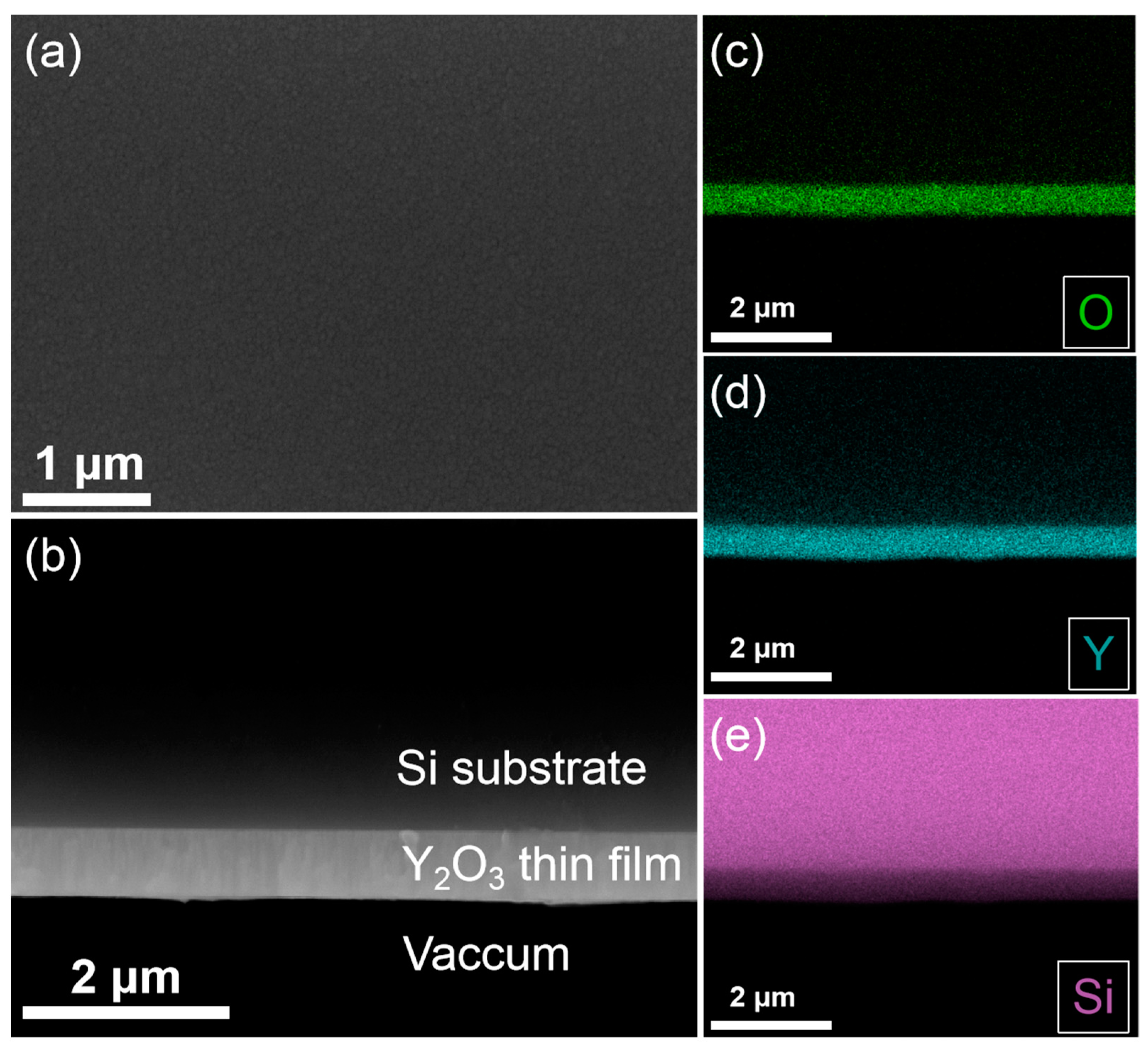
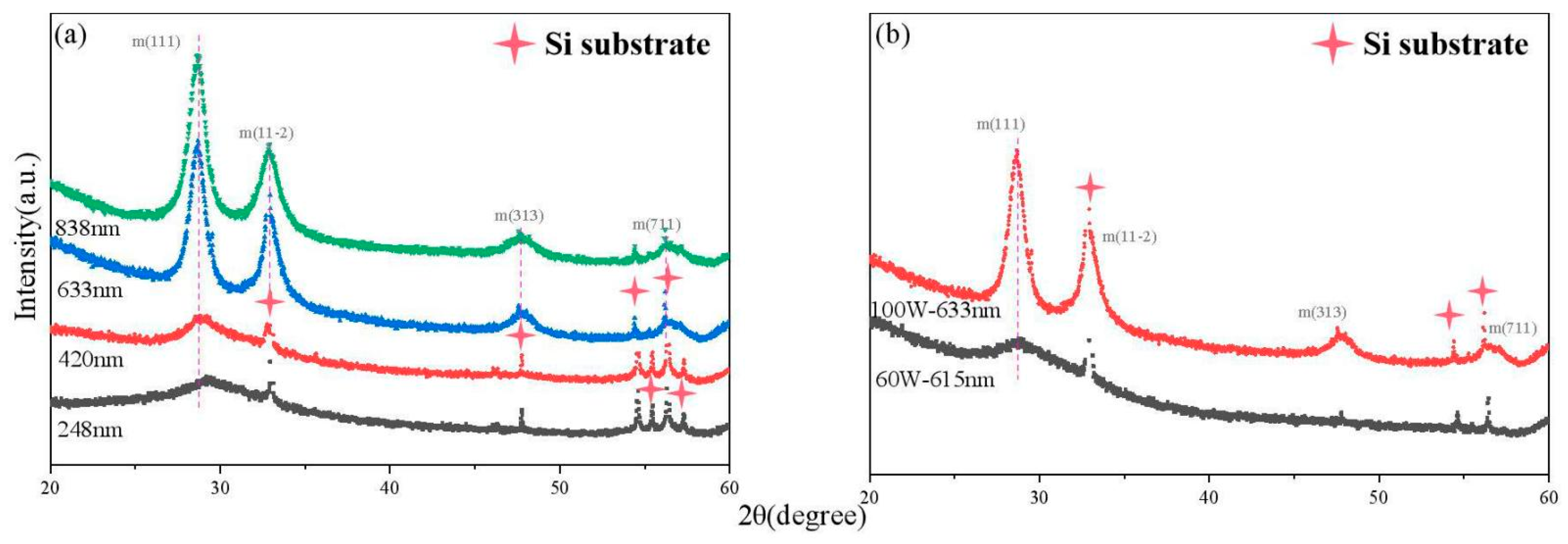
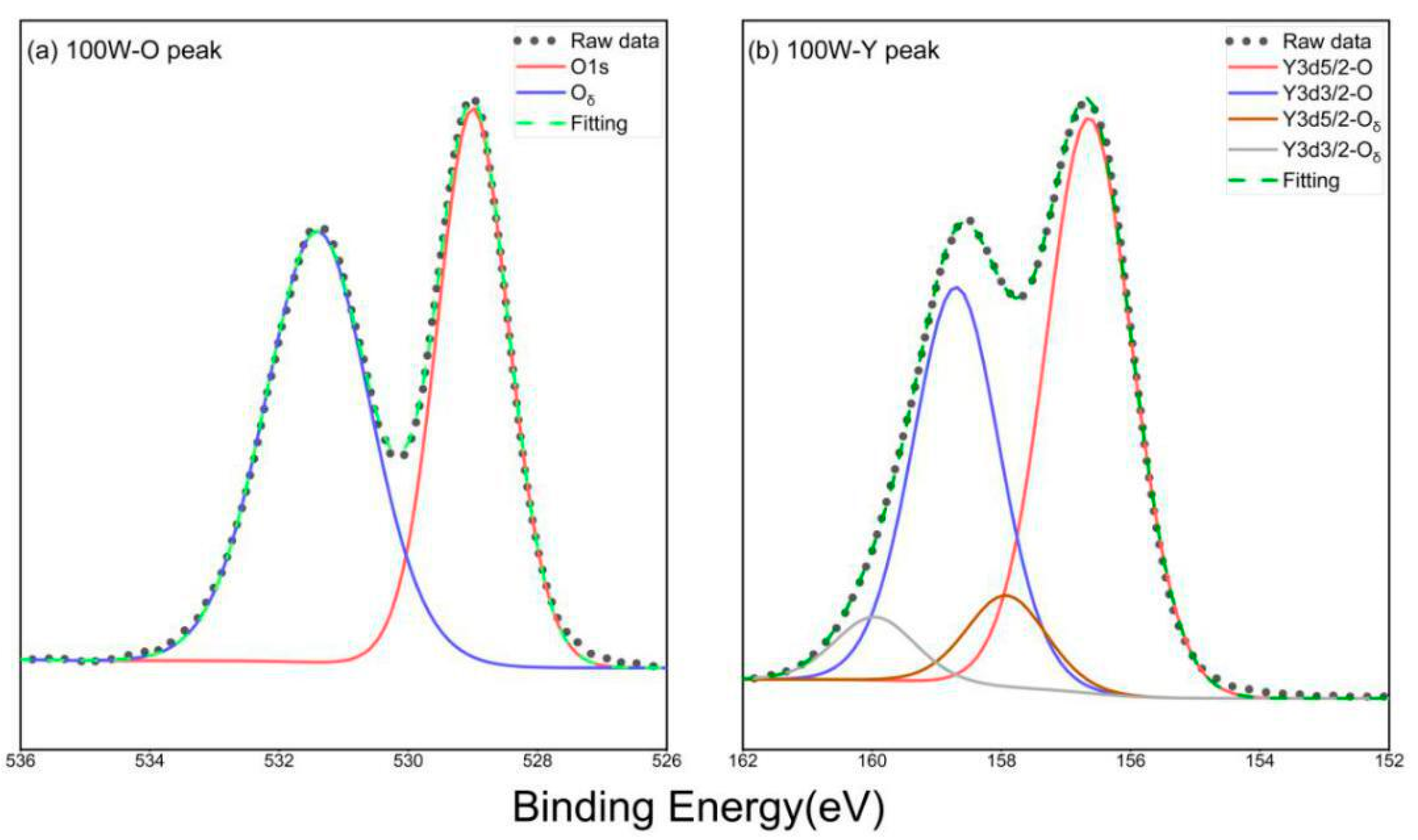
3.1. The Crystalline Structure and Chemical Bonding of the Y2O3 Films

The crystalline structure and orientations of the Y2O3 films were investigated by XRD, as shown in Figure 2. When the sputtering power is 100 W, the crystallinity of the Y2O3 film changes obviously with the increase in thickness. The as-deposited thin films show an amorphous character at the thicknesses of 248 nm and 420 nm, respectively. There is only a broad and flat peak at 25–33°, as shown in Figure 2a. As the thickness increases to 633 nm and above, the films are crystallized and have a monoclinic structure. The highest peak at 28.7° is m (111), and the other peaks, including m (11 2 ¯ ), (313) and (711) coexist, although they are very weak. For thicker films, a prolonged dense bombardment of sputtered atoms/clusters/ions can lead to an increased substrate temperature and film crystallinity with a longer deposition time [28]. However, when the deposition power is decreased to 60 W, all of the films are amorphous. This is probably due to the very slow sputtering rate in poison mode. Regarding the deposition of Y2O3 thin films at room temperature, different structures including amorphous, monoclinic, and cubic phases have been observed previously [2,9,29]. It has been revealed that factors including reduced oxygen partial pressure [3], increased substrate bias [9], and sputtering power [30] can lead to the formation of monoclinic phases. However, the films usually transfer to a stable cubic phase after post-annealing [23,24], as discussed below.
Figure 3 shows the XPS spectra of O1s and Y3d. It can be seen that two sub-peaks exist for O1s, which are located near 529 eV and 531.41 eV, corresponding to the O-Y bond and Oδ (physically absorbed oxygen) [23], respectively. Oδ exists inevitably in Y2O3 films prepared by reactive magnetron sputtering at room temperature [19,23,31], although the samples were pre-sputtered using Ar. For yttrium, the Y 3d core is split into two pairs of peaks. The first pair is the Y-O bond of Y3d5/2 and Y3d3/2, located around 156.65 eV and 158.7 eV, respectively; the second pair is the Y-Oδ bond of Y3d5/2 and Y3d3/2 at 157.92 eV and 159.96 eV, respectively [1]. A metal Y3d peak is not observed at 155.6 eV, indicating that no metal yttrium exists in the film [22].

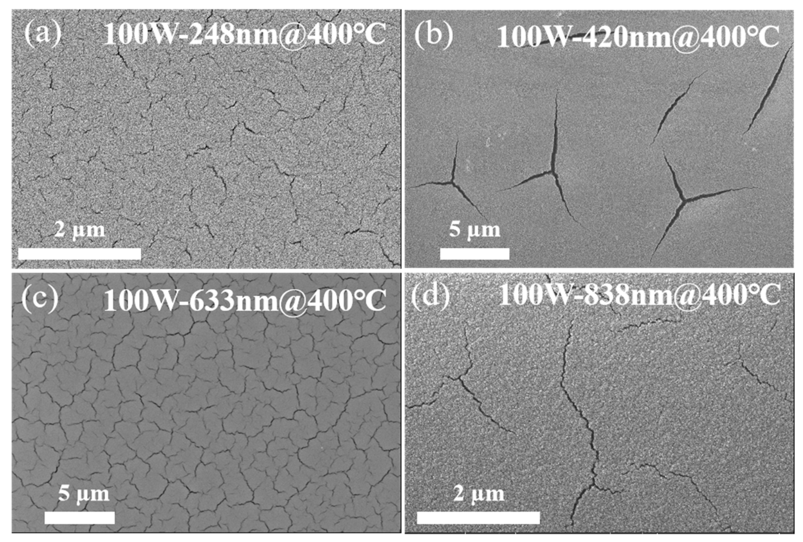
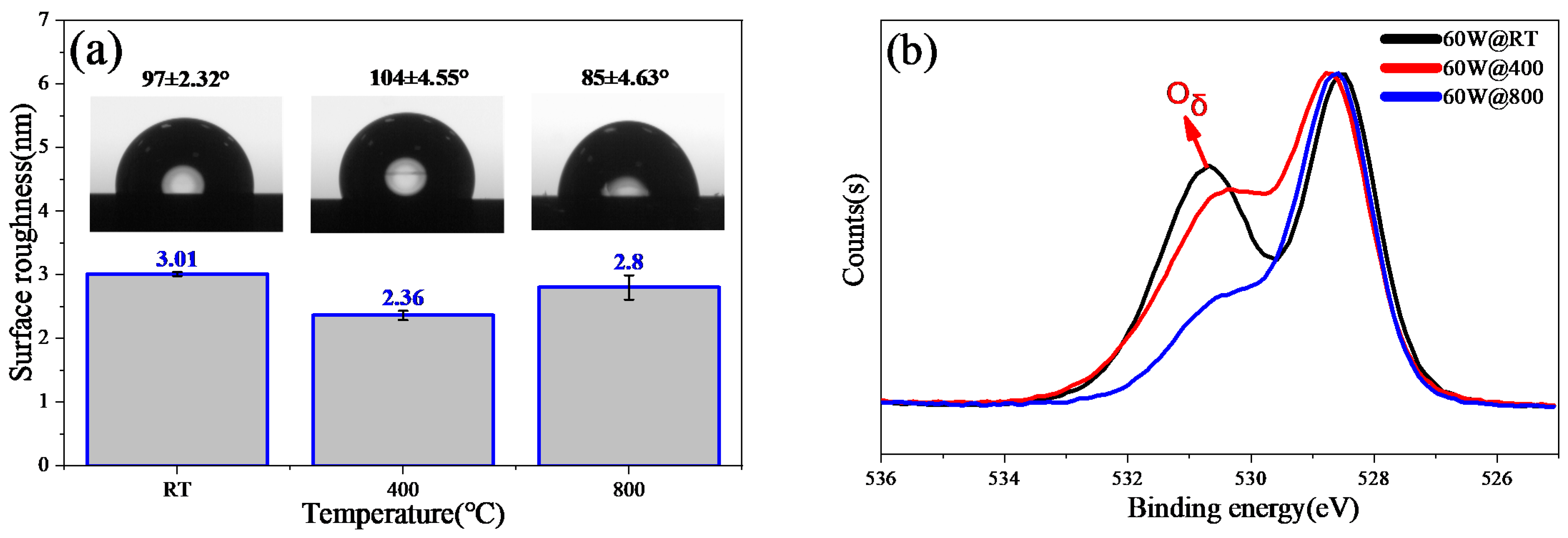
3.2. Post-Annealing Treatment of the Film

We further annealed the samples in static air at 400 °C for 2 h and examined the microstructure evolution of the thin films. After annealing at 400 °C, two sets of films transformed to the most stable cubic phase with c(222) as the preferred orientation, as shown in Figure 4. For the 100 W Y2O3 samples, various degrees of cracks appeared on the surfaces, as shown in Figure 5. This is probably due to the large difference in the thermal expansion coefficient between the substrate (2.6 × 10⁻⁶/K) and Y2O3 (8.1 × 10⁻⁶/K) [18]. However, in poison deposition mode with a deposition power of 60 W, no crack was observed for samples with a thickness in the range of 220 to 1015 nm in the present study after being annealed at 400 °C in Figure 6. Similar phenomena have been observed for a reactive sputtered Y2O3 thin film on P92 steel [18], in which the thin film with a cubic phase cracked but the one with a monoclinic structure maintained thin-film integrity after annealing at 600 °C. This has been attributed to the formation of a porous monoclinic structure, which allows for stress relaxation during heat treatment. However, the films with a monoclinic phase deposited at 100 W in the present study cracked after heat treatment. A careful comparison of the experimental details suggests that the uncracked thin films in the present study and the literature [18] were all prepared in poison mode with a relatively high O2 flow rate or low sputtering power, while the cracked ones were sputtered in metallic mode with no regard for what crystalline structures the films had. This is consistent with the result in ref [24], in which the Y2O3 film sputtered from a Y2O3 compound target could sustain up to 900 °C without cracking. In reactive sputtering, sputtering from a Y2O3 compound target or a poisoned target (a thin Y2O3 capping layer formed on the Y surface) typically results in a much slower deposition rate than that for a metallic Y target. In addition, it has been found that the amounts of high-energy-negative ions (O) produced in poison mode are several orders of magnitude higher than those in metallic mode [32], which can result in more defects in the as-deposited films. The highly disordered structure must play a significant role in allowing stress redistribution [33,34] during heat treatment-induced recrystallization and the inhibition of crack formation.

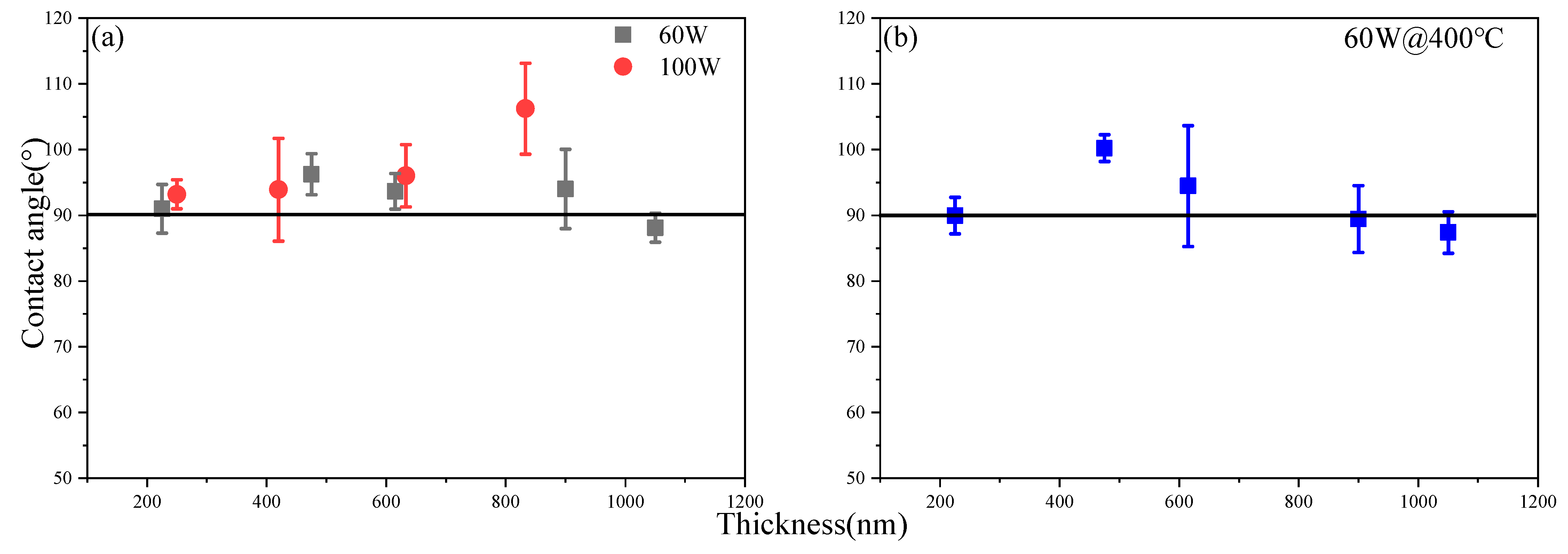
3.3. The Wetting Properties of the Y2O3 Film

Figure 7 illustrates the wetting properties of the Y2O3 thin films; all of the as-deposited films at the two sputtering powers are hydrophobic, with water contact angles above 90°, except for the 60 W sample with a thickness of 1015 nm (88.12 ± 2.20°). The water contact angle of samples deposited at 100 W increases with the thickness, and its maximum is 106.23 ± 6.93°, while there is no significant difference for 60 W samples of different thicknesses. After annealing at 400 °C, only the 60 W samples were measured, as all of the 100 W samples cracked. In general, the water contact angles remained ≥90°, indicating robust hydrophobicity.
In order to understand the post-annealing effect on the evolution of Y2O3 thin-film wetting properties, we further heat-treated sample 2-2 (60 W, 475 nm) at a higher temperature of 800 °C. The film was very robust, without cracks even when annealed at 800 °C for 2 h. As shown in Figure 8a, the water contact angle increased to 104 ± 4.55° at 400 °C but decreased to 85 ± 4.63°. Because the wettability property of a solid surface can be affected by the surface morphology and chemical composition of the thin films, we further compared the evolution of the surface roughness and surface chemistry of sample 2-2 before and after heat treatment, as shown in Figure 8a. The surface roughness remains ~3 nm, even though the thin film becomes crystalline after annealing. However, the XPS spectra are quite different. The intensity of the low binding energy component of O1s remains unchanged, which represents the Y-O bond; however, the intensity of the Oδ component as indicated by the red arrow in Figure 8b, which decreases and moves towards a lower binding energy after heat treatment, suggesting the desorption of the Oδ from the thin film. It is well known that the oxygen concentration has a significant effect on the wettability of yttrium oxide [10,13,35]. The initial O/Y in the film is as high as 2.05. The high oxygen content can increase the electron density of yttrium cores, and leads to a repulsive interaction between the yttrium metals and the oxygen in the water [10]. Previous results found that the desorption of Oδ occurs at a temperature of 260 °C for Y2O3 powders [23]. However, the desorption of Oδ in a Y2O3 thin film is more complex and slower, which is a surface-related process and can be affected by several factors, including the initial oxygen content, annealing temperature, and film thickness, etc. At 400 °C, the phase transformation (amorphous to cubic) and the columnar structure limit the channel of oxygen desorption. As shown in Figure 8b, the Oδ sub-peak of the Y2O3 thin film after heat treatment at 400 °C is just slightly lower than that of the as-deposited one. During desorption, the internal species continue diffusing from inside to the surface, resulting in a high oxygen concentration on the film surface. Therefore, the hydrophobicity of Y2O3 is sustained after annealing at 400 °C. However, at 800 °C, the much faster desorption of Oδ—as indicated by the small Oδ sub-peak in Figure 8b—leads to a reduction of the water contact angle on the Y2O3 surface.

4. Conclusions

In summary, Y2O3 films were fabricated on an Si wafer by reactive DC magnetron sputtering, and the effects of heat treatment on the Y2O3 thin-film microstructure and wettability properties were studied. Two sets of samples with different thicknesses were prepared in metallic mode and poison mode by varying the deposition power. The films deposited in metallic mode have amorphous or monoclinic structures, and all of the samples with different thicknesses become cracked after annealing at 400 °C in air. However, the thin films deposited in poison mode are amorphous, and transform to the most stable cubic phase after heat treatment. All of the films have water contact angles above 90° in an as-deposited state. Moreover, the Y2O3 thin films prepared in poison mode remained hydrophobic even after being exposed to high temperatures. Further XPS analysis results suggests that the physically absorbed oxygen in the poisoned mode has an important effect on the film hydrophobicity. All of these results can provide guides for industry engineering and the optimization of hydrophobic Y2O3 protective coatings.

Author Contributions

X.M. carried out the sample deposition process and the characterizations, including the SEM, XRD and wettability testing; Z.H. provided the AFM and XPS results, and measured the film thickness. L.F. analyzed the results, revised the manuscript and directed the work. All authors have read and agreed to the published version of the manuscript.

Funding

This research was funded by the National Natural Science Foundation of China (Grant No. 51902351); the Natural Science Foundation of Guangdong Province, China (Grant No. 2019A1515010693); and the Open Fund of Guangdong Provincial Key Laboratory of Luminescence from Molecular Aggregate, Guangzhou 510640, China (South China University of Technology) (Grant No. 2019-kllma-10).

Institutional Review Board Statement

Not applicable.

Informed Consent Statement

Not applicable.

Data Availability Statement

Not applicable.

Conflicts of Interest

The authors declare no conflict of interest. The funders had no role in the design of the study; in the collection, analyses, or interpretation of data; in the writing of the manuscript, or in the decision to publish the results.

References

  1. Yu, P.; Zhang, K.; Huang, H.; Wen, M.; Li, Q.; Zhang, W.; Hu, C.; Zheng, W. Oxygen vacancies dependent phase transition of Y2O3 films. Appl. Surf. Sci. 2017, 410, 470–478. [Google Scholar] [CrossRef]
  2. Hua, C.; Li, C.; Guo, J.; Yan, X.; Liu, J.; Chen, L.; Wei, J.; Hei, L. Optical properties of cubic and monoclinic Y2O3 films prepared through radio frequency magnetron sputtering. Surf. Coat. Technol. 2017, 320, 279–283. [Google Scholar] [CrossRef]
  3. Hua, C.; Chen, L.; Li, C.; Wang, M.; Guo, J.; Liu, J.; Yan, X.; Zhao, Y.; An, K.; Wei, J.; et al. Effects of oxygen-to-argon ratio on crystalline structure and properties of Y2O3 anti-reflection films for freestanding CVD diamond. J. Alloy. Compd. 2017, 693, 468–473. [Google Scholar] [CrossRef]
  4. Jeong, J.Y.; Kim, J.H. Structure and Photoluminescence of Optically Transparent Y2O3:Eu Thin Films Prepared on Sapphire Substrates by RF Magnetron Sputtering. Appl. Sci. Converg. Technol. 2021, 30, 34–37. [Google Scholar] [CrossRef]
  5. Lei, P.; Chen, X.; Yan, Y.; Zhu, J. The tunable dielectric properties of sputtered yttrium oxide films. Appl. Phys. A 2021, 127, 99. [Google Scholar] [CrossRef]
  6. Lizarraga-Medina, E.G.; Caballero-Espitia, D.L.; Jurado-Gonzalez, J.; López, J.; Marquez, H.; Contreras-López, O.E.; Tiznado, H. Al2O3-Y2O3 nanolaminated slab optical waveguides by atomic layer deposition. Opt. Mater. 2020, 103, 109822. [Google Scholar] [CrossRef]
  7. Quah, H.J.; Cheong, K.Y. Effects of post-deposition annealing ambient on Y2O3 gate deposited on silicon by RF magnetron sputtering. J. Alloy. Compd. 2012, 529, 73–83. [Google Scholar] [CrossRef]
  8. Chopade, S.S.; Barve, S.A.; Thulasi Raman, K.H.; Chand, N.; Deo, M.N.; Biswas, A.; Rai, S.; Lodha, G.S.; Rao, G.M.; Patil, D.S. RF plasma MOCVD of Y2O3 thin films: Effect of RF self-bias on the substrates during deposition. Appl. Surf. Sci. 2013, 285, 524–531. [Google Scholar] [CrossRef] [Green Version]
  9. Lei, P.; Dai, B.; Zhu, J.; Chen, X.; Liu, G.; Zhu, Y.; Han, J. Controllable phase formation and physical properties of yttrium oxide films governed by substrate heating and bias voltage. Ceram. Int. 2015, 41, 8921–8930. [Google Scholar] [CrossRef]
  10. Gischkat, T.; Döbeli, M.; Bächli, A.; Botha, R.; Balogh-Michels, Z. Influence of Ar-impurities on the wettability of IBS-deposited Y2O3 thin films. Appl. Surf. Sci. 2021, 568, 150880. [Google Scholar] [CrossRef]
  11. Zhao, B.; Mattelaer, F.; Rampelberg, G.; Dendooven, J.; Detavernier, C. Thermal and Plasma-Enhanced Atomic Layer Deposition of Yttrium Oxide Films and the Properties of Water Wettability. ACS Appl. Mater. Interfaces 2020, 12, 3179–3187. [Google Scholar] [CrossRef] [PubMed]
  12. Oh, I.-K.; Kim, K.; Lee, Z.; Ko, K.Y.; Lee, C.-W.; Lee, S.J.; Myung, J.M.; Lansalot-Matras, C.; Noh, W.; Dussarrat, C.; et al. Hydrophobicity of Rare Earth Oxides Grown by Atomic Layer Deposition. Chem. Mater. 2015, 27, 148–156. [Google Scholar] [CrossRef]
  13. Azimi, G.; Dhiman, R.; Kwon, H.-M.; Paxson, A.T.; Varanasi, K.K. Hydrophobicity of rare-earth oxide ceramics. Nat. Mater. 2013, 12, 315–320. [Google Scholar] [CrossRef] [PubMed]
  14. Barshilia, H.C.; Chaudhary, A.; Kumar, P.; Manikandanath, N.T. Wettability of Y2O3: A Relative Analysis of Thermally Oxidized, Reactively Sputtered and Template Assisted Nanostructured Coatings. Nanomaterials 2012, 2, 65. [Google Scholar] [CrossRef] [Green Version]
  15. Ahmad, D.; van den Boogaert, I.; Miller, J.; Presswell, R.; Jouhara, H. Hydrophilic and hydrophobic materials and their applications. Energy Sources Part A Recovery Util. Environ. Eff. 2018, 40, 2686–2725. [Google Scholar] [CrossRef]
  16. Feng, Y.; Huang, Y.; Liu, J.; Chen, L.; Wei, J.; Li, C. Research Progress of Rare Earth Infrared Anti-reflection Films. Chin. J. Rare Met. 2019, 43, 1346–1356. [Google Scholar]
  17. Ellmer, K.; Welzel, T. Reactive magnetron sputtering of transparent conductive oxide thin films: Role of energetic particle (ion) bombardment. J. Mater. Res. 2012, 27, 765–779. [Google Scholar] [CrossRef]
  18. Mao, Y.; Engels, J.; Houben, A.; Rasinski, M.; Steffens, J.; Terra, A.; Linsmeier, C.; Coenen, J.W. The influence of annealing on yttrium oxide thin film deposited by reactive magnetron sputtering: Process and microstructure. Nucl. Mater. Energy 2017, 10, 1–8. [Google Scholar] [CrossRef]
  19. Lei, P.; Zhu, J.; Zhu, Y.; Jiang, C.; Yin, X. Yttrium oxide thin films prepared under different oxygen-content atmospheres: Microstructure and optical properties. Appl. Phys. A 2012, 108, 621–628. [Google Scholar] [CrossRef]
  20. Endoh, R.; Nakamura, K.; Fujita, H.; Matsunaga, M.; Kimura, K.; Riesch, J.; Hishinuma, Y.; Chikada, T. Deuterium permeation behavior through yttria-stabilized zirconia coating fabricated by magnetron sputtering. Fusion Eng. Des. 2020, 157, 111769. [Google Scholar] [CrossRef]
  21. Xia, J.; Liang, W.; Miao, Q.; Depla, D. On the influence of local oxygen addition on the growth of sputter deposited yttrium oxide thin films. Surf. Coat. Technol. 2019, 357, 768–773. [Google Scholar] [CrossRef]
  22. Lei, P.; Zhu, J.; Zhu, Y.; Jiang, C.; Yin, X. Evolution of composition, microstructure and optical properties of yttrium oxide thin films with substrate temperature. Surf. Coat. Technol. 2013, 229, 226–230. [Google Scholar] [CrossRef]
  23. Xu, S.; Yao, Z.; Zhou, J.; Du, M. Effects of post-deposition annealing on the chemical composition, microstructure, optical and mechanical properties of Y2O3 film. Surf. Coat. Technol. 2018, 344, 636–643. [Google Scholar] [CrossRef]
  24. Abubakar, S.; Kaya, S.; Aktag, A.; Yilmaz, E. Yttrium oxide nanostructured thin films deposited by radio frequency sputtering: The annealing optimizations and correlations between structural, morphological, optical and electrical properties. J. Mater. Sci. Mater. Electron. 2017, 28, 13920–13927. [Google Scholar] [CrossRef]
  25. Yan, F.; Liu, Z.T.; Liu, W.T. The properties of the Y2O3 films exposed at elevated temperature. Phys. B Condens. Matter 2011, 406, 2827–2833. [Google Scholar] [CrossRef]
  26. Yu, Z.; Liang, L.Y.; Liu, Z.M.; Xu, W.Y.; Sun, X.L.; Cao, H.T. Effects of sputtering pressure and post-metallization annealing on the physical properties of rf-sputtered Y2O3 films. J. Alloy. Compd. 2011, 509, 5810–5815. [Google Scholar] [CrossRef]
  27. Lei, P.; Leroy, W.; Dai, B.; Zhu, J.; Chen, X.; Han, J.; Depla, D. Study on reactive sputtering of yttrium oxide: Process and thin film properties. Surf. Coat. Technol. 2015, 276, 39–46. [Google Scholar] [CrossRef]
  28. Zhao, C.; Zhao, L.; Liu, J.; Liu, Z.; Chen, Y. Effect of sputtering power on the properties of SiO2 films grown by radio frequency magnetron sputtering at room temperature. Opt. Quantum Electron. 2021, 53, 15. [Google Scholar] [CrossRef]
  29. Mudavakkat, V.H.; Atuchin, V.V.; Kruchinin, V.N.; Kayani, A.; Ramana, C.V. Structure, morphology and optical properties of nanocrystalline yttrium oxide (Y2O3) thin films. Opt. Mater. 2012, 34, 893–900. [Google Scholar] [CrossRef]
  30. Yan, F.; Liu, Z.T.; Liu, W.T. Structural and optical properties of yttrium trioxide thin films prepared by RF magnetron sputtering. Vacuum 2011, 86, 72–77. [Google Scholar] [CrossRef]
  31. Cho, M.H.; Ko, D.H.; Jeong, K.; Whangbo, S.W.; Whang, C.N.; Choi, S.C.; Cho, S.J. Structural transition of crystalline Y2O3 film on Si(111) with substrate temperature. Thin Solid Film. 1999, 349, 266–269. [Google Scholar] [CrossRef]
  32. Mahieu, S.; Leroy, W.P.; Van Aeken, K.; Depla, D. Modeling the flux of high energy negative ions during reactive magnetron sputtering. J. Appl. Phys. 2009, 106, 093302. [Google Scholar] [CrossRef]
  33. Gaboriaud, R.J.; Pailloux, F.; Perriere, J. Pulsed laser deposition of Y2O3 thin films on MgO. Appl. Surf. Sci. 2002, 186, 477–482. [Google Scholar] [CrossRef]
  34. Gaboriaud, R.J.; Pailloux, F.; Paumier, F. Characterisation of Y2O3 thin films deposited by laser ablation on MgO: Why a biaxial epitaxy. Appl. Surf. Sci. 2002, 188, 29–35. [Google Scholar] [CrossRef]
  35. Gąszowski, D.; Ilczyszyn, M. Hydrogen bonding to xenon: A comparison with neon, argon and krypton complexes. Chem. Phys. Lett. 2013, 556, 59–64. [Google Scholar] [CrossRef]
Figure 1. (a,b) are SEM images from the top and cross-section of the as-deposited Y2O3 film (sample 1-3); (ce) are the distribution of the O, Y, and Si elements from the EDS mapping results.
Coatings 12 00790 g001
Figure 2. (a) The evolution of the as-deposited Y2O3 films’ XRD patterns (samples 1-1 to 1-4); (b) comparison of the XRD patterns of samples 1-3 and 2-3.
Coatings 12 00790 g002
Figure 3. The XPS spectra of (a) the O1s core level and (b) the Y3d core level of the as-deposited Y2O3 thin film (samples 1–3).
Coatings 12 00790 g003
Figure 4. The XRD patterns of Y2O3 films (samples 1-3 and 2-3) annealed at 400 °C.
Coatings 12 00790 g004
Figure 5. (ad) are the SEM images of Y2O3 films (samples 1-1 to 1-4) annealed at 400 °C.
Coatings 12 00790 g005
Figure 6. (ae) are the SEM images of Y2O3 films (samples 2-1 to 2-5) annealed at 400 °C.
Coatings 12 00790 g006
Figure 7. The water contact angles of Y2O3 films for (a) as-deposited samples 1-1 to 1-4 and 2-1 to 2-5, and (b) samples 2-1 to 2-5 after annealing at 400 °C.
Coatings 12 00790 g007
Figure 8. (a) The surface roughness and the water contact angles, (b) the XPS spectra of the oxygen of the Y2O3 film (sample 2-2) annealed at different temperatures.
Coatings 12 00790 g008
Table 1. The information of the as-deposited Y2O3 thin films.
SampleDeposition Power (W)Thickness (nm)
1-1100248
1-2100420
1-3100633
1-4100838
1-51001010
2-160225
2-260476
2-360615
2-460900
2-5601015
Publisher’s Note: MDPI stays neutral with regard to jurisdictional claims in published maps and institutional affiliations.

