Article

Electro-Assisted 3D Printing Multi-Layer PVDF/CaCl2 Composite Films and Sensors

1
School of Materials Science and Engineering, Jiangsu University, Zhenjiang 212013, China
2
School of Mechanical & Intelligent Manufacturing, Jiujiang University, Jiujiang 332005, China
*
Author to whom correspondence should be addressed.
Coatings 2022, 12(6), 820; https://doi.org/10.3390/coatings12060820
Submission received: 8 May 2022 / Revised: 8 June 2022 / Accepted: 9 June 2022 / Published: 11 June 2022

Abstract

:
Polyvinylidene fluoride (PVDF) films are widely used in sensors for their wide response frequency, good flexibility, low acoustic impedance, and chemical stability. In this work, PVDF/CaCl2 piezoelectric films were prepared by an electro-assisted 3D printing method and used to form a multi-layer composite film sensor. The study found that the addition of CaCl2 can effectively increase the β-phase content in the PVDF film and improve the piezoelectric and dielectric properties of the PVDF composite film sensors. When the content of CaCl2 is 0.15 wt.%, the β-phase content of the PVDF/CaCl2 composite film can reach the highest value of up to 48.47%, and the output voltage response of the sensor is 0.62 V at an input frequency of 10 Hz, 10 V voltage. The output voltage of PVDF composite film sensor with two and three layers is 1.306 and 1.693 times that of a single layer, respectively. The sensitivity of the multi-layer sensors has also been greatly improved.

1. Introduction

Polyvinylidene fluoride (PVDF) flexible film sensors have the ability to feel mechanical deformation or vibration through the piezoelectric effect and turn them into electrical signals. It is widely used to measure the physical quantities of dynamic force, acceleration, vibration displacement, and structural strain in engineering and some other areas [1,2].
Compared with the traditional piezoelectric ceramic sensors, polymer-based PVDF film sensors inherently show a weaker sensing signal, which is due to the poor piezoelectric performance of PVDF film. However, its characteristics of high flexibility, wide frequency response, and strong impact resistance are still useful for researchers. PVDF polymers usually have a non-polar α-phase under normal crystallization conditions. In order to change the dipole distribution of PVDF polymer and generate the piezoelectric effect in the crystal structure, an electric polarization measure is often applied to promote the formation of β-phase with the strongest electrical activity. For example, Chen et al. reported that the PVDF molecular chains were stretched to form an orderly arrangement by the pulling of in situ strong electric potential, which improved the formation of the β-phase and polarize the PVDF film simultaneously [3]. On this basis, more researchers have begun to prepare nanocomposites (PVDF/BaTiO3) or add additives (CNT, Cu) to further increase the β-phase content of the PVDF films, so as to improve their piezoelectric and dielectric properties [4,5]. In this regard, Sobhan added 0.8 wt.% BaTiO3 nanoparticles to the PVDF polymer, and it was observed that the content of the β-phase increased, thereby improving the output voltage response of the sensor [6]. In 2020, Ramadoss further discovered that when 12 wt.% BaTiO3 was doped, the electrospun PVDF/BaTiO3 composite material had a maximum β-phase ratio of 75% [7].
On the basis of single-layer film sensors, multi-layer sensors have also been developed. Karanth studied sensors with multi-layer PVDF piezoelectric film structure through finite element simulation, and the results showed that the performance of multi-layer PVDF sensors was improved [8]. Lee and others prepared a multi-layer PVDF piezoelectric film sound pressure energy harvester and found that four-layer PVDF piezoelectric film can improve the energy harvesting efficiency [9]. In 2014, Zhao embedded multi-layer PVDF piezoelectric film in shoes, and energy harvested from walking [10]. In 2016, Spanu developed a low-voltage floating-gate organic transistor coupled to a PVDF capacitor on the sensing area, making it an excellent high-sensitivity tactile sensor. By changing the second gate geometry, the applied pressure of the device reached a lower sensitivity limit of 300 Pa [11].
In order to further improve the performance of the PVDF film sensors, PVDF/CaCl2 composite films were prepared by electro-assisted 3D printing. The effect of CaCl2 on the crystal structure and properties of the PVDF/CaCl2 composite film were studied. The sensitivity of the multi-layer PVDF/CaCl2 film sensor was also explored.

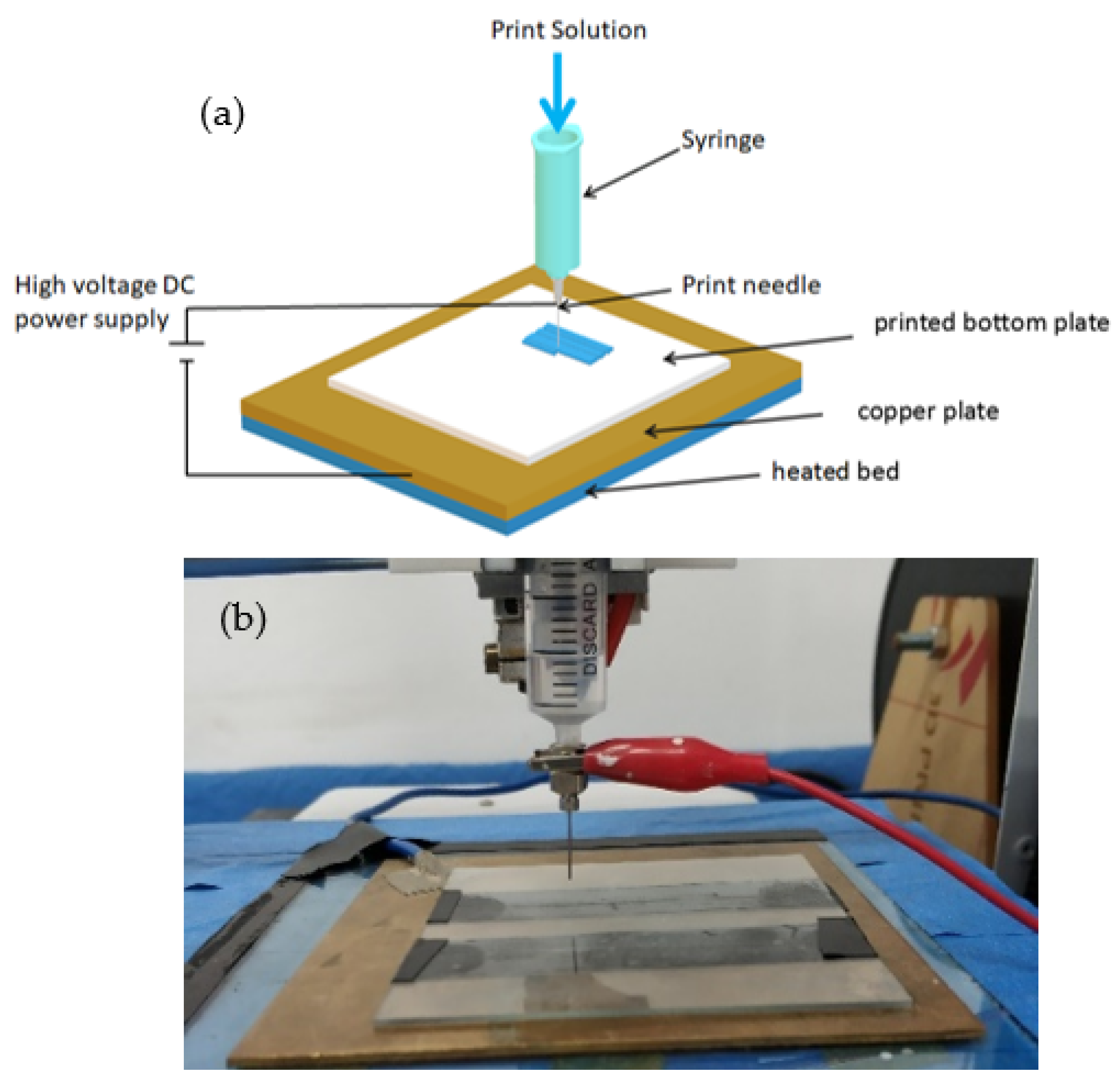
2. Materials and Methods

CaCl2 powder (Analytical Pure, Sinopharm Group, Shanghai, China) with a content of 0–0.30 wt.% was added into N-Methyl pyrrolidone solvent (NMP, 96%, Shanghai Aladdin, Shanghai, China), ultrasonically treated for 3 h, and the CaCl2 powder was uniformly dispersed in the solvent, then 16 wt.% PVDF powder (molecular weight 30 w, French Arkema, Shanghai, China) was dissolved in the solvent until complete dissolution after sonicating for 2 h. Then the print solution was obtained when the 0.1 wt.% acetone (C3H6O, 96%, Sinopharm Group, Shanghai, China) was added to the mixed solution and ultrasonized for 1 h.
An improved 3D printer with high DC voltage was used to print PVDF/CaCl2 composite films, as shown in Figure 1. The printer parameters were set as follows: the distance between the printing needle and the glass printed bottom plate was 2 mm, 6 kV high voltage was applied between the needle tip, and the copper plate and the temperature of the heated bed was 80 °C. After printing 70 layers one by one, a flexible composite film with a size of 20 mm × 20 mm and a thickness of about 45 μm was prepared.
After depositing a layer of 20 μm gold films on the upper and lower surfaces of the PVDF/CaCl2 composite film as electrodes with a vacuum ion sprayer (MC1000, Hitachi, Kyoto, Japan), a single-layer sensor is formed. A double-layer sensor was obtained by repeatedly printing PVDF/CaCl2 composite films of the same thickness on the upper surface of the gold electrode and then depositing another gold film on the surface of the printed film. By repeatedly printing the PVDF/CaCl2 composite films and depositing the gold electrode film on them, a three-layer sensor was obtained. The double-layer and three-layer sensors were composed of two or three layers of film stacked in series respectively.
A Fourier infrared spectrometer (Nicolet 6700, Waltham, Thermo Fisher Scientific, MA, USA) was used to determine the functional groups and crystal forms contained in the PVDF composite piezoelectric film. Equation (1) can be used to calculate the relative content of the β-phase in the film, combined with the FTIR spectrum.
F(β) = A(β)/(1.26A(α) + A(β))
where A(α)and A(β) represent the absorption peaks at 763 cm−1 and 840 cm−1 in the FTIR graph respectively [12]. An X-ray diffractometer (D/max2500 PC, Rigaku Co., Tokyo, Japan) was used to determine the crystallinity of the film sample. The β-phase content in the film is obtained by the product of the crystallinity and F(β).
Used the LCR digital bridge (TH2816A, Changzhou Tonghui Electronics Co., LTD, Changzhou, China) we detected the capacitance value at each frequency, and calculated the relative permittivity of PVDF/CaCl2 composite film by Equation (2).
εr = (C × d)/(ε0 × S)
where εr is the relative permittivity, C is the PVDF/CaCl2 composite film capacitor, d is the thickness of the PVDF/CaCl2 composite film, ε0 is the vacuum permittivity (8.854 × 10⁻¹² F/m), and S is the area of the PVDF/CaCl2 composite film electrode [13].
The performance of both single-layer and multi-layer sensors was tested by a cantilever beam structure, as shown in Figure 2. The PVDF/CaCl2 composite film sensor attached to a sheet of manganese steel was 7 cm away from the root of the cantilever. The PZT actuator was 15 cm away from the root of the cantilever, which was used as a driver to drive the vibration of the cantilever. The output voltage signal of the PVDF/CaCl2 composite film sensor was passed through a low-pass filter, a signal amplifier, and an oscilloscope in turn to collect the electrical signal.

3. Results

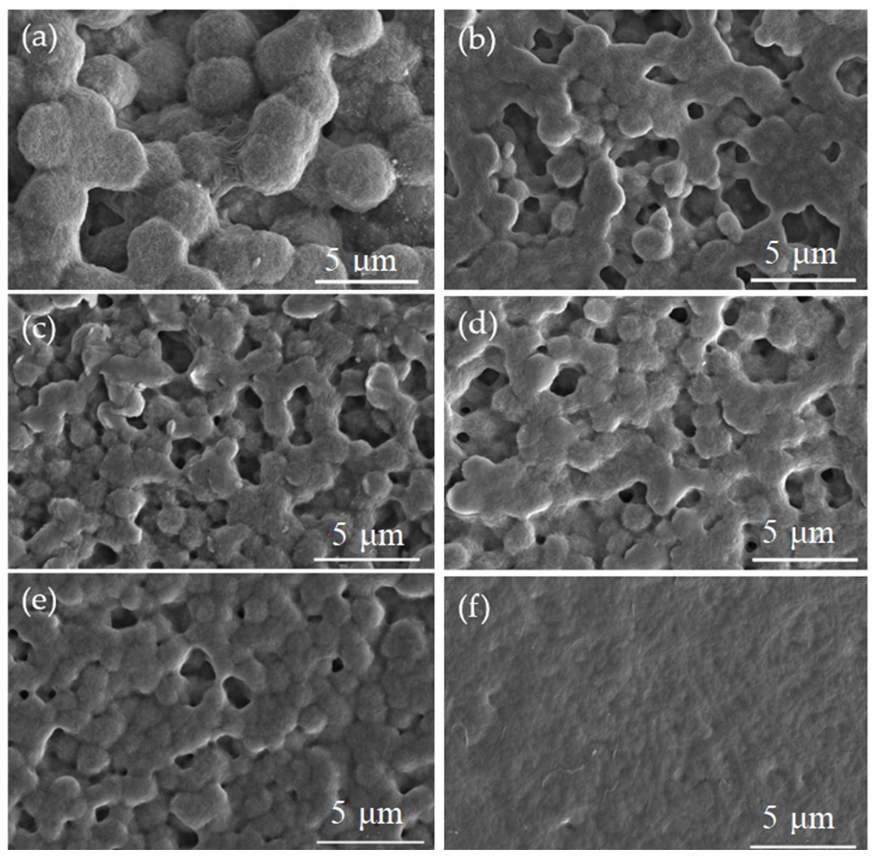
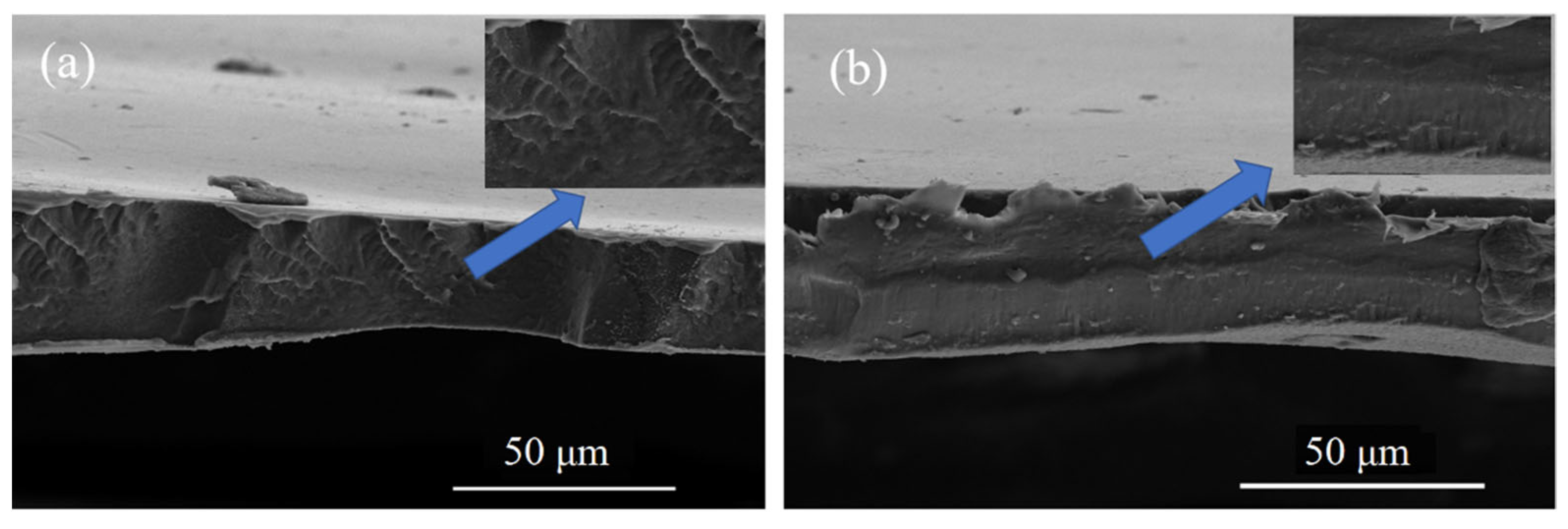
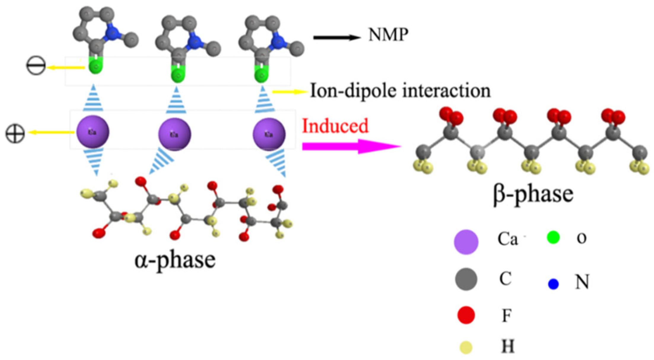
3.1. Microstructure Analysis of PVDF/CaCl2 Composite Film

Figure 3 is the SEM surface topography of pure PVDF film and PVDF/CaCl2 composite film. It can be seen from the figure that these films are composed of numerous spherulites with pores between them. The average spherulite size of pure PVDF film is about 3.5 μm, as shown in Figure 3a. When the film contained 0.05 wt.% CaCl2, the spherulite size became smaller and PVDF film had larger pores, as shown in Figure 3b. With the further increase of CaCl2 content, the pores continue to decrease and the size of spherulites is about 1.5 μm, as shown in Figure 3c–e. When CaCl2 content increases to 0.3 wt.%, spherulites are smaller and the surface of the film presents a compact state without pores, as shown in Figure 3f. Figure 4 is the transverse topography of the PVDF film. It can be observed from the two figures that there are obvious pores in the transverse direction of the pure PVDF film, while the pores in the transverse direction of composite film with 0.3 wt.% CaCl2 are greatly reduced, the magnified images are shown in the upper right corner of Figure 4a,b. It indicates that the quality of the film is improved with the addition of the appropriate amount of CaCl2.
Figure 5a shows the XRD patterns of pure PVDF film and PVDF composite films with different CaCl2 contents. It can be seen from the Figure 5a that the pure PVDF film has obvious double characteristic absorption peaks, 2θ = 18.4° corresponds to the (020) crystal plane of α-phase, and 20.6° corresponds to the (020) crystal plane of β-phase, which indicates that both of the α- and β-phase are simultaneously present in the pure PVDF film. However, comparing the diffraction peaks of the PVDF/CaCl2 composite film and the pure PVDF film, the characteristic peaks on the (110) crystal plane with CaCl2 added are sharper, which indicates that the addition of CaCl2 increases the crystallinity of the β-phase [14,15,16]. Figure 4b shows the FTIR spectra of PVDF film, we can also see the characteristic bands of 763 cm−1, 975 cm−1, 1150 cm−1, 1209 cm−1, and 1384 cm−1 representing α-phase [17,18] and the characteristic bands of β-phase appear at 840 cm−1 and 1274 cm−1 [19,20], while γ-phase appears at 1400 cm−1, indicates that the α-, β-, and γ-phases coexist in PVDF films [21,22]. Combined with the XRD spectra, the main crystalline phases of PVDF composite film are α- and β-phases, and the content of the γ-phase is very small.
By using Jade software (ICDD, USA) to analyze the XRD patterns, the crystallinity of the film can be determined. The crystallinity and the relative content of the β-phase in the film (F(β)), as well as the β-phase content of the film, are shown in Table 1. Comparing the crystallinity of PVDF/CaCl2 composite films with that of pure PVDF films, it was found that the crystallinity of PVDF/CaCl2 composite films increased significantly from 46.67% to 55.78% when CaCl2 was only 0.05 wt.%. This is because CaCl2 exists as a nucleating agent in the printing ink and reducing the nucleation energy makes crystallization easier, thereby increasing the crystallinity. It also reduces the size of spherulites, as shown in the SEM surface topography of the film in Figure 3. Additionally, with the increase of CaCl2 mass fraction, the crystallinity of PVDF composite film also increased. When CaCl2 was added to 0.15 wt.%, the crystallinity reached the maximum of 58.63%. However, when CaCl2 exceeded 0.15 wt.%, the competitive growth of more nuclei led to a slight decrease in crystallinity [23].
The calculation of the F(β) value in Table 1 only considers the coexistence of α- and β- in the PVDF film, because the γ-phase content in the film is very small. The addition of CaCl2 increases the β-phase content of PVDF films by increasing the crystallinity and the F(β), as shown in Table 1. When CaCl2 was added to 0.15 wt.%, the β-phase of the film reached the maximum of 48.47%. The reason may be that the Ca2+ in the NMP polar solvent has two units of positive charge, which will pull two negatively charged F- in the PVDF segment. The ion–dipole interaction generated in the NMP polar solvent causes F atoms in the carbon chain to be deflected to the same side, giving the PVDF chain an all-anti structure, as shown in Figure 6. The transformation of the PVDF molecular chain promotes the formation of β-PVDF and causes the α-phase to change into the β-phase, thus increasing the value of F(β) and the β-phase content of the film [24,25]. Furthermore, in the process of preparing the film, the existence of a high-voltage electric field will polarize the PVDF film [26,27].

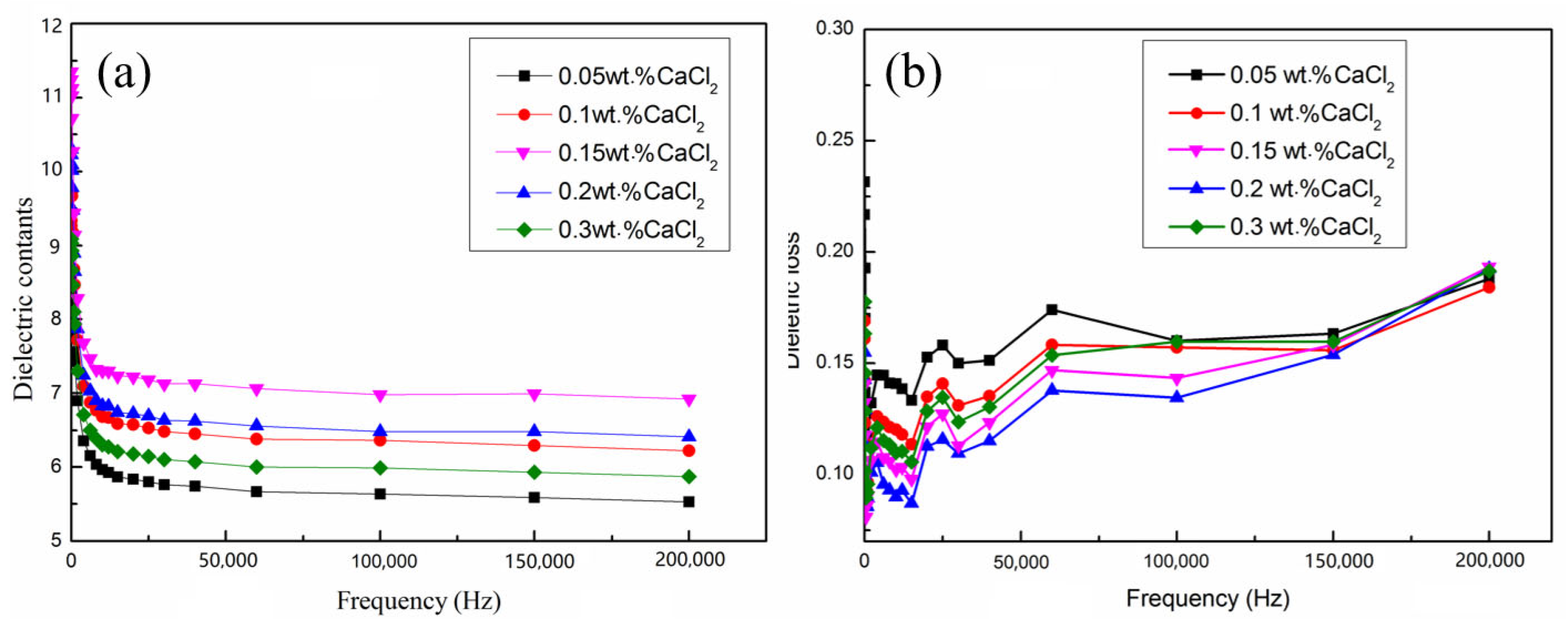
3.2. Electrical Properties of PVDF/CaCl2 Composite Films

Figure 7a is a graph of the dielectric constant of the PVDF/CaCl2 composite film with frequency. The dielectric constant of the PVDF composite film decreases with the increase of the frequency of the occurrence of dielectric relaxation. Due to the reduced mobility of the dipoles, the dielectric constant of the film decreases at high frequency, and as the frequency continues to rise, it tends to be stable. Additionally, it can be seen from the figure that when the CaCl2 content was 0.15 wt.%, the dielectric constant reached the maximum, its relative dielectric constant is about 11 at 1 kHz. The increase in the dielectric constant of the PVDF/CaCl2 composite film can be attributed to the addition of CaCl2, which increases the polar phase (β-phase) in the composite film. Because the β-phase content of the film with 0.15 wt.%CaCl2 reached the maximum, the relative dielectric constant of the composite film also increased greatly. In addition, due to the difference in electrical conductivity between the added CaCl2 and the PVDF matrix, this difference causes a large amount of the electric charge to accumulate on the interface under the action of the electric field, which causes the interface to be polarized, leading to an increase in the dielectric constant.
Figure 7b shows the relationship between dielectric loss and frequency change of the PVDF composite films. As the dielectric loss of the sample was measured at each frequency three times and its average value was taken, the value on the curve showed a slight fluctuation. However, from the general trend of change, the dielectric loss first decreases and then increases as the frequency increases. This is because the dipole polarization changes with the electric field at low frequencies, there is no delay loss and polarization loss, and the dipole of the film has enough time to orient under the AC electric field. However, when the frequency is at high frequency, the time for the dipole to move at high frequency is reduced, and the movement of the dipole cannot keep up with the change of the AC electric field. The continuous change of the orientation of the dipole causes a large amount of friction. Heat dissipation causes dielectric loss to rising at high frequencies. At this time, leakage loss is the main cause of loss. The leakage loss decreases with the increase of frequency, but the polarization loss increases with the increase of frequency and replaces the leakage loss as the main cause of the dielectric loss, which makes the dielectric loss of the PVDF film first decrease and then increase.

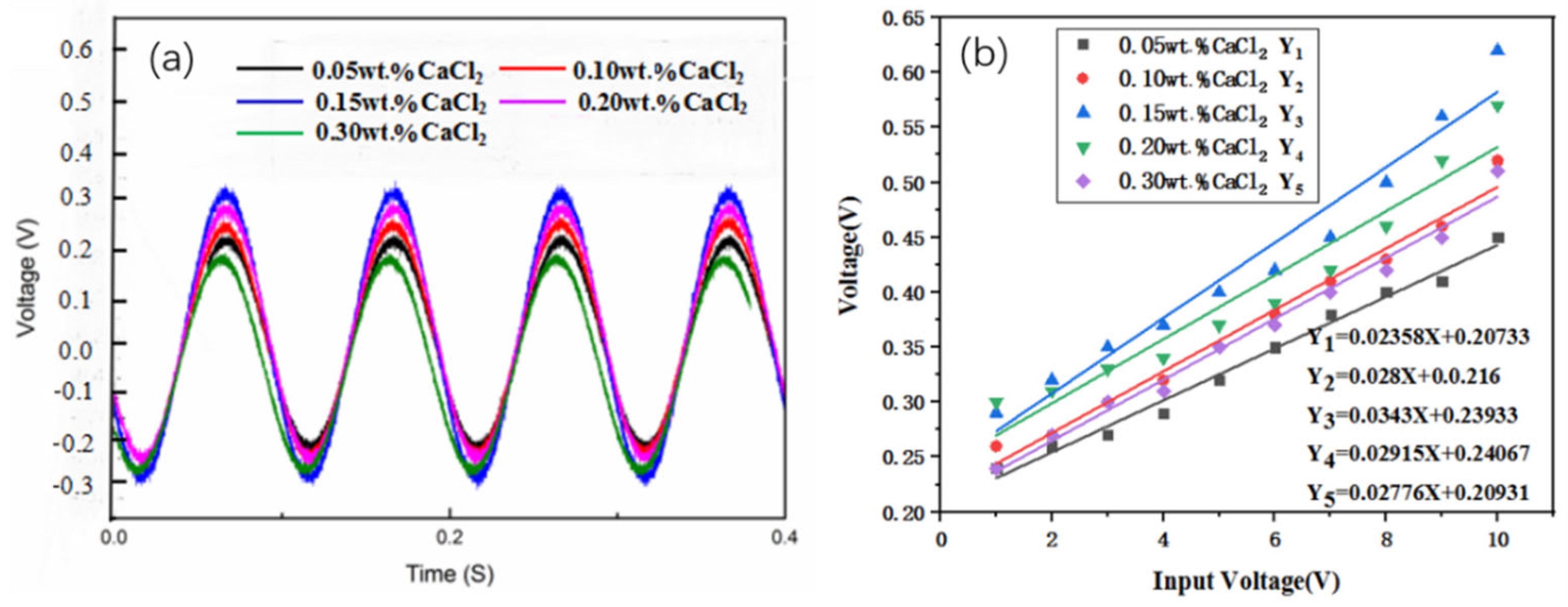
3.3. Performance of PVDF/CaCl2 Composite Film Sensor with Single-Layer Structure

Figure 8a is the output voltage of the single-layer PVDF/CaCl2 film sensor. The driving input voltage of the PZT is 10 V and the driving frequency is 10 Hz. The output voltage of the PVDF film sensor has the same frequency as the PZT drive voltage. When the CaCl2 content is 0.05 wt.%, the peak value of output voltage (VPP) is 0.43 V. While the CaCl2 content increases to 0.15 wt.%, the peak value reaches the maximum of 0.62 V. This is closely related to the higher β-phase content in PVDF/CaCl2 composite films. Furthermore, the output voltage of the single-layer PVDF/CaCl2 composite film sensor increases with the increase of the input voltage from 1 V to 10 V, the linear fitting result is shown in Figure 8b.
As we can be seen from Figure 8b, a good linear relationship is maintained between input and output voltages, the output voltage value of the PVDF composite film sensor changes with the change of the input voltage. With the increase of the driving voltage, the vibration amplitude of the manganese steel sheet will vibrate, and the deformation of the PVDF composite film sensor will change with the vibration of the manganese steel sheet. If the driving voltage is large, the deformation of the PVDF sensor is relatively large as well. The slope values (K) of the linear fitting of input and output voltages are shown in Table 2.
We know that different slopes of the linear fitting indicate different sensitivity of the PVDF film sensor. The greater the slope, the greater the sensitivity. It can be seen from Table 2 that the K value of PVDF composite film containing 0.15 wt.% CaCl2 is the largest, which means that its response to vibration is more intense and sensitive. This is essentially related to the amount of β-phase contained in the PVDF composite film. The more β-phase the composite film contains, the better the piezoelectric properties, thus the greater the response to the change of deformation, which leads to the higher sensitivity of the PVDF sensor.

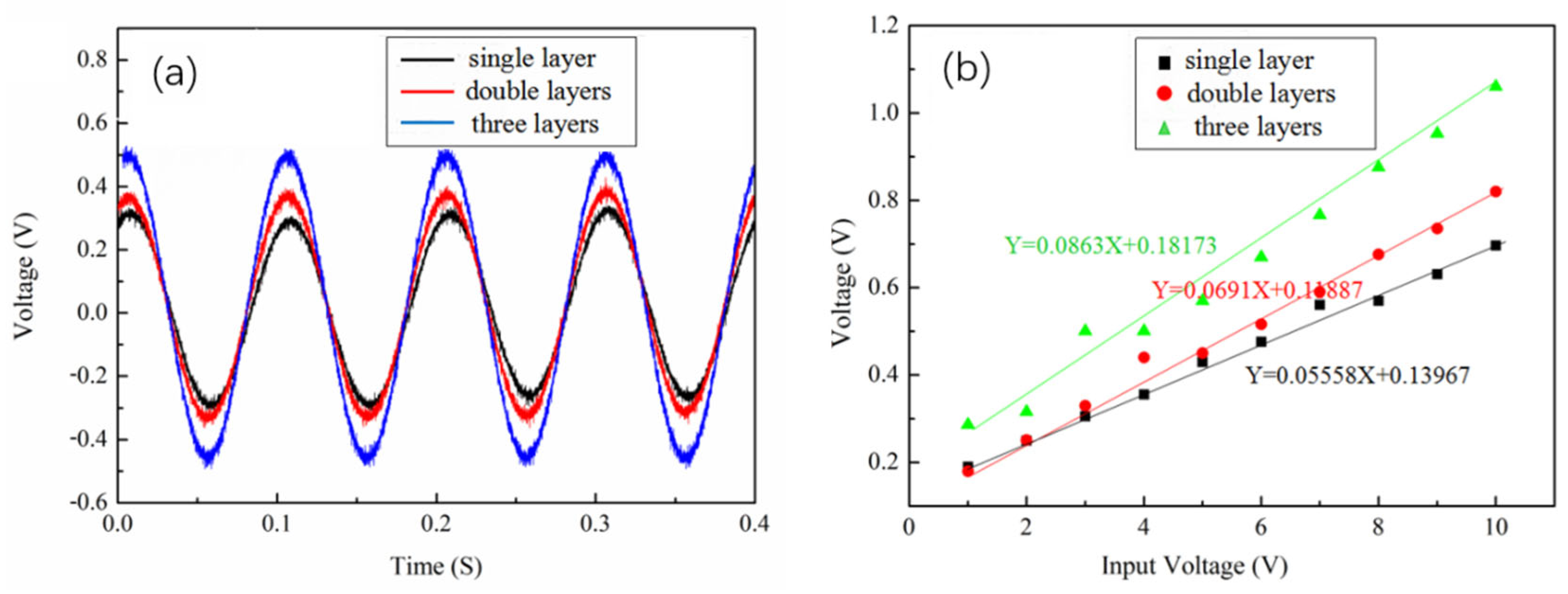
3.4. Performance Analysis of Multi-Layer PVDF/CaCl2 Composite Film Sensor

Figure 9 shows the relationship between the input and output voltage of a double-layer and three-layer PVDF/CaCl2 composite film sensor in series. From Figure 9a, the output voltage increases with the number of layers. When the sensor structure is in series and the number of layers is increased from one layer to two layers, the VPP value of the two-layer PVDF sensor increases from 0.62 V to 0.81 V at the input frequency of 10 Hz, 10 V voltage, 1.306 times that of the single-layer sensor. While the three layers reached 1.05 V, 1.296 times the two layers, and 1.693 times the single layer. The output signal and linear fitting equation of the driving voltage are shown in Figure 9b. The sensitivities of single-layer, double-layer, and three-layer sensors in series are 0.05558, 0.06910, and 0.08630, respectively. Obviously, the sensitivity of the three-layer PVDF/CaCl2 film sensor is higher than that of the double-layer sensor, and the double-layer sensor is higher than that of the single-layer sensor.
It is probably because the multi-layer PVDF/CaCl2 composite film sensor has multiple signal sensing devices in series. With the vibration of the cantilever beam, the performance of the sensor depends on the piezoelectric properties of each layer of PVDF/CaCl2 composite film. Moreover, multiple sensors have multiple deformation areas in series. The more the number of layers, the more deformation areas, and the deformation will generate more accumulated charge on the sensor surface. In addition, the capacitance values of the single-layer, double layer, and three-layer film sensors are 1008.900 pF, 500.467 pF, and 335.634 pF, respectively. Therefore, the sensitivity of the multi-layer sensor is improved.

4. Conclusions

In summary, the PVDF composite film with excellent electrical properties was prepared by adding 0.15wt.% CaCl2 using an electro-assisted 3D printing method. The addition of CaCl2 can reduce the pore size of the film, improve the quality of the film, and significantly increase the β-phase content and crystallinity of the PVDF films. The dielectric properties of PVDF/CaCl2 composite film also increase with the increase of β-phase content. Driven by external electrical excitation at 10 V and 10 Hz, the output voltage peak value of the PVDF/CaCl2 composite film sensor is 0.62 V, which is much higher than that of the pure PVDF film sensor. When the sensor structure is in series and the number of layers is increased from one layer to three layers, a good linear relationship is maintained between input and output voltage, the output voltage of PVDF composite film sensor with two and three layers is 1.306 and 1.693 times that of a single layer, respectively. The sensitivity of the multi-layer sensors has also been greatly improved.

Author Contributions

Writing—original draft, A.W.; resources, J.L.; data curation, C.S. and Y.Z.; supervision, C.C. All authors have read and agreed to the published version of the manuscript.

Funding

This research was supported by the National Natural Science Foundation of China, No. 52175464, the Jiangxi Provincial Natural Science Foundation, No. 20212BAB204047, and the Jiujiang Science and Technology Project, No. S2021ZDYFG089.

Institutional Review Board Statement

Not applicable.

Informed Consent Statement

Not applicable.

Data Availability Statement

All data included in this study are available upon request by the corresponding author.

Acknowledgments

This work was supported by Jiangsu Province Key Laboratory of High-end Structural Materials.

Conflicts of Interest

The authors declare no conflict of interest.

References

  1. Ribeiro, C.; Costa, C.M.; Correia, D.M.; Nunes-Pereira, J.; Oliveira, J.; Martins, P.; Gonçalves, R.; Cardoso, V.F.; Lanceros-Méndez, S. Electroactive poly(vinylidene fluoride)-based structures for advanced applications. Nat. Protoc. 2018, 13, 681–704. [Google Scholar] [CrossRef] [PubMed]
  2. Ramachandran, K.; Miscioscia, R.; De Filippo, G.; Pandolfi, G.; Di Luccio, T.; Kornfield, J.A. Tube Expansion Deformation Enables In Situ Synchrotron X-ray Scattering Measurements during Extensional Flow-Induced Crystallization of Poly l-Lactide Near the Glass Transition. Polymers 2018, 10, 288. [Google Scholar] [CrossRef] [PubMed] [Green Version]
  3. Wang, A.D.; Chen, C.F.; Zhu, Y.; Liao, L.C.; Qian, J.L.; Yuan, F.G.; Zhang, N.Y. Enhanced β-Phase in Direct Ink Writing PVDF Thin Films by Intercalation of Graphene. J. Inorg. Organomet. Polym. 2020, 30, 1497–1502. [Google Scholar] [CrossRef]
  4. Chen, C.; Cai, F.; Zhu, Y.; Liao, L.; Qian, J.; Yuan, F.-G.; Zhang, N. 3D printing of electroactive PVDF thin films with high β-phase content. Smart Mater. Struct. 2019, 28, 065017. [Google Scholar] [CrossRef]
  5. Chen, C.F.; Zhang, R.F.; Zhu, J.G.; Qian, X.Y.; Zhu, J.; Ye, X.; Zhang, M.Y. Direct writing polyvinylidene difluoride thin films by intercalation of nano-ZnO. Polym. Eng. Sci. 2021, 61, 1802–1809. [Google Scholar] [CrossRef]
  6. Sharafkhani, S.; Kokabi, M. Tailoring favor crystalline structure via electrospun PVDF/BaTiO3 nanofibers. In AIP Conference Proceedings; AIP Publishing LLC: College Park, MD, USA, 2018; Volume 1920, p. 020001. [Google Scholar] [CrossRef]
  7. Selvan, R.T.; Jayathilaka, W.A.D.M.; Chinappan, A.; Alam, H.; Ramakrishna, S. Modelling and Analysis of Elliptical Cantilever Device Using Flexure Method and Fabrication of Electrospun PVDF/BaTiO3 Nanocomposites. Nano 2020, 15, 2050007. [Google Scholar] [CrossRef]
  8. Karanth, P.N.; Desai, V.; Kulkarni, S.M. Modeling of single and multilayer polyvinylidene fluoride film for micro pump actuation. Microsyst. Technol. 2009, 16, 641–646. [Google Scholar] [CrossRef]
  9. Lee, H.Y.; Choi, B. A multilayer PVDF composite cantilever in the Helmholtz resonator for energy harvesting from sound pressure. Smart Mater. Struct. 2013, 22, 115025. [Google Scholar] [CrossRef]
  10. Zhao, J.; You, Z. A Shoe-Embedded Piezoelectric Energy Harvester for Wearable Sensors. Sensors 2014, 14, 12497–12510. [Google Scholar] [CrossRef]
  11. Spanu, A.; Pinna, L.; Viola, F.; Seminara, L.; Valle, M.; Bonfiglio, A.; Cosseddu, P. A high-sensitivity tactile sensor based on piezoelectric polymer PVDF coupled to an ultra-low voltage organic transistor. Org. Electron. 2016, 36, 57–60. [Google Scholar] [CrossRef]
  12. Musazzi, U.M.; Selmin, F.; Ortenzi, M.A.; Mohammed, G.K.; Franz’e, S.; Minghetti, P.; Cilurzo, F. Personalized orodispersible films by hot melt ram extrusion 3D printing. Int. J. Pharm. 2018, 551, 52. [Google Scholar] [CrossRef] [PubMed]
  13. Macedo, P.B.; Moynihan, C.T.; Bose, R. Glasses. Phys. Chem. 1972, 13, 171. [Google Scholar]
  14. Garain, S.; Sen, S.; Henkel, K.; Schmeißer, D.; Mandal, D. Enhancement of Electroactive β-phase and Superior Dielectric Properties in Cerium Based Poly(vinylidene fluoride) Composite Films. Mater. Today Proc. 2018, 5, 10084–10090. [Google Scholar] [CrossRef]
  15. Martins, P.; Lopes, A.C.; Lanceros-Mendez, S. Electroactive phases of poly(vinylidene fluoride): Determination, processing and applications. Prog. Polym. Sci. 2014, 39, 683–706. [Google Scholar] [CrossRef]
  16. Patro, T.U.; Mhalgi, M.V.; Khakhar, D.V.; Misra, A. Studies on poly(vinylidene fluoride)–clay nanocomposites: Effect of different clay modifiers. Polymer 2008, 49, 3486–3499. [Google Scholar] [CrossRef]
  17. Lewis, J.A. Direct Ink Writing of 3D Functional Materials. Adv. Funct. Mater. 2006, 16, 2193–2204. [Google Scholar] [CrossRef]
  18. Ramos, M.; Correia, H.M.; Lanceros-Mendez, S. Atomistic modelling of processes involved in poling of PVDF. Comput. Mater. Sci. 2005, 33, 230–236. [Google Scholar] [CrossRef] [Green Version]
  19. Ma, W.; Zhou, B.; Liu, T.; Zhang, J.; Wang, X. The supramolecular organization of PVDF lamellae formed in diphenyl ketone dilutions via thermally induced phase separation. Colloid Polym. Sci. 2012, 291, 981–992. [Google Scholar] [CrossRef]
  20. Peng, Y.; Wu, P.Y. A two dimensional infrared correlation spectroscopic study on the structure changes of PVDF during the melting process. Polymer 2004, 45, 5295–5299. [Google Scholar] [CrossRef]
  21. Montina, T.; Wormald, P.; Hazendonk, P. 13C Solid-State NMR of the Mobile Phase of Poly(vinylidene fluoride). Macromolecules 2012, 45, 6002–6007. [Google Scholar] [CrossRef]
  22. Ince-Gunduz, B.S.; Alpern, R.; Amare, D.; Crawford, J.; Dolan, B.; Jones, S.; Kobylarz, R.; Reveley, M.; Cebe, P. Impact of nanosilicates on poly(vinylidene fluoride) crystal polymorphism: Part Melt-crystallization at high supercooling. Polymer 2010, 51, 1485–1493. [Google Scholar] [CrossRef]
  23. Wang, A.D.; Chen, C.F.; Qian, J.L.; Yang, F.; Wang, L.; Zhang, M.Y. Enhanced Electrical Properties of PVDF Thin Film by Addition of NaCl by Near-Electric-Field 3D Printing. J. Electron. Mater. 2021, 50, 4781–4786. [Google Scholar] [CrossRef]
  24. Kuo, W.-K.; Shieh, M.-Y.; Yu, H.-H. Three-dimensional infrared absorption of hot-drawn and poled electro-optic PVDF films. Mater. Chem. Phys. 2011, 129, 130–133. [Google Scholar] [CrossRef]
  25. Liao, L.C.; Chen, C.F.; Qian, J.L.; Zhang, Y.M.; Zhang, R.F.; Zhu, J.G. Direct writing of PVDF piezoelectric film based on near electric field added by [Emim]BF4. Mater. Res. Express 2020, 7, 016437. [Google Scholar] [CrossRef]
  26. Wang, A.; Shao, M.; Yang, F.; Shao, C.; Chen, C. Preparation and properties of antibacterial PVDF composite thin films. Eur. Polym. J. 2021, 160, 110803. [Google Scholar] [CrossRef]
  27. Chen, C.; Zhu, J.; Zhang, Y.; Wang, A. Preparation and Luminescence Properties of PVDF/ZnS: Mn Flexible Thin-Film Sensors. Coatings 2022, 12, 449. [Google Scholar] [CrossRef]
Figure 1. (a) Schematic illustration and (b) preparation device for printing PVDF/CaCl2 composite film.
Coatings 12 00820 g001
Figure 2. Schematic diagram of a cantilever beam structure.
Coatings 12 00820 g002
Figure 3. SEM surface topography of (a) pure PVDF film and PVDF/CaCl2 composite films with (b) 0.05 wt.%, (c) 0.1 wt.%, (d) 0.15 wt.%, (e) 0.2 wt.%, and (f) 0.3 wt.% CaCl2.
Coatings 12 00820 g003
Figure 4. SEM transverse topography of (a) pure PVDF film and (b) PVDF composite film with 0.3 wt.% CaCl2.
Coatings 12 00820 g004
Figure 5. (a) XRD patterns and (b) FTIR spectra of PVDF/CaCl2 composite films.
Coatings 12 00820 g005
Figure 6. Mechanism of CaCl2 promoting PVDF transition from the α-phase to β-phase.
Coatings 12 00820 g006
Figure 7. Dielectric properties of PVDF/CaCl2 composite films (a) dielectric constant, (b) dielectric loss.
Coatings 12 00820 g007
Figure 8. (a) Output voltage of single-layer film sensor and (b) relationship between output and input voltages of single-layer film sensor.
Coatings 12 00820 g008
Figure 9. (a) Output voltage of multi-layer film sensors and (b) relationship between output and input voltages of multi-layer film sensors.
Coatings 12 00820 g009
Table 1. Crystallinity, F(β), and β phase content of PVDF/CaCl2 composite film.
Films with CaCl2Total
Crystallinity (%)
F(β)
(%)
β-phase
Content (%)
046.6778.1036.45
0.0555.7881.8445.65
0.1057.3182.1747.09
0.1558.6382.6748.47
0.2058.0382.5647.91
0.3056.1182.5346.30
Table 2. The slope values of the linear fitting of input and output voltages.
Films with CaCl20.05 wt.%0.1 wt.%0.15 wt.%0.20 wt.%0.30 wt.%
K0.023590.028000.034300.029150.02776
Publisher’s Note: MDPI stays neutral with regard to jurisdictional claims in published maps and institutional affiliations.

